Article

Design of a Linear Floating Active Resistor with Low Temperature Coefficient

School of Electrical and Electronic Engineering, Nanyang Technology University, Singapore 639798, Singapore
*
Author to whom correspondence should be addressed.
Chips 2025, 4(2), 18; https://doi.org/10.3390/chips4020018
Submission received: 9 March 2025 / Revised: 6 April 2025 / Accepted: 12 April 2025 / Published: 14 April 2025
(This article belongs to the Special Issue IC Design Techniques for Power/Energy-Constrained Applications)

Abstract

:
This paper presents the design and implementation of a linear, stable, low-power and PVT insensitive floating active resistor, which is realized using TSMC 40 nm CMOS process technology. By incorporating the automatic tuning circuit, this work has achieved improved performance metrics, which include low process sensitivity, reduced temperature coefficient, and good linearity. Monte Carlo (MC) simulations are conducted to evaluate the active resistor’s performance under variations in temperature, process, and supply voltage. The proposed design has demonstrated an average resistance process sensitivity of 0.64%, a temperature coefficient (T.C.) of 57 ppm/°C across −25 °C to 85 °C, and a linearity figure of merit (FOM) of 2.4 × 10⁻² V−1 with a resistance close to MΩ level. It can achieve a linear resistance tuning range of 430.5 kΩ to 1.714 MΩ. The typical power consumption of a single active resistor is 0.25 µW at 2.1 V bootstrapped supply voltage through a Dickson charge pump (DCP) circuit using a DC input of 1 V. These results have confirmed that the proposed active resistor can function as a robust and efficient resistor for low-voltage integrated circuits and systems.

1. Introduction

In analog CMOS integrated circuit design, high-accuracy components are required to ensure reliable performance across diverse applications. Resistors, as fundamental components, are critical in determining the precision of integrated circuits (ICs) for applications such as such as voltage and current reference circuits, analog filters, oscillators, programmable amplifiers and so forth. However, the use of traditional passive resistors in integrated circuits will display variations in both manufacturing tolerance as well as temperature sensitivity, thus limiting their applicability in precision designs [1,2,3,4,5]. Polysilicon resistors, often used in CMOS processes, have typical sheet resistance deviations of ±20%, making them unsuitable for high-accuracy applications without extensive trimming [1,6]. Moreover, the value of polysilicon resistors is fixed and not tunable [7]. Another critical limitation of passive resistors is the requirement for large chip area to achieve high resistance values, especially in ultra-low-power applications. This is particularly pronounced with a large scale of high-resistance resistors being employed in the design. As a result, such an increase leads to inefficient use of chip area and higher fabrication costs [3,8].
To address these issues, this paper addresses the design of a MOSFET-based active resistor in conjunction with the automatic tuning circuit. This brings the benefits of maintaining good linearity, reducing temperature sensitivity and suppressing wide process variation characteristics through the variation of the transistor’s parameters. As a result, the proposed active resistor can serve as a potential replacement for passive resistors in low-power voltage reference, current reference circuits and other analog circuit building blocks. This offers greater adaptability and improved stability in precision analog applications [6,9,10,11]. Furthermore, active resistors exhibit improved stability with respect to temperature and process variations and can be integrated using standard CMOS processes without the need for additional trimming circuits, which can reduce complexity and cost [8,12].
Regarding previous works, ref. [3] achieves ultra-low power and high resistance but it suffers from relatively lower linearity and larger T.C. due to mismatches in devices. This mismatch prevents the active resistor from fully replicating the resistance in the triode region because the triode transistors are sensitive to transistor parameters in variation. Meanwhile, ref. [6] offers relatively lower process sensitivity and a reduced T.C. but at the expense of increased circuit complexity. Its reliance on a differential difference amplifier (DDA) for control voltage generation introduces high circuit complexity and increased biasing current, resulting in greater power consumption. This raises the motivation for the investigation and the design of a floating active resistor with improved performance. Not only does it have low power consumption through the circuit simplicity in architecture, but it also provides low T.C. whilst offering good stability against PVT variation.
Section 1 presents the introduction. Section 2 presents the review of the representative active resistors. Section 3 details the proposed floating active resistor topology together with the automatic tuning circuit. Section 4 discusses the simulation results. Section 5 gives the conclusion.

2. Review of Representative Active Resistor

2.1. Parallel Compensated Active Resistor

A floating voltage-controlled resistor in CMOS technology with the method of nonlinearity cancellation is shown in Figure 1.
To achieve a floating voltage-controlled resistor, the work in [1] first analyzes the drain current characteristics of a MOS transistor operating in the triode region.
I D = μ C o x W L V G V B V F B 2 Φ F V D V S 1 2 V D V B 2 V S V B 2 + 2 3 μ C o x W L γ V D + V B 2 Φ F 3 2 + V S + V B 2 Φ F 3 2
where VG, VS, VD, VB are the gate, source, drain and substrate voltage with respect to ground, W and L are the gate width and length, μ is the effective mobility in the channel, Cox is oxide capacitance per unit area, VFB is the flat band voltage, ΦF is the substrate Fermi potential and γ is the body effect coefficient. If γ is considered to be small enough, the body effect can be neglected.
The primary nonlinearity comes from the quadratic term in the drain current equation. The cubic term in general is much smaller than the quadratic term. To tackle the non-linearity problem, a parallel compensated resistor [1] scheme is proposed. Two identical MOS devices with their channels connected in parallel and their gate voltages are biased by a respective dc voltage VC and coupled with ac voltages, VD and VS, through two source followers. Referring to [1], we have
V G A = V C + V D V G B = V C + V S
Assuming body effect is negligible and applying the substrate voltage VB, the two current expressions are given as follows:
I 1 A = μ C o x W L V C V T H V S D 1 2 V S D 2 + 2 3 μ C o x W L γ V D + V B 2 Φ F 3 2 + V S + V B 2 Φ F 3 2
I 1 B = μ C o x W L V C + V S D V T H V S D 1 2 V S D 2 + 2 3 μ C o x W L γ V D + V B 2 Φ F 3 2 + V S + V B 2 Φ F 3 2
The summed current ID is obtained as
I D = I 1 A + I 1 B = μ C o x W L 2 V C V T H V S D + 1 2 V S D 2 1 2 V S D 2 + 4 3 μ C o x W L γ V D + V B 2 Φ F 3 2 + V S + V B 2 Φ F 3 2 = 2 μ C o x W L V C V T H V S D + 4 3 μ C o x W L γ V D + V B 2 Φ F 3 2 + V S + V B 2 Φ F 3 2
where V T H represents the absolute threshold voltage of PMOS M1A and M1B. Through Taylor expansion of equation, the small-signal conductance between D and S becomes
R D S V C L 2 μ C o x W V C V T H
This arrangement effectively cancels the dominant even order nonlinearity and the odd order non-linearity is assumed to be small and ignored. As observed from Equation (6), the equivalent resistance is approximately linear. However, the second-order effects such as bulk modulation, mobility degradation and mismatch with transistor pair M1AM1B will degrade the non-linearity.

2.2. Floating Active Resistor with Common-Mode Generator Incorporating Bulk Effect

An alternative floating active resistor [2] is proposed and depicted in Figure 2. For a single triode transistor, the drain current expression is
I D = μ n C o x W L α 1 V D V S + α 2 V D V S 2 + α 3 V D V S 3
where
α 1 = V G V t h α 2 = 1 2 1 + γ 2 2 Φ F + V S B α 3 = γ 24 2 Φ F + V S B 3
with
V t h = V t h 0 γ 2 Φ F + γ 2 Φ F + V S B
where VD, VS, VG, VB represent the drain, source, gate and bulk potential, respectively. W and L are the gate width and length, μn is the effective mobility in the channel, Cox is oxide capacitance per unit area. ΦF is the substrate Fermi potential and γ is the body effect coefficient. VT0 is the threshold voltage at zero bias.
The main nonlinearity is caused by the quadratic term in the drain current equation, whilst the cubic term can be neglected due to the small value in general. To mitigate this, a specific gate voltage, taking into account the induced body effect within the common-mode voltage as the compensation term, is applied to the gate of the active resistor transistor M6. Hence, we have
V G 6 = V C + V t h 5 + 1 + γ 2 2 Φ F + V S B 5 V C M
where VCM is the common-mode voltage generated through M1M4 without any body effect. It is defined as
V C M = V D + V S 2
and VC is the dc bias voltage component generated using the level shifter. This is formed by M5 with a constant biasing current of 2I in conjunction with the common-mode generator. When M5 works in the saturation region and is subjected to bulk modulation though arranging VSB5 ≠ 0, the gate potential becomes
V G 5 = V D 5 = V G 6 = 2 2 I K 5 + V t h 5 + 1 + γ 2 2 Φ F + V S B 5 V C M
where
V t h 5 = V t h 0 + γ 2 Φ F + V C M + V S S 2 Φ F
The substrate voltage is fixed as −VSS and the source-bulk voltage of M5 is
V S B 5 = V C M + V S S
By substituting Equations (12)–(14) into Equation (7) and assuming that the cubic term is negligible, the drain current of the active resistor M6 is obtained as
I D 6 2 K 6 4 I K 5 V D S 6
Through the bulk induced common-mode voltage, the approach further eliminates the residual quadratic distortion term in the drain current, significantly improving linearity. The equivalent resistance of the active resistor M6 is approximated as
R 6 1 2 K 6 4 I K 5
The key achievement of this design is further reduction in nonlinearity arising from bulk modulation of Vth. As a result, the design ensures that the resistance value remains stable and independent of input voltage. This has illustrated its potential as an economic alternative with respect to other schemes used for applications requiring good linearity. Furthermore, the single active transistor eliminates the need of matching two transistors or more in the compensation process. Since it is relatively insensitive to mismatch effect, its technical merit is identified. Despite its strengths, the design also has certain limitations. The resistor’s performance will be degraded by mobility degradation that leads to odd order distortion. The circuit requires high supply voltage (±5 V) to sustain the operation. The common-mode generator also consumes significant power. This is not favorable when a large scale of active resistors is employed in low-power circuits and systems.

2.3. Grounded Active Resistor with Pre-Distortion Compensation

Another active resistor [3], which is aimed for use as a ground resistor, is depicted in Figure 3. The circuit consists of one main triode active transistor, MR, the replica triode transistors, M1 and M3, the saturation-based voltage mirror transistor pair M2 and M4, one operational amplifier (op-amp) and the pre-distortion block that comprises weak-inversion-based transistors M5M8 with identical size and an independent current source IB.
Through the clamping function of op-amp and identical matching design for M2 with M4, MR with M1 and M3, the relationship is established as follows:
V D R = V D 1 V D S R = V D S 1 I R = I D 3 = I D 1
As can be observed, I D 4 = I D 8 comes from the translinear loop [3] which is established among the transistors M5M6 with a relationship of
V G S 5 + V G S 7 = V G S 6 + V G S 8
This yields
I D 8 = I C = I R 2 I B
where IC is the compensated current coming from the pre-distortion block. This is forced to be equal to that of ID1 as drawn by the resistor network, which is formed by the nested configuration between the saturation transistor M2 and the triode transistor M1. Through the analysis of the network involving M1 and M2, we obtain
I D 1 = μ n C o x W L 1 V G S 1 V t h 1 V D S 1 1 2 V D S 1 2
I D 2 = 1 2 μ n C o x W L 2 V G S 2 V t h 1 2
and
V G S 2 = V D S 2 = V D 2 V S 2 = V G 1 V D 1 = V G S 1 V D S 1
Combining Equations (20)–(22), we have
I D 1 = 1 2 μ n C o x W L 1 1 1 + k 1 , 2 V G S 1 V t h 1 2
where k1,2 is defined as
k 1 , 2 = W / L 1 W / L 2
Similarly, we have the relation that
I D 3 = I D 4 = I R = I D 2 = I D 1 = I D 8
By substituting ID1 of Equation (23) into Equation (20), this gives
V D S 1 2 + 2 V t h 1 2 V G S 1 V D S 1 + 1 1 + k 1 , 2 V G S 1 V t h 1 2 = 0
Solving VDS1 in the quadratic Equation (26), we have
V D S 1 = 1 ± k 1 , 2 1 + k 1 , 2 V G S 1 V t h 1
The root term 1 + k 1 , 2 1 + k 1 , 2 V G S 1 V t h 1 is discarded because the condition for M1 to be biased in the triode region is based on the condition that V D S 1 < V G S 1 V t h 1 . Hence, the remaining root term for VDS1 is obtained as
V D S R = V D S 1 = 1 + k 1 , 2 k 1 , 2 I D 1 1 / 2 μ n C o x W 1 / L 1
and the effective resistance of the active resistor becomes
R A c t R R M 1 = V D S 1 I R = 1 + k 1 , 2 k 1 , 2 I D 1 1 / 2 μ n C o x W 1 / L 1 I R
By substituting IC from Equation (19) into Equation (29), we obtain
R A c t R 1 + k 1 , 2 k 1 , 2 1 1 / 2 μ n C o x W 1 / L 1 I B
As can be seen, through the independent design of separate bias current source IB, the stability of the resistor is translated to the stability of bias current source. The resistance of the active resistor becomes a stable, predictable value, unaffected by variations in the input current. Nevertheless, the key disadvantages of the resistor are not allowed to support floating resistor applications and the relatively high temperature coefficient (T.C.). This stems from the that fact that the performance of resistor topology relies on the matching among transistor group pairs such as triode transistors, sub-threshold transistors in the translinear loop. Different degrees of mobility degradation effect among the triode devices also contribute to the linearity issue.

3. Proposed Floating Active Resistor

3.1. Core Active Resistor Circuit

The proposed design distinguishes itself through its method of generating the common-mode voltage to ensure the effectiveness of the active resistor and the cancellation of second-order terms. Referring to Figure 4, the floating resistor consists of the common-mode generator formed by the transistors M3M4, a self-cascade composite transistor (SCCT) source follower formed by the transistors M7M8 and the current bias Ibias, and a native cascade transistor M0 comprising M1 and M2. The active resistor’s gate bias voltage is given as follows:
V G = V C + V C M V C M = m V D + V S 2
where VG is the tuned DC gate voltage applied to gate of the cascade transistor M0. VCM is the intermediate mid-point AC voltage obtained from the common mode generator. The parameter m [13,14] is given.
m = 1 + γ 2 2 Φ F + V S
The proposed design makes use of an NMOS native transistor as the active resistor, and hence, its bulk connection to the substrate will cause the body effect. Nevertheless, the body effect coefficient γ is usually small due to the lightly doped substrate. As a result, m 1 , and this yields
V C M V D + V S 2
Therefore, it is imperative to evaluate and compare the respective threshold voltage and respective body effect coefficient among the native transistor, LVT transistor and HVT transistor. The characterization involves grounding the bulk terminal and varying the source voltage VSB to observe the resulting change in threshold voltage Vth. Furthermore, the calculation of γ for a single transistor is given as
γ = V t h V S B V t h 0 V S B + 2 Φ F 2 Φ F
where Vth (VSB) represents the threshold voltage of the MOS transistor under a given source-bulk voltage VSB and Vth0 is the threshold voltage when VSB is zero and temperature is absolute zero. For native, LVT, and HVT NMOS transistors, Vth0 is equal to −158.4 mV, 340.1 mV and 397.2 mV, respectively. ΦF is the Fermi potential of the semiconductor, which is related to the doping concentration and temperature.
Figure 5a illustrates the variation of the threshold voltage Vth with respect to the source-bulk voltage VSB. As observed, the Vth of the native transistor changes the least as VSB varies when compared to other transistor types. Similarly, Figure 5b shows the relationship between the body-effect coefficient γ and VSB. At V S B = 0.3 V , the native transistor shows a γ value of approximately 23 m V , which is significantly smaller than the values of LVT and HVT transistors, at 186 m V and 207 m V , respectively. These results demonstrate that using native transistors effectively minimizes the impact of the body effect and facilitates the generation of a more precise and simplified common-mode voltage.
In addition, the long channel length L of the native transistor allows the realization of MΩ resistance level. With such a large L, the short-channel length effect can be effectively neglected. However, since the channel length cannot be infinitely increased due to physical and process limitations, a cascaded configuration of two native transistors is employed to further enhance the resistance value. This approach provides a practical and efficient method to achieve higher resistance without compromising performance significantly.
The voltage VCM is achieved by using diode-connected PMOS transistors in the cutoff region as the pseudo-resistors (PRs) with extremely large resistance, where the drain-source current is negligible [15,16]. As depicted in Figure 6, the PR group, which is arranged in symmetrical topology, is used to generate the common-mode voltage VCM instead of a single pair of pseudo-resistors.
When VSG > 0, each PR behaves as a diode-connected PMOS transistor. To ensure that the transistor operates in either the cutoff region or the subthreshold region, the condition VSG < |VTHP| must be satisfied. Under this condition, the transistor conducts only a few nA or even pA of current, resulting in an extremely high equivalent resistance for the PR. Consequently, the voltage drop across the PR remains negligible. When VSG < 0, the parasitic drain–n-well–source junction forms an unintentional pnp bipolar junction transistor (BJT), which can become activated. In this scenario, the PR behaves similarly to a diode-connected BJT [17,18]. However, since VD varies between 0 and 1 V while VS is fixed at 0.5 V, the maximum potential drop across a single PR is 0.25 V. This voltage is insufficient to forward-bias the parasitic diode, preventing significant conduction. As a result, the current remains extremely low, ensuring that the PR continues to function as a high-resistance element.
The small level drain-source current across each PR and the total leakage current Ileak are illustrated in Figure 7 with the change of the input signal, respectively. As observed, the leakage current is small enough to be negligible. Thus, the voltage drop across the transistors is nearly zero, leading to an intermediate voltage, which is almost half of the drain-source voltage.
The common-mode voltage VCM is plotted against the change of the input voltage VD from 0 to 1 V, as depicted in Figure 8. Since VS is fixed at 0.5 V, the value of VCM remains approximately equal to V D + V S 2 . The simulation results have validated a good common-mode generator using the symmetrical PR network.
VC is the DC voltage generated by level shifter formed by transistors M7M8 and Ibias, which is also called self-cascade composite transistor. SCCT structure is formed by M7 operating in the triode region and M8 operating in the saturation region, to enhance the performance of the source follower through addressing the key limitation on the short-channel effect [19,20]. The SCCT structure operates by utilizing M7 as a triode degeneration resistor to increase the bias voltage for the active resistor whilst increasing the output resistance of M8, which works in the saturation region. Thus, we have
V G = V C M + 2 I b i a s K M 8 + V t h 8 + I b i a s R D S 7
R D S 7 1 K M 7 V G S 7 V t h 7
V C = 2 I b i a s K M 8 + V t h 8 + I b i a s R D S 7
As can be seen in Equation (37), by adjusting the bias current Ibias, VC can be tuned to compensate the active resistor under PVT fluctuation. By applying the automatic tuning circuit, the current source Ibias will be replaced by the tuning current source Itune from the automatic tuning circuit, which will be discussed in the next section. The gate control bias voltage becomes
V C = 2 I t u n e K M 8 + V t h 8 + I t u n e R D S 7
Based on the triode transistor expression, we have
I D μ n C o x W L a 1 V D V S + a 2 V D V S 2 + a 3 V D V S 3
Due to the use of native transistor M1M2, VB is always equal to zero. This leads to V S B = V S . Thus, this gives
a 1 = V G V t h a 2 = 1 2 1 + γ 2 2 Φ F + V S a 3 = γ 24 2 Φ F + V S 3
V t h = V t h 0 + γ 2 Φ F + V S 2 Φ F
With the use of the native transistors M1M2 as the core active resistor, the characterization results have shown that the body-effect coefficient γ is approximately 23 m V . It indicates that γ is a very small value that can be neglected for approximation. Consequently, the control voltage is obtained as follows:
V G V C + V D + V S 2
Hence, the drain current becomes
I D μ n C o x W L V G V t h V D V S 1 2 V D V S 2
where the cubic term is ignored due to its small value. For the triode region, the terminal condition is given as
V G V t h > V D S
With V G V C + V D + V S 2 , the linearized resistance is obtained as
R e q L μ n C o x W V C V t h
It suggests that the resistance is dependent on the input voltage. Table 1 lists the sizes and types of components used in the proposed active resistor.

3.2. Proposed Automatic Tuning Circuit

The proposed active resistor topology incorporates a new automatic tuning circuit designed to dynamically stabilize resistance under variations in PVT [9,21,22,23]. As shown in Figure 9, the topology combines a dual operational amplifier configuration with each consuming 500 nA supply current, a reference voltage Vref, current sources formed by M9, M10, and M11 and two compensation MOS capacitors [24] C1 and C2 used to stabilize the two amplifiers.
These two capacitors not only provide a frequency compensation function, but they also suppress the high-frequency transients in the feedback loops since the disturbances come from the supply line. As a result, they stabilize overall circuit performance in the presence of ripple at the supply line. These capacitors with parallel configuration are shown in Figure 10. The unit capacitor for the compensation capacitor is 25 pF and N is the multiplier of the active capacitor.
The automatic tuning circuit is responsible for generating the tuning current Itune, which dynamically adjusts the resistance of the active resistor against environmental, process-induced variations [21,22,23,25]. On top of that, two passive resistors with opposite T.C. are connected in series to achieve close to zero T.C. for the combined resistor R. The negative feedback mechanism ensures that the voltage across R is close to Vref, through dynamically adjusting the output of the amplifier to produce Itune1 according to the following relationship:
I t u n e 1 = V r e f R = I r e f
This current is scaled down by the current source transistor M10, with respect to M9 by M times.
I t u n e 2 = 1 M I t u n e 1
where M is the multiplier. Since both transistors M9 and M10 operate in the saturation region whilst employing long channel design, it permits Itune2 to track well with the scaled Iref. Due to the usual large resistance of MΩ level realized by the active resistor (ActR), the Itune2 is made sufficiently small to avoid excessive voltage drops across ActR.
The loop2 in the automatic tuning circuit plays a pivotal role in generating Itune to provide adaptive current to bias and tune the active resistor against PVT variation. As a result, it provides a separate control whilst correlating with respect to Itune1 and Itune2. When the reference current Itune2 flows into the ActR, a feedback voltage is established at V and is compared with Vref. The negative feedback adjusts its output to ensure that the tuning current Itune is dynamically regulated by M11, which works in the subthreshold region. This current serves as a replacement for the intrinsic bias current Ibias within ActR, as shown in Figure 4. Through this action, variation of process parameters, such as transconductance and threshold voltage, etc., in the active resistor, are compensated such that the active resistance of ActR is tracked with the constant value of passive resistor R.
Moreover, Itune1 (generated by M9) and Itune (generated by M11) belong to different feedback loops, and their associated resistances are also different levels. M9 and M10 operate in the saturation region to provide stable mirror currents with respect to the reference current Iref. On the other hand, M11 operates in the sub-threshold region. It offers high transconductance gm, which aims to increase the feedback loop gain for loop control at low current level design in the context of minimizing the power consumption. As shown in Figure 9, the current source transistor M17 further copies the current Itune from the transistor M11. This is used to bias the ActR. This configuration enables the realization of a fully floating active resistor. Table 2 lists the size of components in the automatic tuning circuit.
As illustrated in Figure 11, the op-amp consists of three main parts: the start-up circuit, the bias circuit, and the core circuit. Each sub-circuit plays a critical role in ensuring the proper functioning of the op-amp, which is used in the automatic tuning circuit to clamp the two input voltages (V+ and V) to the same level, a necessary condition for maintaining stable and precise operation.
The start-up circuit, comprising MP6 and MP7, and the capacitor CS, is designed to ensure that the bias circuit initializes correctly during power-up. In many self-biasing circuits, there is a risk of the system entering a metastable state where the current through the circuit is zero, preventing the bias circuit from functioning. This is called the degenerating point. The start-up circuit injects an initial current to avoid this uncertainty and to get rid of the degenerating point. The capacitor CS ensures that the start-up mechanism is transient, allowing the bias circuit to take over in steady-state operation once the system stabilizes itself. As such, the start-up circuit does not add extra power consumption.
The bias circuit consists of transistors MP3, MP4, MN5, MN6, and the resistor R3. This loop generates the bias current Ibias for the op-amp. The transistors MN5 and MN6, along with R3, form a self-regulating feedback loop. The resistor R3 sets the reference voltage that determines the bias current. The feedback ensures the voltage at the gate of MP4 in stabilized condition, thereby setting a stable Ibias that is mirrored to the other part of the circuit. As a result, the op-amp operates in its active region, providing the required clamping functionality for V+ and V.
Referring to the op-amp core circuit, it consists of MP1, MP2, MP5, MN1, MN2, MN3, MN4, serving as one of the parts in the automatic tuning circuit. The op-amp’s primary role in the automatic tuning circuit is to clamp V+ and V to the same level. This is achieved through its open-loop gain of 47.1 dB, which ensures a small difference between V+ and V in application. This adjustment allows the op-amp to effectively maintain the stability and precision of the automatic tuning circuit. Additionally, the op-amp exhibits a PSRR of 94.3 dB, ensuring that variation in the supply voltage minimally affects its circuit performance. Furthermore, its CMRR of 62.4 dB enhances its ability to reject common-mode noise or disturbances in the input signal. The op-amp in the automatic tuning circuit has a bandwidth of 4.1 kHz, which is considered sufficient for low-frequency tuning and control applications. The simulation results are shown in Figure 12. Table 3 illustrates the size of components in op-amp.

3.3. Dickson Charge Pump (DCP)

The proposed design needs a higher voltage supply required for the automatic tuning circuit to ensure that the native resistor is biased in the triode region and higher voltage supply for the op-amp, but the DC 1 V supply is insufficient. To address this issue, the voltage conversion circuit is essential to boost the supply voltage to meet operational requirements. Among the various DC-DC conversion techniques, DCP is widely used in such applications due to their compactness, ability to generate multiple voltage levels, and absence of bulky components, making them highly suitable for integration in modern CMOS circuits [26,27]. Moreover, by employing the charge pump, the design achieves insensitivity to the variation in the original VDD supply voltage, ensuring stable performance across different supply conditions. To account for the variations caused by different process corners and temperature-induced degradation, the voltage level boosted by the charge pump can reach a maximum of 2.2 V. The exemplary output voltage of the charge pump is illustrated in Figure 13.
The operation of DCP can be described as a sequential process involving three key phases: charging, boosting, and voltage multiplication, as shown in Figure 14.
During the charging phase, when the first clock signal CLK1 is active, the charge is transferred from one capacitor Ci to the next through the forward-biased MOS diodes, enabling the storage of charge along the capacitor chain. In the boosting phase, when the second clock signal CLK2 (the inverted counterpart of CLK1) is active, the boosted potential generated at the preceding stage is utilized to transfer additional charge to the subsequent stage, thereby incrementally increasing the voltage level [28]. This process is repeated across multiple stages of the charge pump, resulting in a progressive voltage multiplication. The output voltage at the final stage is approximately equal to the input voltage VDD plus the cumulative contributions from each stage, which are determined by the amplitude of the clock signal minus any voltage drops due to parasitic resistances and threshold voltages of the MOS diodes [29]. This stepwise transfer and boosting process makes use of the capacitor voltage dynamics.
Q = C Δ V
where Q represents the amount of electric charge stored on the capacitor plates and ΔV is the voltage difference across the capacitor’s plates. ΔV across a capacitor cannot change instantaneously due to the fixed Q in each step. This ensures stable and predictable voltage increments at each stage.
In the context of the proposed design, the ring oscillator serves as the clock generation unit, producing the biphasic signals CLK1 and CLK2 with a short non-overlapping period, as shown in Figure 15. This is achieved by incorporating a non-overlapping clock generation circuit. The frequency of the clock is 3.08 MHz. The non-overlapping clock generator ensures that two complementary clocks CLK1 and CLK2 do not overlap during their transitions. Overlapping between these clocks could result in short-circuit currents within the switches of the charge pump, reducing its efficiency and increasing power dissipation. The non-overlap period is introduced using a delay chain, typically implemented with cascaded inverters and NAND gates. Thus, the non-overlapping design is critical for ensuring the performance of switched-capacitor circuits [30].
However, it is important to note that the charge pump introduces inherent ripple into the boosted power supply, which can affect the performance of the circuit if the ripple is not well suppressed. To mitigate this issue, an integrated second-order RC low-pass filter comprising R5C6 and R6C7 is implemented, as shown in Figure 16.
This filtering effectively reduces the ripple voltage down to 2.54 mV, corresponding to a ripple coefficient of 0.18%, which is negligibly small enough to cause an impact on the circuit’s performance. The proposed DCP is designed to provide a voltage from a DC 1 V to a typical bootstrapped value of 2.1 V, providing power to the entire circuit. Under all process corners, the charge pump achieves a maximum output voltage of 2.2 V, delivering a maximum load current of 9.5 µA. This translates to drive an effective load of 231 kΩ. Table 4 shows the component types, sizes and their values in the DCP design.
The resistance of the active resistor after integrating the DCP into the circuit is shown in Figure 17. As observed, the resistance of the active resistor with the charge pump introduced exhibits very minute fluctuations across the TT, SS, FF, SF, and FS process corners, with variations of approximately 2.2 kΩ, 3.7 kΩ, 2.1 kΩ, 2.7 kΩ, and 2.5 kΩ, respectively. To assess the impact of the fluctuation, their magnitudes were normalized based on the corresponding steady-state resistance value, resulting in variations of 0.24%, 0.35%, 0.29%, 0.30%, and 0.28%, respectively. The observed fluctuation is negligibly small. This indicates that the ripple-induced resistance variation in this design is insignificant and does not pose a concern for circuit performance.

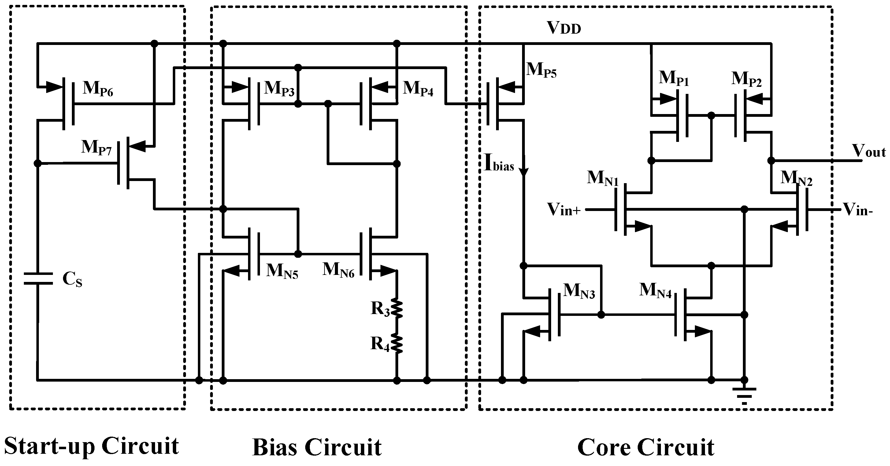
4. Results and Discussions

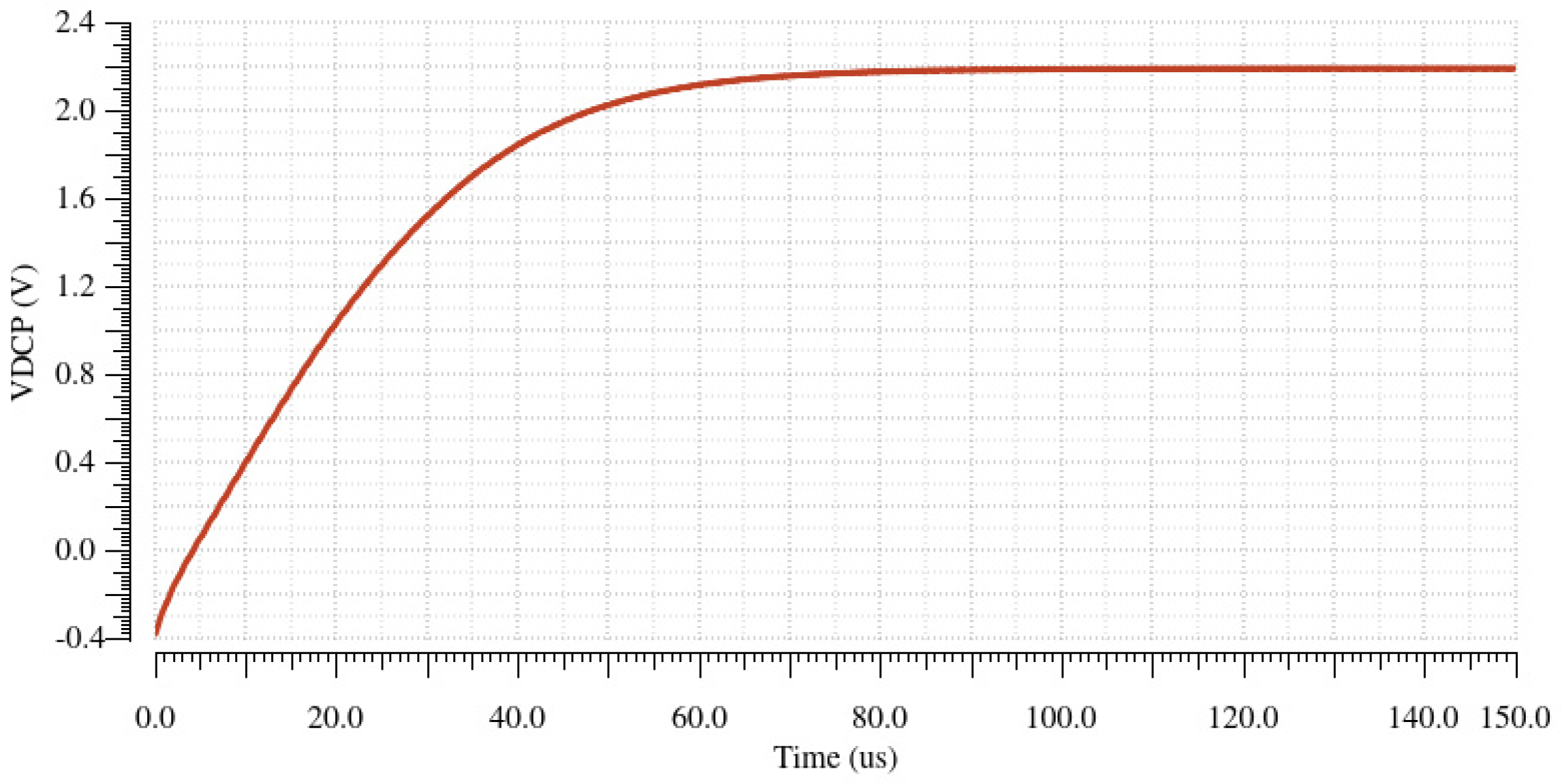
The proposed active resistor, realized using TSMC 40nm CMOS technology, operates at a typical bootstrapped supply voltage of 2.1 V from the DC 1 V input voltage. To compare the variation of resistance with the input voltage, the linearity figure of merit (FOM) is defined as follows:
L i n e a r i t y o f F O M = 1 R n o r R max R min V o l t a g e R a n g e
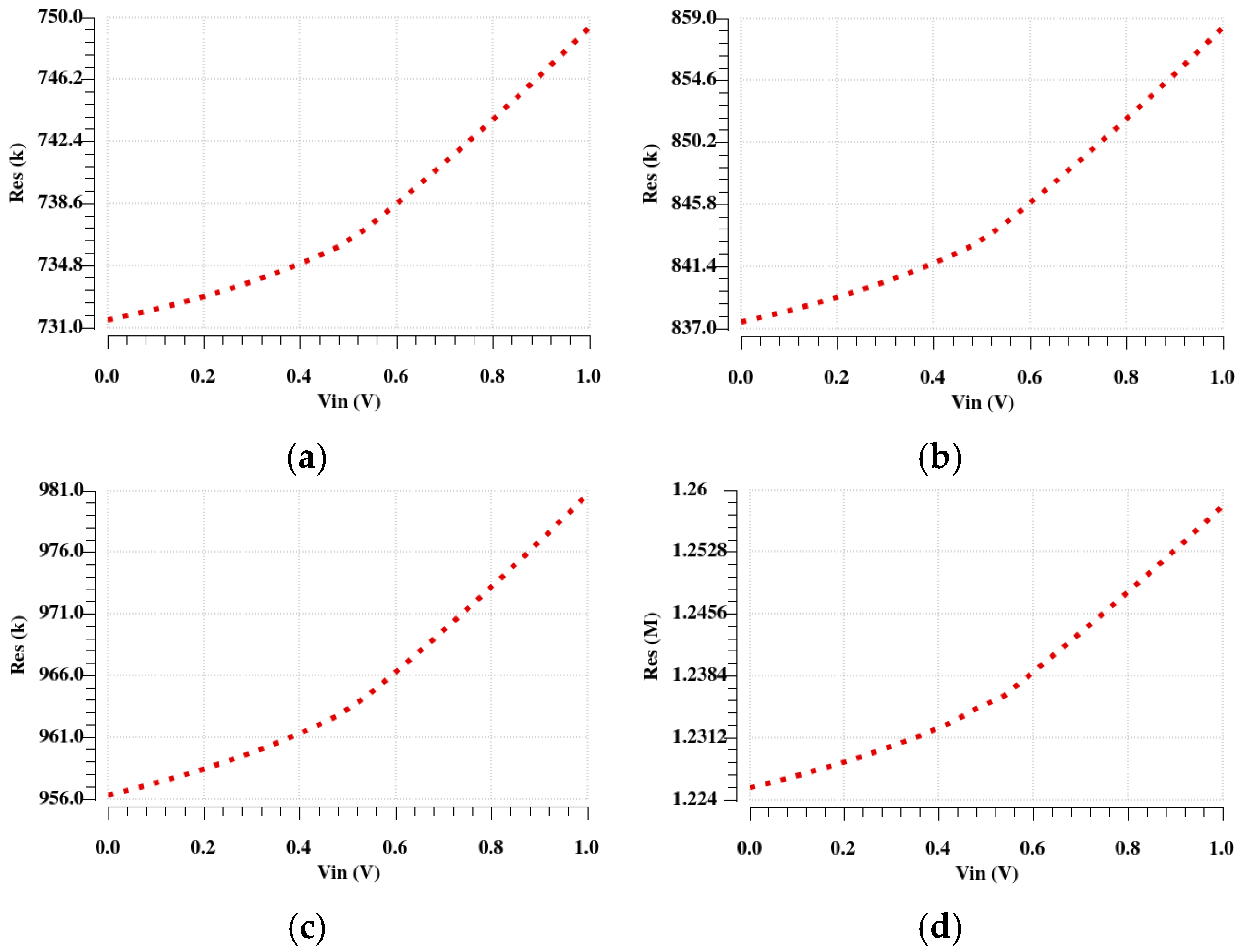
It can be seen that the resistance variation is evaluated at different temperatures, such as −25 °C, 0 °C, 27 °C, and 85 °C. Then, the linearity of the resistance can be assessed.
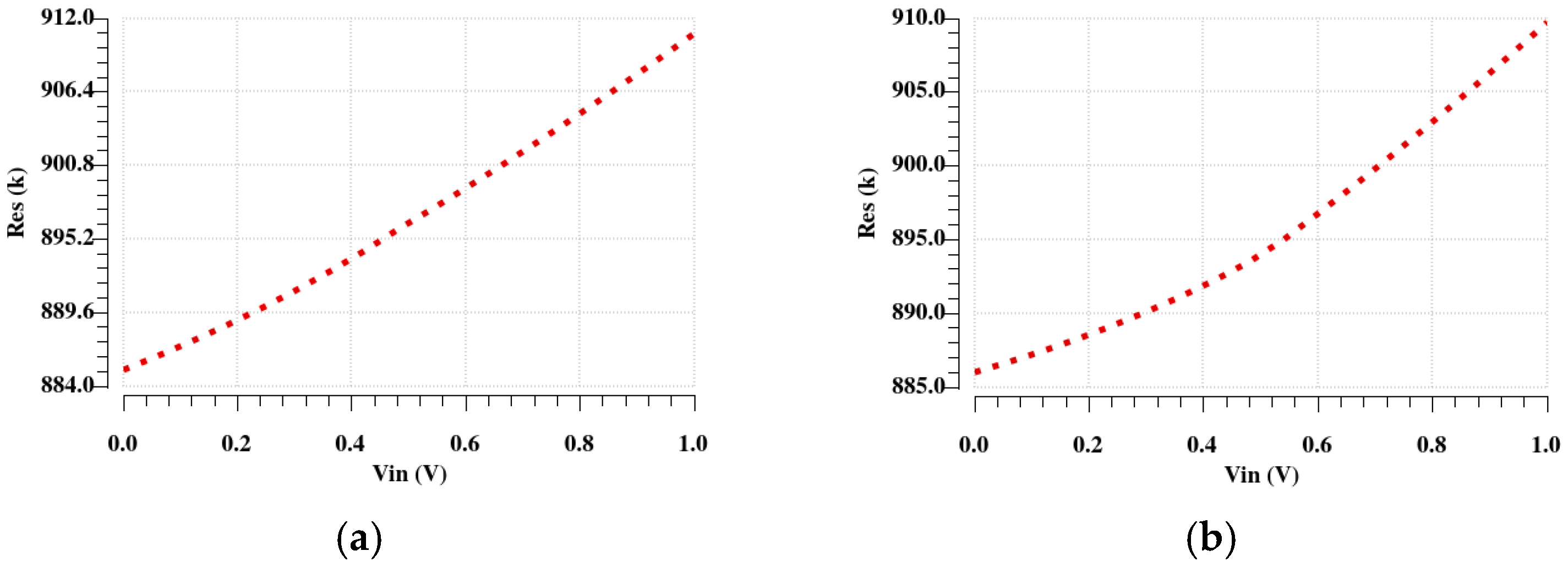
 Figure 18 and Figure 19 show the results before and after applying the automatic tuning, respectively. The term R max R min V o l t a g e R a n g e represents the resistance change with respect to the range of applied voltage. The smaller the value, the better the stability of the resistance. Dividing by Rnor ensures that the linearity measure is independent of the absolute value of resistance through normalization. This makes it suitable for comparing resistors at different nominal values.
In order to compare the linearity FOM numerical value with and without automatic tuning circuit, the calculated results at different temperatures are summarized in Table 5.
The results have revealed that without the tuning circuit, the linearity FOM remains relatively stable across temperatures, ranging from 1.7 × 10 2   V 1 to 2.6 × 10 2   V 1 , suggesting that the resistance variation with input voltage is within a reasonable range. With the tuning circuit, the variation of linearity FOM suggests that the resistance is dependent on the input voltage across most temperature conditions, but leads to some increase in nonlinearity at extreme temperatures of −25 °C and 85 °C, at 2.8 × 10 2   V 1 and 3.1 × 10 2   V 1 , respectively. Nevertheless, the increase is within an acceptable range.
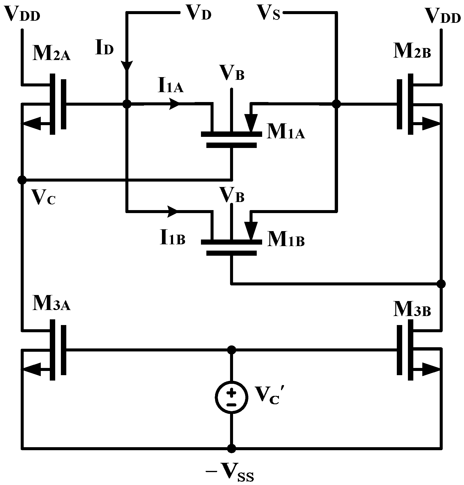
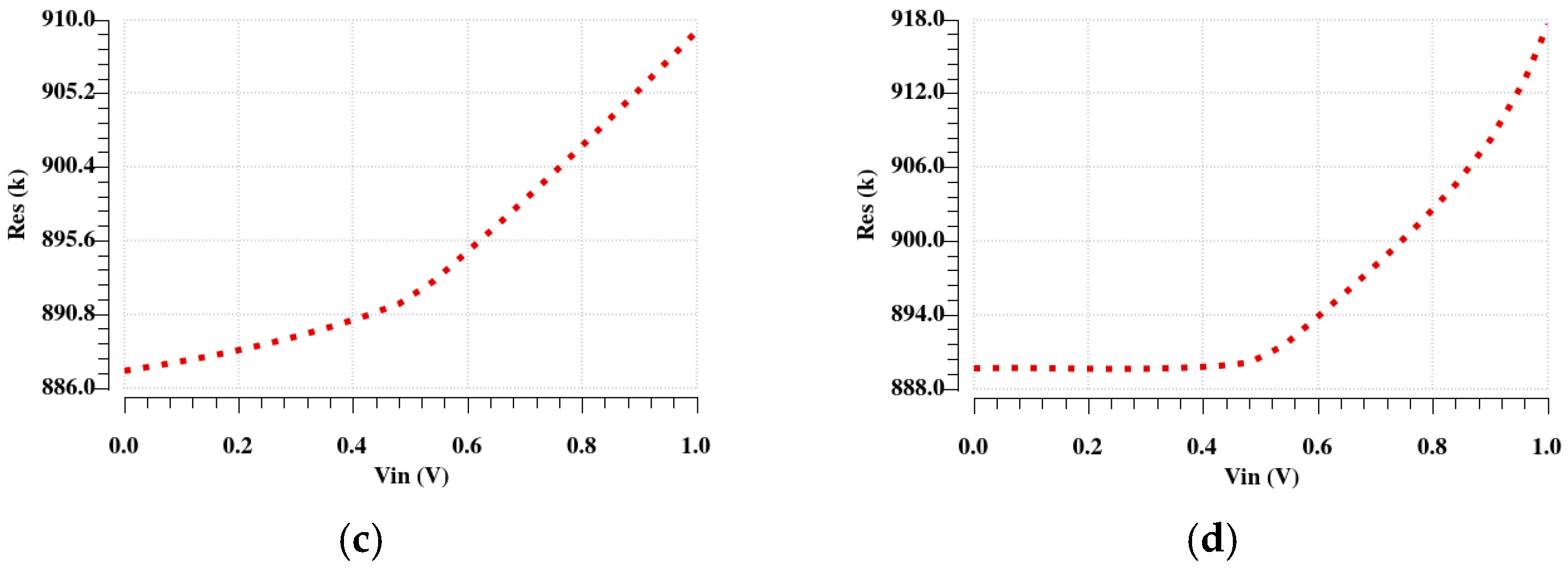
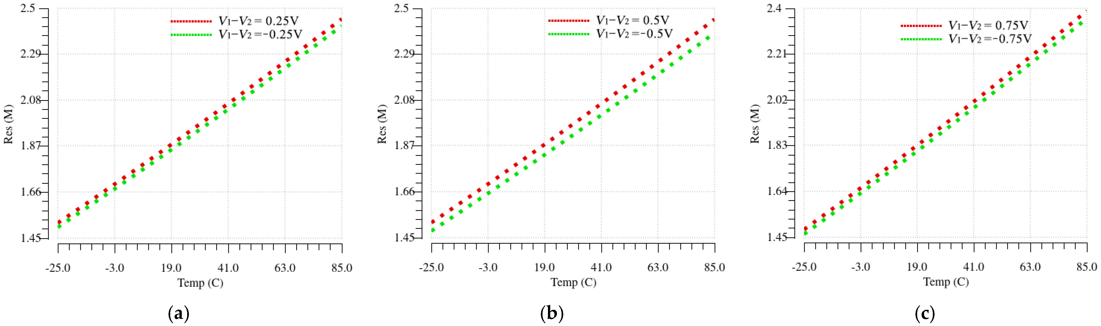
Furthermore, the resistance variation with temperature needs to be evaluated. This is achieved by controlling different drain-source voltages (V1V2), such as ±0.25 V, ±0.5 V, and ±0.75 V, while the resistance change over temperature is recorded. This setup also serves to demonstrate that the floating resistor can accommodate bidirectional signal flow, ensuring stable operation across varying input conditions. The ability to maintain consistent resistance characteristics in both positive and negative voltage scenarios further highlights its adaptability in practical applications. Figure 20 and Figure 21 illustrate the resistance variation without and with the automatic tuning circuit.
In order to compare the TC performance without and with the automatic tuning circuit, the calculated values are summarized in Table 6.
Table 6 presents a comparison of T.C. before and after applying the automatic tuning circuit. Without the tuning circuit, the T.C. remains consistently high at about 4.3 × 10³ ppm/°C. This has confirmed significant high temperature sensitivity. However, with the tuning circuit, the T.C. is dramatically reduced to the worst maximum value of 61.36 ppm/°C, demonstrating an improvement by nearly two orders of magnitude. This significant reduction in T.C. highlights the effectiveness of the automatic tuning circuit in compensating for the variation of transistors’ parameters in the active resistor against temperature change. This permits the active resistor to maintain a stable resistance across different operating conditions.
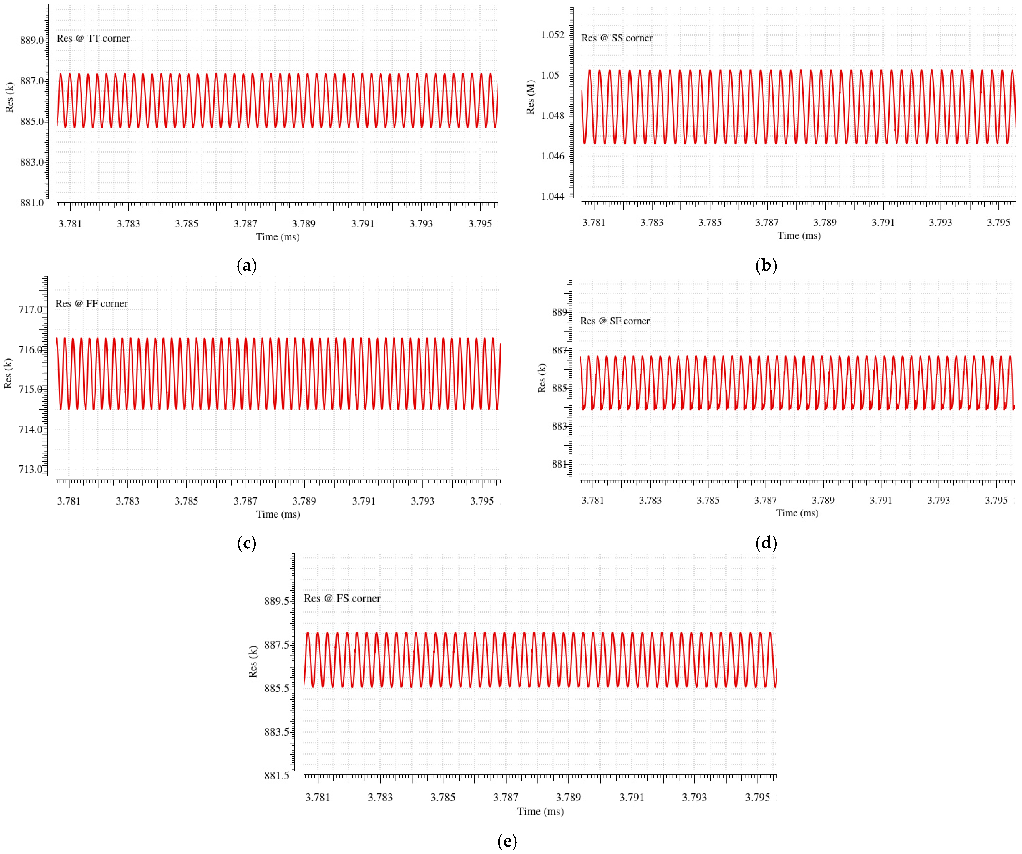
The Monte Carlo (MC) simulation results of the proposed active resistor will reveal a statistical analysis of its resistance change against the temperature variation at different process corners. Figure 22 shows the MC simulation of the resistance, which is conducted over 800 samples, under TT, SS, FF, SF, and FS process corners at a bootstrapped supply voltage of 2.1 V.
The corresponding statistical data are summarized in Table 7. With the automatic tuning circuit, the average resistance values for the TT, SS, FF, SF, and FS process corners are obtained as 887.41 kΩ, 1.05 MΩ, 716.19 kΩ, 886.63 kΩ, and 888.20 kΩ, respectively. These results have indicated a stable performance, with the resistance variation being well contained within acceptable ranges. The SS corner represents the extreme process conditions with the largest deviation from the nominal resistance. The SS corner corresponds to slower transistors with higher resistances, while the FF corner corresponds to faster transistors with lower resistances. The SF and FS corners with respect to the TT corner display a similar level of process sensitivity.
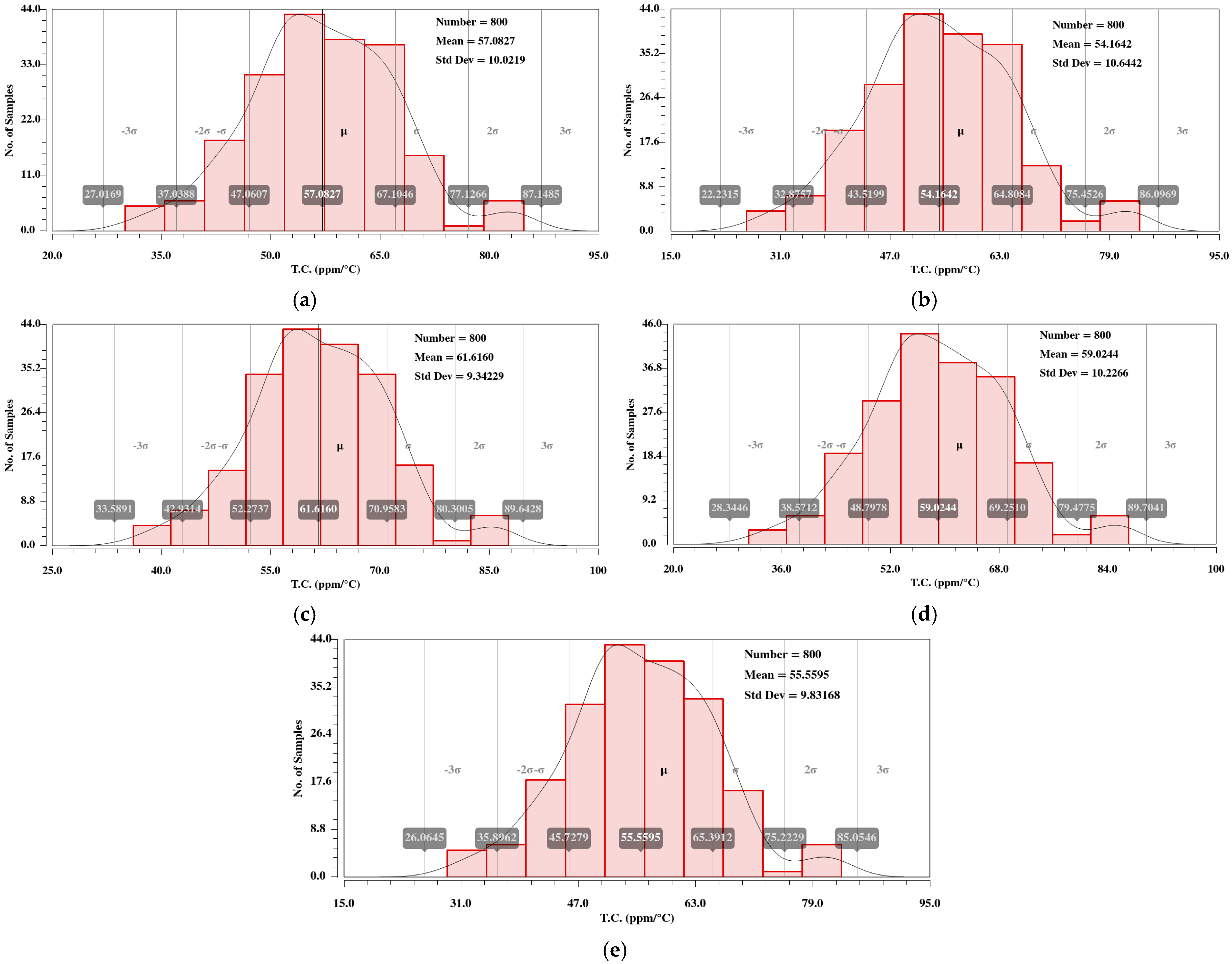
For the analysis of the active resistor’s T.C. with temperature range from −25 °C to 85 °C in statistical performance, the MC simulation results are shown in Figure 23.
The statistical data values pertaining to the sensitivity of the active resistor at different process corners are summarized in Table 8.
The T.C. values for the TT, SS, FF, SF, and FS corners, under automatic tuning circuit, are obtained as 57.08 ppm/°C, 54.16 ppm/°C, 61.61 ppm/°C, 59.02 ppm/°C, and 55.56 ppm/°C, respectively. These results have demonstrated that the active resistor exhibits a reasonably low T.C. across most corners, except for the FF corner, where the value increases to a certain extent due to faster transistors but still an acceptable value. The calculated sensitivities for TT, SS, FF, SF, and FS corners are 17.55%, 19.64%, 15.15%, 17.32%, and 17.69%, respectively. The low sensitivity reflects the effectiveness of the compensation strategies employed, ensuring robust operation over a wide temperature range. However, the increased T.C. and sensitivity in the SS corner suggest that the process variation can increase the resistor’s temperature dependency to an acceptable extent.
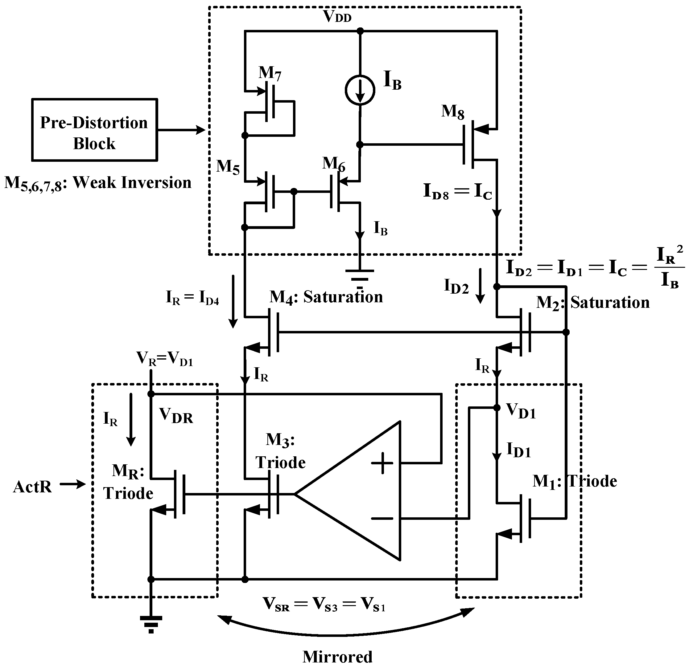
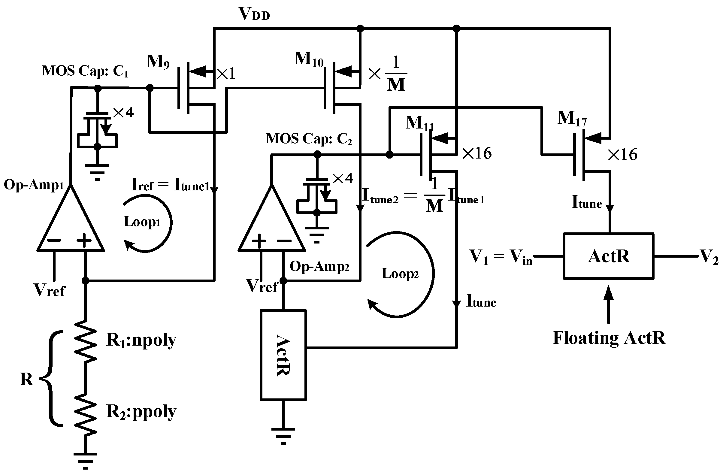
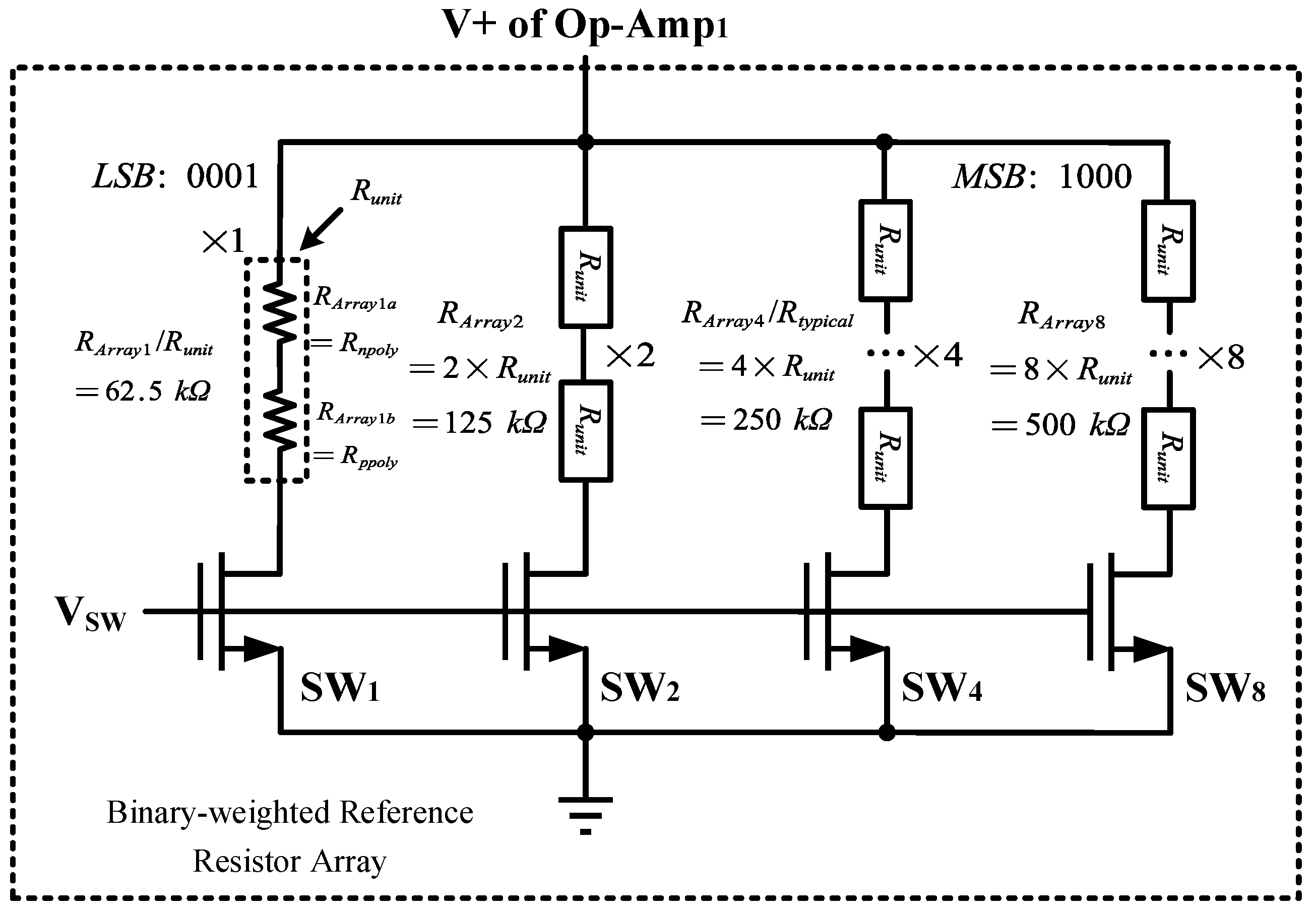
Moreover, the resistance of the active resistor should be tuned for practical applications. A tuning strategy is implemented by the binary-weighted reference resistor array. Specifically, the reference resistor in Figure 9 is replaced by four reference resistors with binary weights (1, 2, 4, and 8) [31] which are configured in a switchable array, enabling adjustment of the tuning current by digital means, as shown in Figure 24. The typical resistor used in the automatic tuning circuit is split into four unit resistors. Each unit resistor comprises two passive resistors with opposite T.C. They are series-connected to achieve close to zero T.C. for the combined resistor Runit. Table 9 shows the device types and sizes for the binary-weighted reference resistor array.
As a result, the resistance tuning range is significantly expanded, achieving values from approximately 430.5 kΩ to 1.71 MΩ. This corresponds to a tuning range greater than ±50% around the nominal value, which is denoted as 887.4 kΩ in this design. The resistance of ActR in response to the change of frequency is shown in Figure 25. It can be observed that the ActR resistance remains constant when frequency is up to about 4.6 kHz before dropping in value. This design provides enhanced flexibility and control over the resistor’s value, thus making it suitable for various application requirements.
The performance comparison demonstrates that the proposed active resistor design achieves technical merits such as process sensitivity, temperature stability, wide tuning range of the resistance, very low power consumption and good linearity. The performance results of active resistors are compared with those of the representative reported works in Table 10.
Since many ActRs can share the same control unit, the overhead design for the proposed work is significantly reduced when compared to others [3,6,33] in which each active resister relies on an individual control unit. Referring to Table 10, the proposed design achieves a process sensitivity of 0.64% corresponding to the resistance variation, which is lower than that of prior works with sensitivity of 1.33% [9]. With the automatic tuning circuit, the temperature coefficient (T.C.) is reduced to 57 ppm/°C over a wide temperature range of −25 °C to 85 °C with the sensitivity of 17.55%. The T.C. with the tuning circuit is 80 times lower than that without the tuning circuit. It is a significant improvement compared to T.C. of up to 500 ppm/°C in earlier designs [6]. These results have shown the robustness of the proposed design against process and temperature variation through the effective use of automatic tuning and temperature compensation techniques.
In terms of linearity, the reported design has achieved a good result of 2.4 × 10⁻² V−1. Regarding power consumption, the single active resistor only dissipates 0.25 µW under a low bias control current of 121 nA. Additionally, the total power consumption of the active resistor with the automatic tuning circuit is approximately 13 µW. When the charge pump is included, the overall power consumption is 42 µW. These indicate that it is suitable for realization in low-power and compact systems.
As interpreted from Table 10, it can be observed that after applying the tuning circuit, the temperature and process sensitivity increase in value, though not by much. This is primarily because the tuning circuit forces ActR to track the temperature behavior of the passive resistor R, whose resistance value can vary differently across process corners and temperature variation. Another reason is that of the variation of the tuning circuit’s loop gain under different process corners. To verify the issues, the T.C. of the passive resistor R and the loop gain pertaining to loop2 variation across five standard process corners are evaluated and shown in Table 11.
The slight change in the T.C. of the passive resistor across process corners and the moderate loop gain fluctuation in the tuning circuit contribute the imperfections in this circuit implementation. However, as can be observed from the good stability in overall performance, their influences are considered insignificant.
In summary, the proposed active resistor has demonstrated an excellent balance among power, linearity and T.C., while addressing key limitations of earlier reported designs and offering an economical design perspective in which many PRs can share one common control unit.
To demonstrate the practical application of the proposed active resistor, a tunable Sallen–Key low-pass filter (SKLPF) [34] is implemented and illustrated in Figure 26. In this design, the conventional passive resistors R9 and R10 are replaced with the proposed active resistors, enabling electronic tuning of the cutoff frequency fc. The fc and the quality factor Q of an SKLPF are defined as follows:
f c = 1 2 π R 9 R 10 C 9 C 10
Q = R 9 R 10 C 9 C 10 C 2 R 9 + R 10
where R9 and R10 are the tunable active resistors, and C9 and 
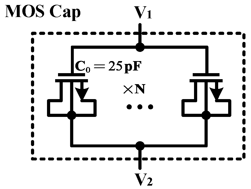
C10 are the active capacitors realized by the MOS capacitor, as depicted in Figure 10. Considered without peaking effect, the quality factor Q is set to 0.707 (Butterworth response). In this design, R9 = R10 and C9 = 2C10 = 200 pF.
To validate the tunable function of ActR, the binary-weighted reference resistor array is applied in the design. Figure 27 shows the plot of different frequency responses of the SKLPF with reference to that of benchmark implementation using an ideal resistor R. Their cut-off frequencies are summarized in Table 12.
As shown in Table 12, by tuning the resistance values of R9 and R10 within the range of 430.5 kΩ to 1.714 MΩ, fc is dynamically tuned from 0.627 kHz to 2.496 kHz. Additionally, the cutoff frequency fc of the Sallen–Key low-pass filter using the proposed ActR closely matches that of an ideal resistor. Across various tuning configurations, the deviation remains within 5%, with the maximum error being only 4.3%. The slight reduction in fc can be attributed to the intrinsic parasitic effects of the MOSFET-based ActR, which effectively increase the total capacitance in the circuit and slightly shift the frequency response downward. Despite this minor variation, the ActR maintains reasonable accuracy and reliability, particularly for low-frequency applications. The results have confirmed that the proposed tunable ActR can be a good replacement to a passive resistor in integrated filter design.
Taking routing area into account, the estimated layout area for each circuit block is stated in the following. They are summarized in Table 13. As can be seen, the active resistor core occupies approximately 150 × 35 μm2. The single op-amp consumes 30 × 20 μm2. The automatic tuning circuit with the binary-weighted reference resistor array is 150 × 35 μm2, and the DCP occupies 300 × 255 μm2. Hence, the overall layout area is approximately 0.096 mm2 or 320 μm × 300 μm. Of particular note is that the charge pump and the core tuning circuitry serve as the common resource of the tunable resistor system; the actual active resistor area is small and they can be applied on a large scale without requiring significant silicon area or power consumption.

5. Conclusions

This paper presents the design and implementation of a linear, tunable floating active resistor using the TSMC 40 nm CMOS process technology. The circuit incorporates several key circuits, such as the automatic tuning circuit for resistance stabilization against PVT variation, the active common-mode generator with utmost simplicity and drawing no current, the SCCT for quality level shifting, the triode-based native cascade transistors for reduced DC supply operation, and the DCP for generating the necessary boosted supply voltage.
The design has achieved good linearity performance as well as low power consumption. Due to the significantly low power in a single active resistor, it permits a large scale of active resistors to be implemented in integrated circuits and systems. Furthermore, the effective process sensitivity of the resistance and T.C. performance metrics are low. These technical merits make it attractive for precision analog circuit applications, such as voltage and current reference circuits, tunable sinusoidal oscillator, analog filters, programmable gain amplifiers and so forth. In brief, the proposed active resistor design offers a promising solution for realizing temperature-compensated and tunable resistors for advanced CMOS technology nodes.

Author Contributions

Conceptualization, Y.L. and P.K.C.; Validation: Y.L. and P.K.C.; Writing—Original Draft Preparation: Y.L.; Writing—Review and Editing: P.K.C. All authors have read and agreed to the published version of the manuscript.

Funding

This research received no external funding.

Institutional Review Board Statement

Not applicable.

Informed Consent Statement

Not applicable.

Data Availability Statement

Data are contained within the article.

Conflicts of Interest

The authors declare no conflicts of interest.

References

  1. Banu, M.; Tsividis, Y. Floating voltage-controlled resistors in CMOS technology. Electron. Lett. 1982, 18, 678–679. [Google Scholar] [CrossRef]
  2. Wilson, G.; Chan, P. Floating CMOS resistor. Electron. Lett. 1993, 29, 306–307. [Google Scholar] [CrossRef]
  3. Cavallaro, M.; Nicollini, G. An Active Resistor for Ultra Low Power Applications. IEEE Trans. Circuits Syst. I Regul. Pap. 2023, 70, 4418–4425. [Google Scholar] [CrossRef]
  4. Al-Absi, M.A.; Alkhulaifi, A. A MOS-Only Compact and Wide-Range Voltage-Controlled Grounded Resistor. J. Circuits Syst. Comput. 2024, 34, 2550096. [Google Scholar] [CrossRef]
  5. Wee, K.H.; Sarpeshkar, R. An electronically tunable linear or nonlinear MOS resistor. IEEE Trans. Circuits Syst. I Regul. Pap. 2008, 55, 2573–2583. [Google Scholar]
  6. Kledrowetz, V.; Haze, J.; Prokop, R.; Fujcik, L. An active resistor with a lower sensitivity to process variations, and its application in current reference. IEEE Access 2020, 8, 197263–197275. [Google Scholar] [CrossRef]
  7. Mahmoud, S. A Low Voltage CMOS Floating Resistor; IEEE: New York, NY, USA, 2004; pp. 453–456. [Google Scholar]
  8. Wilson, G.; Chan, P. Novel voltage-controlled grounded resistor. Electron. Lett. 1989, 25, 1725–1726. [Google Scholar] [CrossRef]
  9. Dave, M.; Baghini, M.S.; Sharma, D.K. A process and temperature compensated current reference circuit in CMOS process. Microelectron. J. 2012, 43, 89–97. [Google Scholar] [CrossRef]
  10. Zouaoui-Abouda, H.; Fabre, A. New high-value floating controlled resistor in CMOS technology. IEEE Trans. Instrum. Meas. 2006, 55, 1017–1020. [Google Scholar] [CrossRef]
  11. Magnelli, L.; Crupi, F.; Corsonello, P.; Pace, C.; Iannaccone, G. A 2.6 nW, 0.45 V temperature-compensated subthreshold CMOS voltage reference. IEEE J. Solid-State Circuits 2010, 46, 465–474. [Google Scholar] [CrossRef]
  12. Wang, Z. Novel voltage-controlled grounded resistor. Electron. Lett. 1990, 26, 1711–1712. [Google Scholar] [CrossRef]
  13. Temes, G.C. Analog MOS Integrated Circuits; Wiley: New York, NY, USA, 1988. [Google Scholar]
  14. Wang, Z. Current-controlled linear MOS earthed and floating resistors and their application. IEE Proc. G (Circuits Devices Syst.) 1990, 137, 479–481. [Google Scholar] [CrossRef]
  15. Ramírez-Angulo, J.; Carvajal, R.G.; Galán, J.A.; Lopez-Martin, A. A free but efficient low-voltage class-AB two-stage operational amplifier. IEEE Trans. Circuits Syst. II Express Briefs 2006, 53, 568–571. [Google Scholar] [CrossRef]
  16. Delbruck, T.; Mead, C.A. Adaptive photoreceptor with wide dynamic range. In Proceedings of the IEEE International Symposium on Circuits and Systems—ISCAS’94, London, UK, 30 May–2 June 1994; Volume 334, pp. 339–342. [Google Scholar]
  17. Harrison, R.R.; Charles, C. A low-power low-noise CMOS amplifier for neural recording applications. IEEE J. Solid-State Circuits 2003, 38, 958–965. [Google Scholar] [CrossRef]
  18. Delbrück, T.; Mead, C.A. Analog VLSI adaptive logarithmic wide-dynamic-range photoreceptor. In Proceedings of the IEEE International Symposium on Circuits and Systems, London, UK, 30 May–2 June 1994; pp. 339–342. [Google Scholar]
  19. Brito, T.M.; Colombo, D.M.; Moreno, R.L.; El-Sankary, K. CMOS Voltage Reference Using a Self-Cascode Composite Transistor and a Schottky Diode. Electronics 2019, 8, 1271. [Google Scholar] [CrossRef]
  20. Comer, D.J.; Comer, D.T.; Petrie, C.S. The utility of the composite cascode in analog CMOS design. Int. J. Electron. 2004, 91, 491–502. [Google Scholar] [CrossRef]
  21. Krummenacher, F.; Joehl, N. A 4-MHz CMOS continuous-time filter with on-chip automatic tuning. IEEE J. Solid-State Circuits 1988, 23, 750–758. [Google Scholar] [CrossRef]
  22. Silva-Martinez, J.; Steyaert, M.S.J.; Sansen, W. A 10.7-MHz 68-dB SNR CMOS continuous-time filter with on-chip automatic tuning. IEEE J. Solid-State Circuits 1992, 27, 1843–1853. [Google Scholar] [CrossRef]
  23. Banu, M.; Tsividis, Y. An elliptic continuous-time CMOS filter with on-chip automatic tuning. IEEE J. Solid-State Circuits 1985, 20, 1114–1121. [Google Scholar] [CrossRef]
  24. Prabhakar, G.; Vikram, A.; Pratap, R.; Singh, R. MOS capacitor based Dickson charge pump and ripple cancellation techniques using an LC circuit. Int. J. Knowl. Based Intell. Eng. Syst. 2020, 24, 311–321. [Google Scholar] [CrossRef]
  25. Carusone, T.C.; Johns, D.; Martin, K. Analog Integrated Circuit Design; John Wiley & Sons: Hoboken, NJ, USA, 2011. [Google Scholar]
  26. Ballo, A.; Grasso, A.D.; Giustolisi, G.; Palumbo, G. Optimized charge pump with clock booster for reduced rise time or silicon area. IEEE Trans. Circuits Syst. II Express Briefs 2019, 66, 1977–1981. [Google Scholar] [CrossRef]
  27. Ballo, A.; Grasso, A.D.; Palumbo, G. Dickson charge pump: Design strategy for optimum efficiency. In Proceedings of the 2021 19th IEEE International New Circuits and Systems Conference (NEWCAS), Toulon, France, 13–16 June 2021; pp. 1–4. [Google Scholar]
  28. Dickson, J.F. On-chip high-voltage generation in MNOS integrated circuits using an improved voltage multiplier technique. IEEE J. Solid-State Circuits 1976, 11, 374–378. [Google Scholar] [CrossRef]
  29. Ballo, A.; Grasso, A.D.; Palumbo, G. A review of charge pump topologies for the power management of IoT nodes. Electronics 2019, 8, 480. [Google Scholar] [CrossRef]
  30. Mal, A.K.; Todani, R. Non Overlapping Clock generator for switched capacitor circuits in Bio-Medical applications. In Proceedings of the 2011 International Conference on Signal Processing, Communication, Computing and Networking Technologies, Thuckalay, India, 21–22 July 2011; pp. 238–243. [Google Scholar]
  31. Chen, H.; Chan, P.K. A Low-Voltage Low-Power Voltage-to-Current Converter with Low Temperature Coefficient Design Awareness. Sensors 2025, 25, 1204. [Google Scholar] [CrossRef]
  32. Yucel, F.; Yuce, E. A new electronically fine tunable grounded voltage controlled positive resistor. IEEE Trans. Circuits Syst. II Express Briefs 2017, 65, 451–455. [Google Scholar] [CrossRef]
  33. Yadav, H.; Bansal, U.; Senani, R. New electronically fine-tunable CMOS floating resistor configuration and its application. AEU-Int. J. Electron. Commun. 2025, 192, 155690. [Google Scholar] [CrossRef]
  34. Sallen, R.P.; Key, E.L. A practical method of designing RC active filters. IRE Trans. Circuit Theory 1955, 2, 74–85. [Google Scholar] [CrossRef]
Figure 1. Floating voltage-controlled active resistor.
Chips 04 00018 g001
Figure 2. Floating active resistor with common-mode generator incorporating bulk effect.
Chips 04 00018 g002
Figure 3. Grounded active resistor with pre-distortion compensation.
Chips 04 00018 g003
Figure 4. Schematic of proposed floating active resistor.
Chips 04 00018 g004
Figure 5. (a) Vth vs. VSB of native, LVT and HVT transistors; (b) γ vs. VSB of native, LVT and HVT transistors.
Chips 04 00018 g005
Figure 6. Common-mode voltage VCM generation.
Chips 04 00018 g006
Figure 7. Plot of respective leakage current nA in each PR against input voltage variation.
Chips 04 00018 g007
Figure 8. Common-mode voltage VCM against input voltage.
Chips 04 00018 g008
Figure 9. Proposed automatic tuning circuit.
Chips 04 00018 g009
Figure 10. MOS capacitor with deep N-well.
Chips 04 00018 g010
Figure 11. Schematic of op-amp.
Chips 04 00018 g011
Figure 12. CMRR, PSRR and open-loop gain of the op-amp.
Chips 04 00018 g012
Figure 13. Output voltage of DCP.
Chips 04 00018 g013
Figure 14. Schematic diagram of DCP with MOS capacitors.
Chips 04 00018 g014
Figure 15. (a) Ring oscillator; (b) non-overlapping clock generator.
Chips 04 00018 g015
Figure 16. The 2nd-order low-pass filter.
Chips 04 00018 g016
Figure 17. Resistance under DCP: (a) @TT Corner, (b) @SS Corner, (c) @FF Corner, (d) @SF Corner, (e) @FS Corner.
Chips 04 00018 g017
Figure 18. Resistance vs. Vin without tuning circuit: (a) @−25 °C, (b) @0 °C, (c) @27 °C, (d) @85 °C.
Chips 04 00018 g018
Figure 19. Resistance vs. Vin with tuning circuit: (a) @−25 °C, (b) @0 °C, (c) @27 °C, (d) @85 °C.
Chips 04 00018 g019aChips 04 00018 g019b
Figure 20. Resistance vs. temperature without tuning circuit: (a) @ V 1 V 2 = ± 0.25   V ; (b) @ V 1 V 2 = ± 0.5   V ; (c) @ V 1 V 2 = ± 0.75   V .
Chips 04 00018 g020
Figure 21. Resistance vs. temperature with tuning circuit: (a) @ V 1 V 2 = ± 0.25   V ; (b) @ V 1 V 2 = ± 0.5   V ; (c) @ V 1 V 2 = ± 0.75   V .
Chips 04 00018 g021
Figure 22. MC simulations of resistance: (a) @TT corner, (b) @SS corner, (c) @FF corner, (d) @SF corner, (e) @FS corner.
Chips 04 00018 g022
Figure 23. MC simulations of T.C.: (a) @TT corner, (b) @SS corner, (c) @FF corner, (d) @SF corner, (e) @FS corner.
Chips 04 00018 g023
Figure 24. Binary-weighted reference resistor array implementation.
Chips 04 00018 g024
Figure 25. Change of ActR resistance against frequency.
Chips 04 00018 g025
Figure 26. Tunable Sallen–Key low-pass filter.
Chips 04 00018 g026
Figure 27. Frequency responses of tunable Sallen–Key low-pass filter with ideal resistors and tunable active resistors.
Chips 04 00018 g027
Table 1. Device types and sizes of the proposed active resistor.
ComponentModelSize (W/L)Multiplier
M1–2nch_na25_mac1.5/200 (µm/µm)1
M3–6pch_25_mac120/600 (nm/nm)5
M7–8pch_25_mac0.5/10 (µm/µm)1
M9pch_25_mac2/8 (µm/µm)1
M10pch_25_mac1.8/8 (µm/µm)1
M11pch_25_mac16/4 (µm/µm)1
Table 2. Size of components in automatic tuning.
ComponentModelSize (W/L)Multiplier
M9pch_25_mac2 µm/8 µm10
M10pch_25_mac1.86 µm/8 µm3
M11pch_25_mac16 µm/4 µm10
R1rnpoly_wo68 kΩ-
R2rppoly_wo185 kΩ-
C0nch_25_dnw_mac50/45 (µm/µm) 25 pF1
C1–2nch_25_dnw_mac4 × C0 = 100 pF4
Table 3. Size of components in op-amp.
ComponentModelSize (W/L)Multiplier
MN1–2nch_25_mac8 µm/2 µm4
MN3–4nch_25_mac2 µm/1 µm1
MP1–2pch_25_mac2 µm/4 µm1
MP3–5pch_25_mac8 µm/4 µm1
MP6–7pch_25_mac500 nm/1 µm1
R3rnpoly_wo28 kΩ-
R4rppoly_wo72 kΩ-
Table 4. Device types and their sizes used in the DCP.
ComponentModelSize (W/L)Multiplier
M12–16nch_dnw_mac50/1 (µm/µm)10
NAND1–2pch_mac & nch_mac120/40, 120/40 (nm/nm)1
Inv1–3pch_mac & nch_mac2.5/1.5, 1/5 (µm/µm)1
Inv4–6pch_mac & nch_mac120/40, 120/40 (nm/nm)1
Inv7–8pch_mac & nch_mac1/40, 1/40 (µm/nm)1
Inv9–10pch_mac & nch_mac4/40, 4/40 (µm/nm)1
Inv11–12pch_mac & nch_mac28/0.04, 28/0.04 (µm/µm)1
C3–6nch_25_dnw_mac4 × C0 = 100 pF4
C7–8nch_25_dnw_mac8 × C0 = 200 pF8
R5–8rnpoly_wo1 kΩ-
RLrnpoly_wo250 kΩ-
ILCurrent Source9.5 µA-
Table 5. Simulated linearity FOM without and with automatic tuning circuit.
Linearity FOM (V−1)Without Tuning CircuitWith Tuning Circuit
T e m p = 25   ° C 2.1 × 10 2 2.8 × 10 2
T e m p = 0   ° C 1.7 × 10 2 2.6 × 10 2
T e m p = 27   ° C 2.5 × 10 2 2.4 × 10 2
T e m p = 85   ° C 2.6 × 10 2 3.1 × 10 2
Table 6. Simulated T.C. performance without and with automatic tuning circuit.
T.C. (ppm/°C)Without Tuning Circuitwith Tuning Circuit
V 1 V 2 = 0.25   V 4.264 × 10 3 44.02
V 1 V 2 = 0.25   V 4.262 × 10 3 44.17
V 1 V 2 = 0.5   V 4.270 × 10 3 57.28
V 1 V 2 = 0.5   V 4.266 × 10 3 57.45
V 1 V 2 = 0.75   V 4.271 × 10 3 61.36
V 1 V 2 = 0.75   V 4.271 × 10 3 61.23
Table 7. ActR values under different process corners with automatic tuning.
TTSSFFSFFS
σ (Ω)5.72 k6.93 k4.48 k5.75 k5.68 k
μ (Ω)887.41 k1.05 M716.19 k886.63 k888.20 k
σ/μ (%)0.640.660.620.640.64
Table 8. T.C. variation at different process corners with automatic tuning circuit.
TTSSFFSFFS
σ (ppm/°C)10.0210.649.3410.229.83
μ (ppm/°C)57.0854.1661.6159.0255.56
σ/μ (%)17.5519.6415.1517.3217.69
Table 9. Device types and sizes of the binary-weighted reference resistor array.
ComponentModelSize (W/L)
RArray1arnpoly_wo16.15 kΩ
RArray1brppoly_wo46.35 kΩ
RArray1/Runitrnpoly_wo + rppoly_wo62.5 kΩ
RArray2rnpoly_wo + rppoly_wo125 kΩ
RArray4rnpoly_wo + rppoly_wo250 kΩ
RArray8rnpoly_wo + rppoly_wo500 kΩ
SW1nch_hvt_dnw32 µm/1 µm
SW2nch_hvt_dnw32 µm/1 µm
SW4nch_hvt_dnw48 µm/1 µm
SW8nch_hvt_dnw68 µm/1 µm
Table 10. Performance comparison with previously reported works.
Unit2008201220182020202320252025
[5][9][32][6][3][33]This Work #
Process TechnologynmNA18025018013018040
DC SupplyVNA1.81.251.51.21.251
Typical ActR Value250.120.0010.0520.30.0520.89
Res. Tuning RangeNA1 × 103~
1 × 10⁶
0.77~
1.37
NANA35.73~
71.26
430.5~
1.714 × 10³
Single ActR
Transistor Count
NA23106612188
1 Res. Sen.(σ/μ) %NA1.33NANA4.9NA0.14
2 Res. Sen.(σ/μ) %NANANA1.6NANA0.64
Temp. Range°C6~460~100−25~75−20~85−40~125−20~40−25~85
1 T.C.ppm/°CNA4400NANA300057004300
1 T.C. Sen.(σ/μ) %NANANANANANA0.06
2 T.C.ppm/°C4000NANA500NANA57
2 T.C. Sen.(σ/μ) %NANANANANANA17.55
1 Linearity FOMV−1NANANANA2.1 × 10−1NA2.5 × 10−2
2 Linearity FOMV−1NANANA3.2 × 10−2NANA2.4 × 10−2
ActR Bias Control CurrentnA5 × 103NANA10 × 1033.540 × 103121
Single ActR Power ConsumptionμWNANANA154.2 × 10−350* 0.25
1 without tuning circuit; 2 with tuning circuit; # with the use of native transistors as ActR; * with 2.1 V typical bootstrapped supply voltage of ActR from DC input of 1 V.
Table 11. T.C. of passive resistor and loop gain of loop2 variation at different process corners with automatic tuning circuit.
TTSSFFSFFS
T.C. of Passive R (ppm/°C)14.7614.4815.3114.7614.76
Loop Gain of Loop2 (dB)61.2764.757.964.557.8
T.C. of ActR (ppm/°C)57.0854.1661.6159.0255.56
Table 12. Cutoff frequencies of the Sallen–Key low-pass filter with ideal resistors and tunable active resistors.
Rarray1 = 62.5 kΩRarray1 = 125 kΩRarray1 = 250 kΩRarray1 = 500 kΩ
ActR Resistance (kΩ)430.5609.6887.41.714 × 103
fc of Ideal R (kHz)2.6031.8341.2660.655
fc of ActR (kHz)2.4961.7661.2230.627
Error (%)4.13.73.44.3
Table 13. Cutoff frequency fc of the Sallen–Key low-pass filter with ideal resistors and tunable active resistors.
BlockActive Resistor CoreSingle Op-AmpAuto-Tuning CircuitDickson Charge Pump
Estimated Area (μm × μm)150 × 530 × 20150 × 35300 × 255
Disclaimer/Publisher’s Note: The statements, opinions and data contained in all publications are solely those of the individual author(s) and contributor(s) and not of MDPI and/or the editor(s). MDPI and/or the editor(s) disclaim responsibility for any injury to people or property resulting from any ideas, methods, instructions or products referred to in the content.

