1. Introduction
The increasing demand for compact, low-power infrared (IR) sensors has become a driving force in the development of wearables, mobile devices, IoT applications, and even low-cost thermal imagers and multi-spectral Focal Plane Arrays (FPAs) [
1,
2,
3]. Traditional IR sensing techniques, however, frequently encounter significant hurdles related to size constraints, power consumption, and the complexities of semiconductor integration. To overcome these limitations, developers have introduced Thermal Metal-Oxide-Semiconductor (TMOS) technology [
4]. Leveraging advanced CMOS-SOI-MEMS platforms, manufacturers of TMOS devices offer a compelling solution by providing high sensitivity and low power consumption, all while maintaining compatibility with established microelectronics fabrication processes [
5].
A critical pathway to further enhance the performance of TMOS and other thermal-IR sensors lies in optimizing the spectral selectivity and optical efficiency of their absorbing layers. The direct integration of narrowband, highly efficient optical filters immediately above the sensor can substantially boost responsivity and improve overall signal-to-noise ratios. This approach is particularly critical for achieving narrow bandpass absorption, which enhances the sensor’s ability to selectively detect specific wavelengths of infrared radiation. Furthermore, such spectrally selective pixels may enable the detection of temperature and emissivity of object surfaces [
6,
7]. Unfortunately, conventional optical filters often prove impractical due to their bulkiness or inherent incompatibility with standard CMOS fabrication workflows, making it very challenging to achieve on-chip spectral selectivity within a single device. Therefore, an external optical filter is usually integrated into the sensor package rather than directly within the sensor device layers, which in turn contributes to a bulkier and more expensive sensor package.
In this context, metal–insulator–metal (MIM) metasurfaces emerge as a highly attractive alternative. These subwavelength structures are engineered to produce precise optical responses, including strong absorption and spectral filtering, within an ultra-thin, planar configuration. Crucially, MIM metasurfaces can be monolithically integrated into the same CMOS-SOI layer as the TMOS device itself, thereby enabling the realization of flat optics with minimal additional cost and footprint.
Nevertheless, the design of these structures to meet specific spectral requirements, particularly within the long-wave infrared (LWIR) region, presents notable challenges. While full-wave electromagnetic solvers provide highly accurate results, their application is often computationally intensive and offers limited intuitive guidance for the design process. Consequently, equivalent-circuit models have gained prominence as a alternative for gaining design intuition in MIM absorber development, especially for mid-IR and LWIR (2–14 μm) applications. These models not only provide valuable insight into design parameters but also drastically reduce the need for extensive simulation-based parameter sweeps, leading to significant time savings.
This work presents a new approach for the methodology of designing MIM absorbers in the mid-infrared and long-wave infrared (LWIR) regions, utilizing the intuitive insights provided by equivalent circuit modeling. The methodology is demonstrated and validated through inverted cross dipole designs that achieve spectral selectivity in the LWIR region (8–14 μm).
2. Background and Related Work
2.1. CMOS-SOI-MEMS Thermal Sensor Technology Fundamentals
The development of low-cost, compact, and efficient IR sensors has been significantly advanced by CMOS-SOI-MEMS (Complementary Metal-Oxide-Semiconductor Silicon-On-Insulator Micro-Electro-Mechanical Systems) technology [
8]. A notable innovation within this domain is the Thermal Metal-Oxide-Semiconductor (TMOS) sensor [
5]. Unlike traditional uncooled IR technologies such as bolometers, thermopiles, and pyroelectric sensors, TMOS leverages a suspended, micro-machined, thermally insulated transistor to directly convert absorbed infrared radiation into an electrical signal [
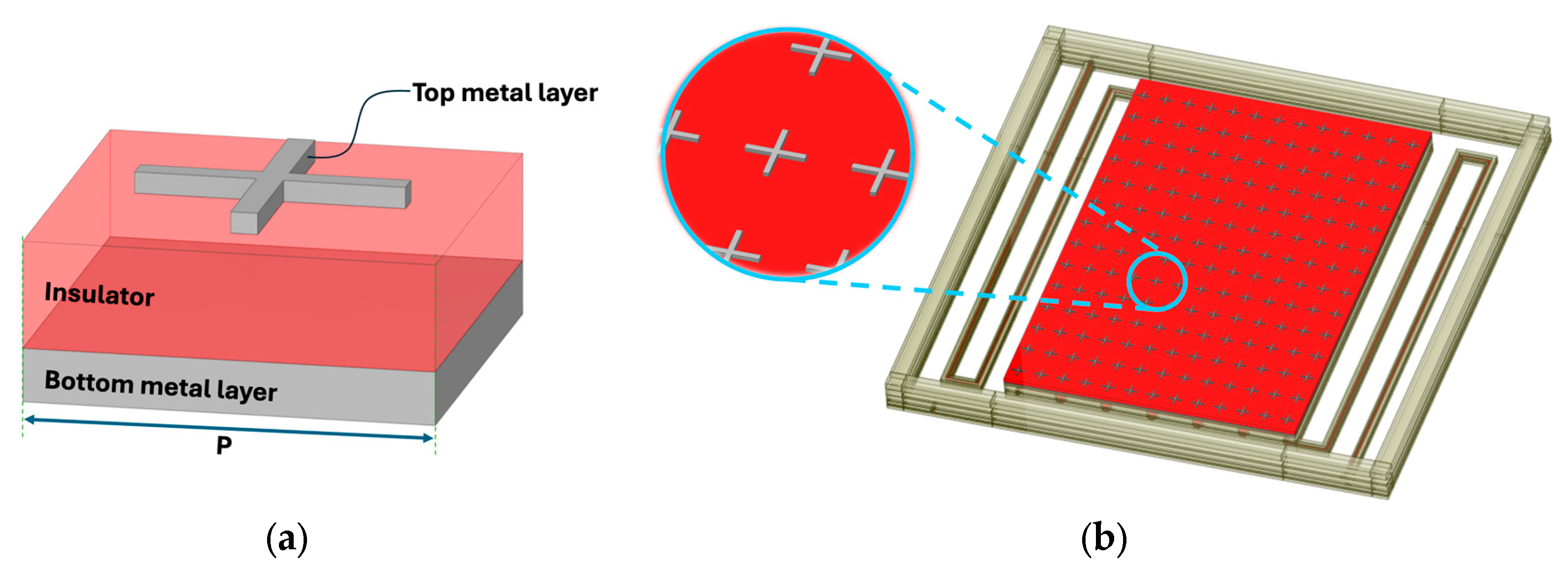
9]. This unique architecture, illustrated schematically in
Figure 1, allows TMOS technology devices to operate effectively in the subthreshold regime, offering significant advantages including ultra low power consumption (in the micro-Watt range) and high temperature sensitivity. The compatibility of TMOS with standard CMOS-SOI fabrication processes is crucial, enabling miniaturization and cost-effective production, particularly through wafer-level processing and packaging (WLP) [
10].
2.2. Metamaterial Absorbers in IR Applications
Recent advancements in materials science have introduced metamaterials, artificially constructed structures engineered to exhibit electromagnetic properties not found in naturally occurring materials [
11,
12,
13,
14]. Among these, meta-absorbers are specifically designed to optimize the absorption of incident electromagnetic radiation. Their unique electromagnetic characteristics offer a promising solution to the challenge of balancing miniaturization with sensor sensitivity in IR systems. By strategically integrating metamaterials into sensor architectures, it is possible to develop compact, high-sensitivity IR systems for diverse applications.
A particularly attractive class of meta-absorbers for IR applications are metal–insulator–metal (MIM) metasurfaces. These structures typically consist of a thin dielectric layer sandwiched between two metal layers, with the top layer patterned into sub-wavelength structures such as squares, circles, or other shapes [
15]. The patterned top metal layer interacts with incident radiation, supporting localized surface plasmon resonances, which may couple to different types of resonances, which concentrate the electromagnetic field within the dielectric layer, leading to high absorption and spectral filtering within a thin, planar configuration. For effective absorption, the design should incorporate a high density of MIM units, implying that the periodicity (P) should be as small as possible, leading to many periods within the sensor area (See
Figure 2).
2.3. Full-Wave Simulation Methods
Designing MIM metasurfaces for specific spectral requirements, particularly in the long-wave infrared (LWIR) region, presents significant challenges. Full-wave electromagnetic solvers, such as those based on the Finite-Difference Time-Domain (FDTD) method (e.g., Ansys Lumerical [
16]) or Finite Element Methods (FEM), provide highly accurate results by solving Maxwell’s equations in complex geometries. FDTD, for instance, operates in the time domain, allowing for broadband results from a single simulation, and is well-suited for simulating very thin layers with precise frequency-dependent refractive indices. FEM, conversely, solves equations in the frequency domain, making it more suitable for high-Q circuits and resonators [
17].
However, these full-wave simulations are often computationally intensive, requiring substantial resources and offering limited intuitive understanding of the design process. To address this, equivalent-circuit models have emerged as an alternative for gaining design intuition in MIM absorber development. These models simplify the complex electromagnetic interactions into an equivalent electrical circuit, providing a more intuitive understanding of how design parameters influence the optical response. This approach can drastically reduce the need for extensive simulation-based parameter sweeps, thereby saving considerable time during the design phase while still offering valuable insights into the underlying physics. While full-wave simulations remain essential for final validation and fine-tuning, equivalent-circuit models provide an efficient and insightful pathway for initial design and optimization, particularly for mid-IR and LWIR (2–14 microns) applications [
3,
18].
3. Perfect Absorption and Transmission Line Circuit Model
The electromagnetic behavior of the MIM absorber can be effectively analyzed using a transmission line circuit model, as illustrated in
Figure 3. This approach provides physical insight into the absorption mechanism and enables straightforward design optimization.
The MIM structure is modeled as a transmission line circuit consisting of two main components. Surface impedance,
Zs, represents the patterned metallic resonator layer and Transmission line stub, which represents the dielectric spacer layer backed by the ground plane (see
Figure 3).
The surface impedance characterizes the electromagnetic response of the patterned metal layer as a thin resistive sheet. This impedance captures both the resistive losses (responsible for absorption) and reactive components (determining resonance frequency) of the metallic pattern.
The dielectric layer of thickness acts as a transmission line stub terminated by a short circuit (the ground plane). This stub presents an input impedance that depends on the electrical thickness of the dielectric layer.
The total input impedance
seen from the free-space interface is given by the parallel combination of the surface impedance and the transformed stub impedance [
3,
19]:
Therefore, extracting
:
is the characteristic impedance of the dielectric layer, is the propagation constant in the dielectric, is the thickness of the dielectric layer, and is the refractive index of the dielectric material.
The parallel connection represents two current paths available to the incident electromagnetic wave. Direct path through the metal pattern: Current flows directly through the patterned metal, experiencing the surface impedance . And Cavity path: Current flows through the dielectric cavity to the ground plane, experiencing the transformed impedance .
Both paths experience the same voltage (electric field), while their currents add to give the total response. This parallel combination determines the overall reflection and absorption characteristics of the structure.
Perfect absorption (zero reflection) occurs when the input impedance matches the free space impedance [
19,
20]:
This matching condition can be achieved by proper design of both the metal pattern (controlling ) and the dielectric cavity dimensions (controlling the stub impedance).
At resonance, when approaches infinity, the stub impedance becomes very large, and the input impedance approaches . For perfect absorption at resonance, the surface impedance should equal the free space impedance:
This circuit model enables rapid design optimization without requiring full-wave electromagnetic simulations, making it particularly valuable for engineering applications.
The quality factor (Q-factor) is a crucial parameter for characterizing the spectral selectivity of the absorber. It quantifies the sharpness of the resonance peak, with higher Q-factors indicating a narrower bandpass absorption. The Q-factor can be defined as [
20,
21]:
where
is the resonance wavelength, and Δ
λ is the full width at half maximum (FWHM) of the absorption peak. In terms of design guidelines for MIM absorbers, the length of the dipole or the overall pattern geometry primarily determines the resonance wavelength (
). A good starting point to determine
is that the length of the dipole should be approximately:
where
is the dipole length and
is the effective refractive index surrounding the top pattern layer. Furthermore, the width of the patterned elements plays a critical role in controlling the effective impedance, which is essential for achieving optimal absorption and impedance matching with free space.
4. Absorber Design Methodology and Numerical Simulations
In this study, we investigate a complementary (inverted) cross-dipole structure. The unit cell shape is designed to be C4 symmetric to ensure less sensitivity to polarization and angle of incident variations [
22,
23]. To estimate the effective index
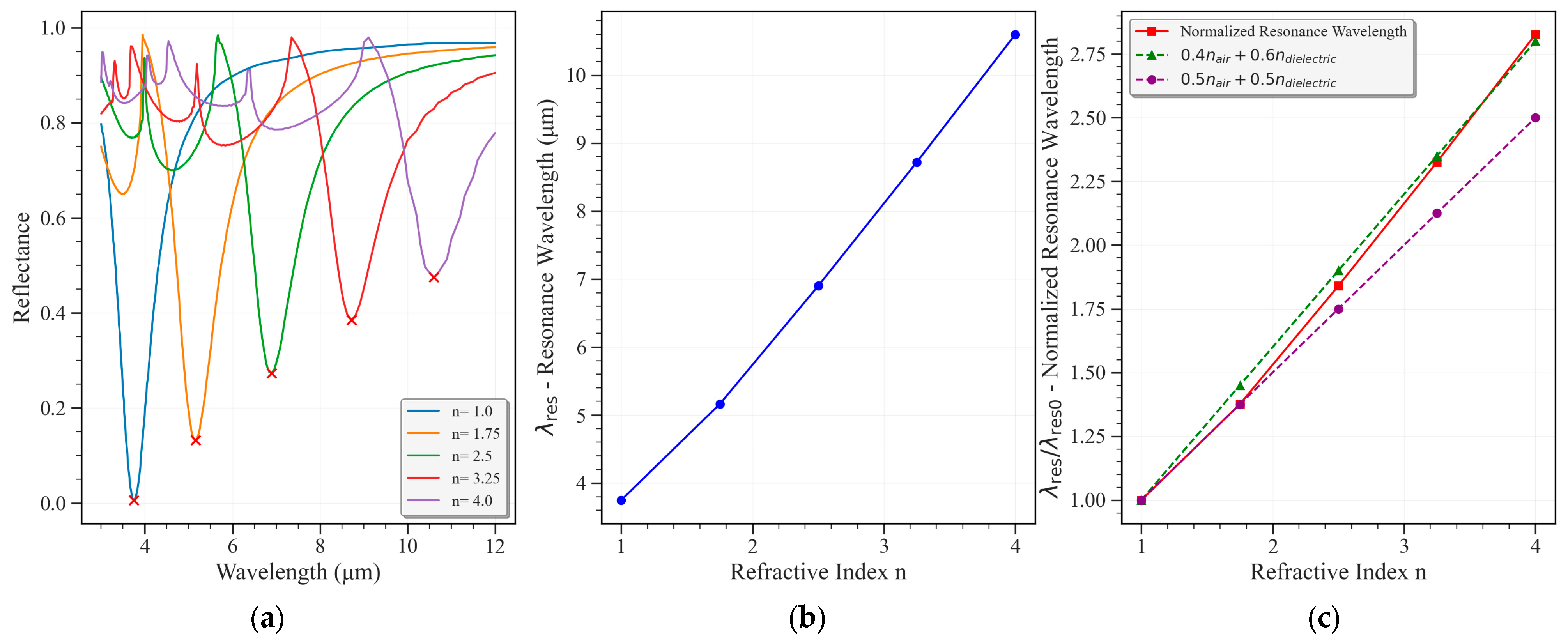
for Equation (5), we simulate an etched cross-dipole aperture with arm length 1.7 μm and width 0.3 μm (see
Figure 4). The metal film is aluminum with a thickness of 0.1 μm. The refractive index data for aluminum was obtained from the Lumerical material library, which is based on the CRC Handbook of Chemistry and Physics [
24]. The structure is simulated without a bottom metallic reflector, so the complementary cross-dipole supports localized surface plasmon resonances (LSPRs) and transmits the incident radiation through the aperture.
When the substrate refractive index differs from that of free space, impedance mismatch occurs. Without adjusting the cross-dipole geometry to account for this mismatch, a portion of the incident radiation is reflected, reducing transmission and modifying the resonance response.
Figure 5 exhibits the results for varying value of the substrate refractive index [
16].
Figure 5 demonstrates that an increase in the substrate’s refractive index leads to a redshift in the resonance wavelength. This redshift can be approximated by a linear relationship, where
represents the resonance wavelength when the metallic pattern is surrounded by free space, and
is the refractive index of free space—
.
These findings suggest that a high refractive index substrate is advantageous for achieving a small period in the meta-absorber units. Consequently, silicon was selected as the dielectric material for this study due to its relatively high refractive index, , compared to other dielectric materials available in standard CMOS-SOI fabrication facilities. Furthermore, silicon exhibits negligible losses, which also contribute to higher Q-factor, within the mid and long-infrared regions (2–14 microns), making it an ideal choice for this application.
Following the selection of the dielectric substrate, several designs were tested and simulated within the complete MIM meta-absorber structure, including the bottom reflector metal layer.
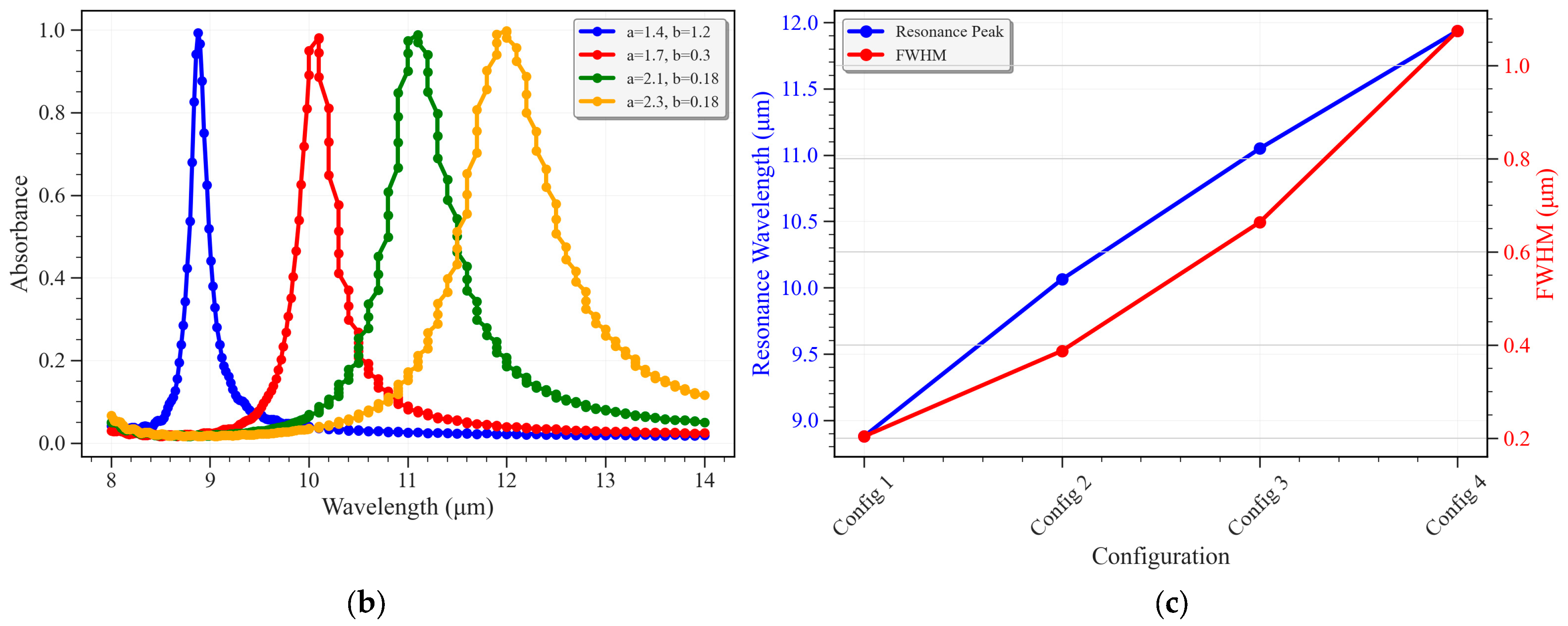
Figure 6 presents the chosen designs, along with their unit dimensions, which achieve near-perfect and selective absorption in the LWIR region, 8–14 microns.
As depicted in
Figure 6, a series of optimized metamaterial absorber designs were investigated to achieve selective absorption in the long-wave infrared (LWIR) region.
Figure 6b presents the simulated absorbance spectra for each of the four configurations. All designs exhibit near-perfect absorption, with peak absorbance values exceeding 95% in the LWIR range.
A clear redshift in the resonance wavelength is observed as the dimensions of the top metallic pattern are varied from Config 1 to Config 4. Specifically, Config 1 shows a resonance at approximately 8.88 μm, while Config 4 resonates at around 12 μm. This tunability of the resonance wavelength across the LWIR spectrum is critical for applications requiring selective thermal emission or sensing.
The observed spectral shifts are directly correlated with the changes in the geometric parameters,
and
, of the cross-shaped metallic resonators, as detailed in
Figure 6a. For instance, increasing the arm length
and modifying the arm width
effectively alters the resonant conditions of the plasmonic modes supported by the structures, leading to the observed redshift. This demonstrates the precise control over the absorption wavelength achievable through geometric engineering of the unit cell.
Figure 7 presents the calculated real and imaginary components of
for the four different metamaterial configurations. These results are crucial for understanding the individual contributions of the patterned metallic layer to the overall absorption mechanism and for validating the transmission line model. The peak in the real part of
at the resonance wavelength indicates the maximum resistive loss, which is essential for efficient absorption. The plots for
show how the patterned layer’s impedance contributes to achieving this critical impedance matching condition at different resonance wavelengths.
Beyond the top pattern geometry, the thickness of the dielectric spacer layer (h) plays an equally crucial role in tuning the absorption characteristics and achieving impedance matching. As shown in
Figure 8, varying the dielectric thickness significantly impacts both the resonance wavelength and the overall absorption efficiency. The contour plot illustrates how specific combinations of wavelength and dielectric thickness lead to minimal reflectance (high absorption), forming distinct absorption bands. This highlights the importance of precisely controlling the dielectric layer thickness during fabrication to ensure optimal performance at the desired operating wavelength.
5. Discussion
This study successfully investigated the design and performance of CMOS-compatible MIM metamaterial absorbers for selective absorption in the LWIR region, with a specific focus on their integration with TMOS sensors. The equivalent-circuit model proved to be a potentially useful tool, offering significant physical insight into the absorption mechanism and enabling efficient design optimization, thereby substantially reducing the computational burden typically associated with full-wave electromagnetic simulations.
Our findings underscore the critical role of the dielectric substrate’s refractive index in determining the absorber’s spectral response. The observed linear redshift in resonance wavelength with increasing substrate refractive index (
Figure 5) highlights the tunability offered by material selection. The strategic choice of silicon as the dielectric material was justified by its high refractive index, which facilitates smaller unit cell periods for high-density integration, and its negligible optical losses in the 2–14 μm range, contributing to a higher quality factor (Q-factor) and enhanced spectral selectivity.
Through systematic design variations, we demonstrated precise control over the absorption characteristics.
Figure 7a clearly illustrates that by modifying the geometric parameters (
and
) of the top metallic patterns, the resonance wavelength can be effectively tuned across the LWIR spectrum, achieving near-perfect absorption (exceeding 95%) for all optimized configurations. This geometric engineering directly influences the plasmonic modes supported by the structures, leading to the observed spectral shifts and maintaining narrow FWHM values, indicative of high spectral selectivity.
A common characteristic observed in resonant systems, including these metamaterial absorbers, is that redshifting the resonance wavelength often leads to a larger FWHM. This phenomenon can be understood in terms of the Q-factor, defined as . As the resonance wavelength (λres) increases, the physical dimensions of the resonant structures also typically increase. This larger physical size can lead to increased radiative losses or enhanced ohmic losses over a greater volume, which in turn broadens the spectral response (Δλ). While the Q-factor may remain relatively constant or decrease slightly, an increase in λres necessitates a corresponding increase in Δλ to maintain the relationship, thereby resulting in a broader absorption peak. Despite this general trend, the designs presented here maintain sufficiently narrow FWHM values, underscoring their suitability for selective sensing applications.
6. Conclusions
This work presents a comprehensive approach and methodology for the design of high-performance MIM metamaterial absorbers tailored for long-wave infrared (LWIR) applications, utilizing an efficient equivalent-circuit approach validated by full-wave simulations. Silicon was identified as an optimal dielectric substrate, owing to its high refractive index and low intrinsic losses, enabling compact geometries and spectrally selective responses. By carefully engineering the metallic pattern dimensions, precise control over the absorption wavelength and spectral selectivity was achieved, yielding near-unity absorption across the LWIR band. Furthermore, the transmission-line circuit model offered valuable physical insight into the impedance-matching conditions critical for achieving strong absorption. These results highlight the potential for monolithic integration of spectrally selective optical filters directly onto CMOS–SOI–MEMS TMOS sensors, offering a pathway toward miniaturized, cost-effective, and functionally enhanced next-generation infrared sensing systems.


