
Electron. Mater., Volume 6, Issue 2 (June 2025) – 4 articles
Cover Story (view full-size image):
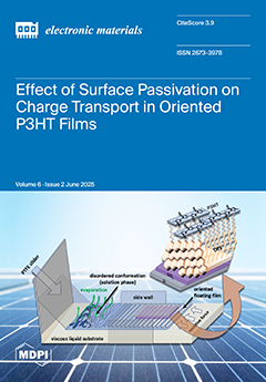
Flexible and wearable electronics based on organic materials are vital for future technologies but are often limited by inefficient charge transport. Researchers at the Kyushu Institute of Technology addressed this by studying how surface passivation affects charge transport in oriented RR-P3HT thin films. Using the Floating Film Transfer Method (FTM), RR-P3HT films were deposited on SiO2 substrates modified with OTS-based SAMs. The optimized OTS layer, treated with octadecene at high temperatures (OTS-F), reduced interface traps, enhanced film orientation, and promoted edge-on stacking. Notably, charge carrier mobility reached 0.18 cm2/V−1s−1. Optical, structural, and electrical characterizations confirmed that interfacial engineering, crystallinity, and molecular alignment are key to improving OFET performance. View this paper
- Issues are regarded as officially published after their release is announced to the table of contents alert mailing list.
- You may sign up for e-mail alerts to receive table of contents of newly released issues.
- PDF is the official format for papers published in both, html and pdf forms. To view the papers in pdf format, click on the "PDF Full-text" link, and use the free Adobe Reader to open them.
Previous Issue
Next Issue