Next Issue
Volume 7, March
Previous Issue
Volume 6, September


Electron. Mater., Volume 6, Issue 4 (December 2025) – 11 articles

Cover Story (view full-size image): 
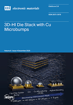
This cover captures the shift from transistor scaling to system-level integration through advanced packaging. A 3D heterogeneous die stack and interconnect evolution illustrate microbump scaling below 5 µm interconnect pitch. The design reflects comprehensive modeling of thermal cycling, intermetallic growth, fatigue-creep and thermal performance analysis of solder-based thermo-compression bonding (TCB) and Cu–Cu TCB. The paper highlights the markedly superior reliability and lifetime of Cu–Cu thermo-compression bonding compared to conventional solder-based off-chip interconnections. View this paper
  • Issues are regarded as officially published after their release is announced to the table of contents alert mailing list.
  • You may sign up for e-mail alerts to receive table of contents of newly released issues.
  • PDF is the official format for papers published in both, html and pdf forms. To view the papers in pdf format, click on the "PDF Full-text" link, and use the free Adobe Reader to open them.
Order results
Result details
Select all
Export citation of selected articles as:
20 pages, 3397 KB  
Article
Image Enhancement Algorithm and FPGA Implementation for High-Sensitivity Low-Light Detection Based on Carbon-Based HGFET
by Yi Cao, Yuyan Zhang, Zhifeng Chen, Dongyi Lin, Chengying Chen, Liming Chen and Jianhua Jiang
Electron. Mater. 2025, 6(4), 23; https://doi.org/10.3390/electronicmat6040023 - 2 Dec 2025
Viewed by 204
Abstract
To address the issues of insufficient responsivity and low imaging contrast of carbon-based HGFET high-sensitivity short-wave infrared (SWIR) detectors under low-light conditions, this paper proposes a high-sensitivity and high-contrast image enhancement algorithm for low-light detection, with FPGA-based hardware verification. The proposed algorithm establishes [...] Read more.
To address the issues of insufficient responsivity and low imaging contrast of carbon-based HGFET high-sensitivity short-wave infrared (SWIR) detectors under low-light conditions, this paper proposes a high-sensitivity and high-contrast image enhancement algorithm for low-light detection, with FPGA-based hardware verification. The proposed algorithm establishes a multi-stage cooperative enhancement framework targeting key challenges such as low signal-to-noise ratio (SNR), high dark-state noise, and weak target extraction. Unlike traditional direct enhancement methods, the proposed approach first performs defective row-column correction and background noise separation based on dark-state data, which provides a clean foundation for signal reconstruction. Furthermore, an adaptive gamma correction mechanism based on image maximum value is introduced to avoid unnecessary nonlinear transformations in high-contrast regions. During the contrast enhancement stage, an exposure-constrained adaptive histogram equalization strategy is adopted to effectively suppress noise amplification and saturation in low-light scenes. Finally, an innovative dual-mode threshold selection method based on image variance is proposed, which can dynamically integrate the OTSU algorithm with statistical moment analysis to ensure robust background noise separation across both high- and low-contrast scenarios. Experimental results demonstrate that the proposed algorithm significantly improves target contrast in infrared images while preventing detail loss due to overexposure. Under microwatt-level laser power, background noise is effectively suppressed, and both imaging quality and weak target detection capability are substantially enhanced. Full article
Show Figures

Figure 1

15 pages, 2561 KB  
Article
Integration of Silicon PIN Detectors and TENGs for Self-Powered Wireless AI Intelligent Recognition
by Junjie Tang, Huafei Wang, Maoqiu Pu, Penghui Luo, Min Yu and Zhiyuan Zhu
Electron. Mater. 2025, 6(4), 22; https://doi.org/10.3390/electronicmat6040022 - 2 Dec 2025
Viewed by 228
Abstract
In this study, we explore the integration of a cost-effective triboelectric nanogenerator (TENG) with an large silicon PIN detector (diameter: 12 mm) for intelligent wireless recognition applications. Wireless communication eliminates the need for physical connections, enabling greater flexibility and scalability in deployment. It [...] Read more.
In this study, we explore the integration of a cost-effective triboelectric nanogenerator (TENG) with an large silicon PIN detector (diameter: 12 mm) for intelligent wireless recognition applications. Wireless communication eliminates the need for physical connections, enabling greater flexibility and scalability in deployment. It allows for seamless integration of AI systems into a wide range of environments without the constraints of wiring, reducing installation complexity and enhancing mobility. Additionally, we demonstrate the TENG’s functionality as an autonomous communication unit. The TENG is employed to convert various environmentally triggered signals into digital formats and to autonomously power optoelectronic devices, thus eliminating the need for an external power supply. By integrating optoelectronic components within the self-powered sensing system, the TENG can identify specific trigger information and reduce extraneous noise, thereby improving the accuracy of information transmission. Moreover wireless technology facilitates real-time data transmission and processing. This setup not only enhances the overall efficiency and adaptability of the system but also supports continuous operation in diverse and dynamic settings. This paper introduces a novel convolutional neural network-long short-term memory (CNN-LSTM) fusion neural network model. Utilizing the sensing system in combination with the CNN-LSTM neural network enables the collection and identification of variations in the flicker frequency and luminosity of optoelectronic devices. This capability allows for the recognition of environmental trigger signals generated by the TENG. The classification and recognition results of human body trigger signals indicate a recognition accuracy of 92.94%. Full article
Show Figures

Figure 1

11 pages, 1232 KB  
Article
Comparative Study of Voltage Amplification in Cylindrical FE-FE-DE and FE-DE Heterostructures
by Pratheeksha Suresh, Bhaskar Awadhiya, Vikash Mishra, Pramod Martha, Sampath Kumar and Yashwanth Nanjappa
Electron. Mater. 2025, 6(4), 21; https://doi.org/10.3390/electronicmat6040021 - 1 Dec 2025
Viewed by 250
Abstract
This work examines a cylindrical FE-DE heterostructure and compares its performance with that of a cylindrical FE-FE-DE heterostructure. It aims to maximize voltage amplification, increase capacitance, and attain a constant negative capacitance. First, the existence of negative capacitance is shown by analyzing isolated [...] Read more.
This work examines a cylindrical FE-DE heterostructure and compares its performance with that of a cylindrical FE-FE-DE heterostructure. It aims to maximize voltage amplification, increase capacitance, and attain a constant negative capacitance. First, the existence of negative capacitance is shown by analyzing isolated cylindrical ferroelectric capacitors. A cylindrical dielectric capacitor and a cylindrical ferroelectric capacitor are integrated in series to stabilize negative capacitance. Our results indicate that the capacitance of the FE-FE-DE stack, consisting of Si:HfO2 and Zr:HfO2, closely aligns with the dielectric capacitance. Consequently, enhanced performance is anticipated in comparison with the FE-DE arrangement. Additionally, the dynamic response of two distinct configurations was analyzed, yielding a comprehensive understanding of these heterostructures’ behavior. Full article
Show Figures

Figure 1

24 pages, 3042 KB  
Article
Enhancement of the Ferroelectric and Ferromagnetic Characteristics of Composite Multiferroics to Facilitate Broadband Electromagnetic Wave Absorption
by Pham Xuan Thao, Ngo Thu Huong, Tran Quang Dat, Nguyen Thi Sa, Luu Thi Nhan and Dao Son Lam
Electron. Mater. 2025, 6(4), 20; https://doi.org/10.3390/electronicmat6040020 - 24 Nov 2025
Viewed by 399
Abstract
Multiferroic composites of xNi0.8Zn0.2Fe2O4/(1 − x)BaTiO3 (x = 0, 0.1, 0.3, 0.5, labeled NZFO/BTO) with ~100 nm particle size were synthesized via high-energy ball milling and thermal annealing. The X-ray diffraction [...] Read more.
Multiferroic composites of xNi0.8Zn0.2Fe2O4/(1 − x)BaTiO3 (x = 0, 0.1, 0.3, 0.5, labeled NZFO/BTO) with ~100 nm particle size were synthesized via high-energy ball milling and thermal annealing. The X-ray diffraction shows a co-existence of the ferromagnetic phase of NZFO and the ferroelectric phase of BTO. Our observations indicate that saturation, remanence, and coercivity progressively increase with increasing NFO content, specifically from x = 0 to x = 0.5. At x = 0.1, the maximum electric polarization, remanent electric polarization, coercivity and electric power loss density reach their maximum values of ~0.057 µC/cm2, 0.018 µC/cm2, 3.25 kV/cm and 0.222 mJ/cm3, respectively, for an applied electric field less than 10 kV/cm. These multiferroic composites demonstrate excellent electromagnetic wave absorption capabilities from 2 to 18 GHz. With BTNF1 (x = 0.1) sample thickness of 2.5–3.5 mm, a minimum reflection loss of −41.51, −37, −28.72 dB corresponds to frequencies of 12.52 GHz, 11 GHz and 9.32 GHz. The effective absorption bandwidth for this sample is 11.5–16 GHz, indicating optimal impedance and attenuation matching and effective absorption of electromagnetic waves throughout the Ku bands. These outcomes reveal the capability for wideband absorption uses in radar invisibility technology and electromagnetic insulation. Full article
Show Figures

Figure 1

18 pages, 7938 KB  
Article
A Numerical Study on Heat Transfer Enhancement Mechanism of Composite Materials Based on Oriented Multi-Dimensional Fillers
by Hongjie Luo, Bin Liu, Wenbin Dou, Xinzhan Zhou, Xiao Jia and Lin Chen
Electron. Mater. 2025, 6(4), 19; https://doi.org/10.3390/electronicmat6040019 - 17 Nov 2025
Viewed by 498
Abstract
The rapid development of electronic devices has led to increasing requirements for higher-performance thermal interface materials (TIMs). Based on the finite element method, this study investigates the heat transfer enhancement mechanism of polymer-based TIMs reinforced by carbon fiber and boron nitride fillers. An [...] Read more.
The rapid development of electronic devices has led to increasing requirements for higher-performance thermal interface materials (TIMs). Based on the finite element method, this study investigates the heat transfer enhancement mechanism of polymer-based TIMs reinforced by carbon fiber and boron nitride fillers. An ordered aggregation algorithm and a collision detection algorithm were developed to construct representative volume element models, enabling filler volume fractions exceeding 50 vol% in the simulation. A predictive thermal resistance model was developed and validated, demonstrating good agreement with experimental results. Then, the effects of filler ratio, orientation angle, and size on thermal conductivity were systematically analyzed. Results demonstrate that a high CF/BN ratio can construct more efficient thermal conduction pathways and the optimal ratio is 4 (13.72 W/m∙K). The thermal conductivity exhibits extreme sensitivity to filler orientation, showing an increase of 17.68 times when the angle decreases from 45° to 0°. Meanwhile, the BN particle diameters have less impact on heat transfer; thermal conductivity only increased by 19.9% when DBN rose from 10 μm to 45 μm. The predictive model based on thermal resistance theory was developed, and the average prediction error was only 5.18%. These findings provide quantitative design principles for developing high-efficiency thermal interface materials through rational filler selection and structural optimization. Full article
Show Figures

Figure 1

23 pages, 6147 KB  
Article
Reliability of Fine-Pitch Cu-Microbumps for 3D Heterogeneous Integration: Effect of Solder, Pitch Scaling and Substrate Materials
by Haohan Guo and Shubhra Bansal
Electron. Mater. 2025, 6(4), 18; https://doi.org/10.3390/electronicmat6040018 - 3 Nov 2025
Viewed by 1262
Abstract
A new and transformative era in semiconductor packaging is underway, wherein, there is a shift from transistor scaling to system scaling and integration through advanced packaging. For advanced packaging, interconnect scaling is a key driver, with interconnect density requirements for chip-to-substrate microbump pitch [...] Read more.
A new and transformative era in semiconductor packaging is underway, wherein, there is a shift from transistor scaling to system scaling and integration through advanced packaging. For advanced packaging, interconnect scaling is a key driver, with interconnect density requirements for chip-to-substrate microbump pitch below 5 μm and half-line pitch below 1 μm for Cu redistribution layer (RDL). Here, we present a comprehensive theoretical comparison of thermal cycling behavior in accordance with JESD22-A104D standard, intermetallic thickness evolution, and steady-state thermal analysis of Cu-microbump assembly for different bonding materials and substrates. Bonding materials studied include solder caps such as SAC105 (Sn98.5Ag1.0Cu0.5), eutectic Sn-Pb (Sn63Pb37), eutectic Sn-Bi (Sn42Bi58), Pb95Sn5, Indium, and Cu-Cu TCB structure. Effect of substrates including Si, glass and FR-4 is evaluated for various microbump structures with varying pitches (85 µm, 40 µm, 10 µm, and 5 µm) on their fatigue life. Results indicate that for Cu-microbump assemblies at an 85 µm pitch. The Pb95Sn5 exhibits the longest predicted fatigue life (3267 cycles by Engelmaier and 452 cycles by Darveaux), while SAC105 shows the shortest (320 and 103 cycles). Additionally, the Cu-Cu TCB structure achieves an estimated lifetime of approximately 7800 cycles, which is significantly higher than all solder-based Cu-microbump assemblies. The findings contribute to advanced packaging applications by providing valuable theoretical references for optimizing solder materials and structural configurations. Full article
Show Figures

Figure 1

18 pages, 2787 KB  
Article
An Efficient Electrostatic Discharge Analytical Model for a Local Bottom-Gate Carbon Nanotube Field-Effect Transistor
by Weiyi Zheng, Yuyan Zhang, Zhifeng Chen, Qiaoying Gan, Xuefang Xiao, Ying Gao, Jianhua Jiang and Chengying Chen
Electron. Mater. 2025, 6(4), 17; https://doi.org/10.3390/electronicmat6040017 - 23 Oct 2025
Viewed by 607
Abstract
In the post-Moore era, carbon nanotube field-effect transistors (CNTFETs) are a promising alternative to complementary metal-oxide-semiconductor (CMOS) technology at and below the 5 nm node. Compact models bridge circuit design and device physics, yet the electrostatic discharge (ESD) behavior of CNTFETs remains insufficiently [...] Read more.
In the post-Moore era, carbon nanotube field-effect transistors (CNTFETs) are a promising alternative to complementary metal-oxide-semiconductor (CMOS) technology at and below the 5 nm node. Compact models bridge circuit design and device physics, yet the electrostatic discharge (ESD) behavior of CNTFETs remains insufficiently captured. Focusing on the local bottom-gate (LBG) CNTFET structure, which offers enhanced gate control due to its bottom-gate configuration, this paper investigates three dominant ESD-triggering mechanisms—thermionic current, tunneling leakage current, and thermal failure breakdown. Then, a hybrid compact–behavioral ESD model for CNTFETs is established. After theoretical derivation and comparison with test results, the model parameters are optimized through fitting. The simulation results exhibit excellent agreement with CNTFET measurements, particularly capturing the Human Body Model (HBM) pre-charge threshold phenomenon at 72 V and accurately predicting the subsequent voltage collapse behavior. This validates the accuracy and effectiveness of the model, laying a theoretical and experimental foundation for further construction of carbon-based standard-cell and I/O libraries. Full article
(This article belongs to the Special Issue Feature Papers of Electronic Materials—Third Edition)
Show Figures

Figure 1

31 pages, 8104 KB  
Review
Recent Advances in Triboelectric Materials for Active Health Applications
by Chang Peng, Yuetong Lin, Zhenyu Jiang, Yiping Liu, Licheng Zhou, Zejia Liu, Liqun Tang and Bao Yang
Electron. Mater. 2025, 6(4), 16; https://doi.org/10.3390/electronicmat6040016 - 23 Oct 2025
Viewed by 1041
Abstract
Triboelectric materials can convert irregular mechanical stimuli from human motion or environmental sources into high surface charge densities and instantaneous electrical outputs. Their intrinsic properties, such as flexibility, stretchability, chemical tunability, and compatibility with diverse substrates, play a critical role in determining the [...] Read more.
Triboelectric materials can convert irregular mechanical stimuli from human motion or environmental sources into high surface charge densities and instantaneous electrical outputs. Their intrinsic properties, such as flexibility, stretchability, chemical tunability, and compatibility with diverse substrates, play a critical role in determining the efficiency and reliability of triboelectric devices. In the context of active health, triboelectric materials not only serve as the core functional layers for self-powered sensing but also enable real-time physiological monitoring, motion tracking, and human–machine interaction by directly transducing biomechanical signals into electrical information. Soft triboelectric sensors exhibit high sensitivity, wide operational ranges, excellent biocompatibility, and wearability, making them highly promising for active health monitoring applications. Despite these advantages, challenges remain in enhancing surface charge density, achieving effective signal multiplexing, and ensuring long-term stability. This review provides a comprehensive overview of triboelectric mechanisms, working modes, influencing factors, performance enhancement strategies, and wearable health applications. Finally, it systematically summarizes the key improvement approaches and future development directions of triboelectric materials for active health, offering valuable guidance for advancing wearable self-powered biosensors. Full article
(This article belongs to the Special Issue Feature Papers of Electronic Materials—Third Edition)
Show Figures

Figure 1

6 pages, 900 KB  
Communication
Nanoswelling Structures of Silicone Rubber Under Aluminum Nanoparticles Induced by 193 nm ArF Excimer Laser
by Masayuki Okoshi
Electron. Mater. 2025, 6(4), 15; https://doi.org/10.3390/electronicmat6040015 - 21 Oct 2025
Viewed by 384
Abstract
In metal nanoparticles, localized surface plasmon resonance occurs due to the interaction between electrons on the surface and light. Among them, aluminum (Al) nanoparticles are known to have a resonant absorption wavelength in the ultraviolet light region. In this paper, I found a [...] Read more.
In metal nanoparticles, localized surface plasmon resonance occurs due to the interaction between electrons on the surface and light. Among them, aluminum (Al) nanoparticles are known to have a resonant absorption wavelength in the ultraviolet light region. In this paper, I found a new phenomenon in which nanoswelling structures are formed on the silicone rubber surface by distributing Al nanoparticles on the surface and irradiating them uniformly with an ArF excimer laser at a wavelength of 193 nm. The formation of the nanoswelling structure was not observed when gold nanoparticles were distributed. Thus, the mechanism of nanoswelling structure formation is considered as follows: localized surface plasmon resonance is induced in the Al nanoparticles by the interaction between the Al nanoparticles and the ArF excimer laser, which causes photodissociation of the Si-O-Si bonds of the silicone rubber underneath, volume expansion due to molecular weight reduction, and swelling to nanometer sizes. The present study provides a new biomimetic method for ensuring the mechano-bactericidal functions of a silicone rubber surface to develop highly functional plastic windows for automobiles. Full article
Show Figures

Graphical abstract

15 pages, 3325 KB  
Article
Impact of SiN Passivation on Dynamic-RON Degradation of 100 V p-GaN Gate AlGaN/GaN HEMTs
by Marcello Cioni, Giacomo Cappellini, Giovanni Giorgino, Alessandro Chini, Antonino Parisi, Cristina Miccoli, Maria Eloisa Castagna, Aurore Constant and Ferdinando Iucolano
Electron. Mater. 2025, 6(4), 14; https://doi.org/10.3390/electronicmat6040014 - 7 Oct 2025
Viewed by 1054
Abstract
In this paper, the impact of SiN passivation on dynamic-RON degradation of AlGaN/GaN HEMTs devices is put in evidence. To this end, samples showing different SiN passivation stoichiometry are considered, labeled as Sample A and Sample B. For dynamic-RON tests, two [...] Read more.
In this paper, the impact of SiN passivation on dynamic-RON degradation of AlGaN/GaN HEMTs devices is put in evidence. To this end, samples showing different SiN passivation stoichiometry are considered, labeled as Sample A and Sample B. For dynamic-RON tests, two different experimental setups are employed to investigate the RON-drift showing up during conventional switch mode operation by driving the DUTs under both (i) resistive load and (ii) soft-switching trajectory. This allows to discern the impact of hot carriers and off-state drain voltage stress on the RON parameter drift. Measurements performed with both switching loci shows similar dynamic-RON response, indicating that hot carriers are not involved in the degradation of tested devices. Nevertheless, a significant difference was observed between Sample A and Sample B, with the former showing an additional RON-degradation mechanism, not present on the latter. This additional drift is totally ascribed to the SiN passivation layer and is confirmed by the different leakage current measured across the two SiN types. The mechanism is explained by the injection of negative charges from the Source Field-Plate towards the AlGaN surface that are captured by surface/dielectric states and partially depletes the 2DEG underneath. Full article
Show Figures

Figure 1

12 pages, 1863 KB  
Article
Development of Water-Developable Negative Photoresist for i-Line Photolithography Using Cellulose Derivatives with Underlayer
by Hiryu Hayashi, Yuna Hachikubo, Mano Ando, Misaki Oshima, Mayu Morita and Satoshi Takei
Electron. Mater. 2025, 6(4), 13; https://doi.org/10.3390/electronicmat6040013 - 25 Sep 2025
Viewed by 1243
Abstract
Water-developable photoresist was synthesized by introducing methacrylate groups into hydroxypropyl cellulose (HPC), a cellulose derivative, via substitution of hydroxyl groups. The material enabled micropatterning through ultraviolet (UV) exposure at a wavelength of 365 nm with an exposure dose of 450 mJ/cm2. [...] Read more.
Water-developable photoresist was synthesized by introducing methacrylate groups into hydroxypropyl cellulose (HPC), a cellulose derivative, via substitution of hydroxyl groups. The material enabled micropatterning through ultraviolet (UV) exposure at a wavelength of 365 nm with an exposure dose of 450 mJ/cm2. Line and dot micropatterns were formed on polypropylene substrates applying underlayer, achieving resolutions of 4.5 µm and 5.0 µm, respectively. The photoresist demonstrated superior etching resistance under CF4 plasma compared to another water-soluble photo resist. Unlike conventional photoresists that require hazardous organic solvents, this water-developable photoresist offers an environmentally friendly alternative, reducing health risks and environmental impact in the electronics industry. Full article
(This article belongs to the Special Issue Feature Papers of Electronic Materials—Third Edition)
Show Figures

Graphical abstract

Previous Issue
Next Issue
Back to TopTop