Article

Optical Properties of a-SiC:H Thin Films Deposited by Magnetron Sputtering

by
Christina Veneti
1,
Lykourgos Magafas
2 and
Panagiota Papadopoulou
3,*
1
Department of Mechanical and Manufacturing Engineering, University of Cyprus, Nicosia 2109, Cyprus
2
Department of Informatics, Democritus University of Thrace, 65404 Kavala, Greece
3
Department of Physics, Democritus University of Thrace, 65404 Kavala, Greece
*
Author to whom correspondence should be addressed.
Electron. Mater. 2025, 6(2), 8; https://doi.org/10.3390/electronicmat6020008
Submission received: 31 March 2025 / Revised: 31 May 2025 / Accepted: 13 June 2025 / Published: 18 June 2025

Abstract

:
In the present work a-SiC:H thin films were prepared using magnetron sputtering technique for different substrate temperatures from 100 °C to 290 °C. Their optical properties were studied using the ellipsometry technique. The experimental results show that the optical band gap of the films varies from 2.00 eV to 2.18 eV for the hydrogenated films, whereas the Eg is equal to 1.29 eV when the film does not contain hydrogen atoms and for Ts = 100 °C. The refractive index has been observed to remain stable in the region of 100 °C–220 °C, whereas it drops significantly when the temperature of 290 °C is reached. Additionally, the refractive index exhibits an inverse relationship with Eg as a function of Ts. Notably, these thin films were deposited 12 years ago, and their optical properties have remained stable since then.

1. Introduction

Amorphous silicon carbide (a-SiC:H) thin films have received considerable attention in recent years due to their unique combination of properties, such as high chemical and mechanical stability, excellent electrical properties and high optical transparency [1]. The optical properties of amorphous silicon carbide (a-SiC:H) thin films, in particular, have made them of great interest in various optoelectronic applications, such as photovoltaics, optoelectronics and gas sensing [2,3]. One of the most important optical properties of a-SiC:H thin films is their optical band gap. In general, a-SiC:H thin films have a wide band gap which makes them transparent to visible light, but absorbent in the ultraviolet region of the electromagnetic spectrum [4].
Chaussende D. et al. [5] have demonstrated that, between RF power, substrate temperature and pressure, RF power is the main parameter that, primarily, controls all the deposition process and film properties. Generally, sputtering parameters have been found to have good influence on both structural and optical properties of a-SiC thin films [6]. Especially, the degree of crystallinity has been found to increase with Ts. Daouahi M. and Rekik N. [7] have reported that the formation of nanocrystalline silicon (nc-Si) occurs when the substrate temperature is higher than 200 °C. On the other hand, a-SiC:H films deposited at a low Ts show degradation in their network and both optical and structural properties [8]. Films have been found to be more ordered at a high Ts. The hydrogen content in the film decreases with an increase in Ts and this attributes to an improvement of optoelectronic properties of the films. Thus, a-SiC:H films deposited at a low Ts show degradation in their network, optical and structural properties [8,9]. When referring to amorphous films, it is speculated that the optical properties are closely related to the films’ chemical structure. This indicated that by adjusting the sputtering conditions, especially if the concentrations of Si and C atoms change, it is possible to control the optical properties of the SiC:H films [5,10]. Nussupov K. et al. [10] reported the high suitability of the optical properties of SiC films, deposited by magnetron sputtering, for reducing surface reflection. In particular, they discovered that the coating to use for antireflection, that is the most effective, is hydrogenated SiC deposited at the RF power of 150 W. Additionally, RF magnetron sputtering technique offers the advantage of varying the percentage of hydrogen in the gas phase mixture (Ar + X% H2) in a large range, independently from the (RF) power [7].
Another key optical property of a-SiC:H thin films is their refractive index, n. This is a measure of how much light bends when it passes through the material and it determines the optical properties of thin films in optical devices, such as anti-reflection coatings, wavelengths and optical filters. Films that have been deposited at a power of higher values have been seen to exhibit the highest refractive index [10]. Similarly to the refractive index, extinction coefficient, k, appears to decrease with a decreasing rf power. The decrease in the refractive index that comes with a decrease in the power could be attributed either to a violation in the stoichiometry or possibly to voids, presented in the film. It is evident that the transmittance also decreases with a decrease in sputtering power [6].
However, the pressure parameter also affects the refractive index. Kumar M. [6] observed a decrease up to a certain limit of sputtering pressure, followed by an increase with further reduction in sputtering pressure. Saito N. [11] also reported that the increase in sputtering pressure leads to an increase in the optical band gap, as well as to the number of Si-C bonds, whereas the refractive index decreases.
The increase in sputtering power also affects the thickness of the films, as it results in a significant increase in the kinetic energy and deposition rate. Thus, the size and shape significantly change, which leads to an increase in the thickness of the films [6]. On the other hand, it is worth noting that during the annealing process, film thickness has been observed to decrease [12]. Additionally, an increase in the plasma power leads to a decrease in both the refractive index and the extinction coefficient. These reductions are attributed to the carbon content of the a-SiC:H film [13].
The optical band gap of the crystalline silicon carbide (c-SiC) is known to be larger than the optical band gap of the crystalline silicon c-Si [14]. Therefore, as the number of Si-C bond fraction that exist increases, the optical band gap of the thin films of a-Si(1−x)Cx:H gets wider. Zhang Y. et al. [14] found that the decrease in the density of the deposition power, the optical band gap of a-Si(1−x)Cx:H thin films increases due to increasing Si-C bond fraction. Thus, the optical band gap of the a-Si(1−x)Cx:H alloys can be controlled through the bond of Si-C that is formed by adjusting the deposition power. The same result was found by Kefif K. et al. [15], as well as by Yunaz I. et al. [16].
In addition, by controlling the film composition and deposition conditions we can adjust the absorption coefficient, α. The absorption coefficient of a material is a measure of the amount of light absorbed per unit thickness of the material. The absorption of a-SiC:H thin films is dependent on the film composition and deposition conditions and is typically low for visible light [17].
It is important to note that the increase in the Si-C bond fraction increases the concentration of dangling bonds in amorphous thin films, deteriorating their optical properties [18,19]. This is compensated by introducing the suitable quantity of hydrogen that decreases the dangling bonds concentration. This is attributed to the fact that hydrogen that is chemically bonded to the carbon in the Si-C matrix aids the relaxation of the disordered structure. Dehydrogenation removes the relaxation and leads to some disordering of the silicon–carbon bonds [20,21].
The main point is the retention of optical properties for the future. The present work focuses on this direction where films were produced 12 years ago.

2. Materials and Methods

The thin film samples of the hydrogenated amorphous silicon carbide (a-SiC:H) that are being studied in this work have been deposited by magnetron sputtering (Mantis Deposition Limited, Company number 04827076). The selected sputtering target was SiC with an area of 81 cm2, 99.9% purity and a composition of 66 wt.% Si and 34 wt.% C that was constant. The rf power was 150 W and the distance between the target and the substrate was 4.5 cm. During the procedure, ultra-high vacuum, below ≈10−8 Torr, was applied to the chamber, before the introduction of hydrogen and argon through variable-leak valves. The substrate temperature was varied from 100 °C up to 290 °C. The flow rate of hydrogen was 20 sccm or 0 sccm for the films that do not contain hydrogen, while in all cases the argon’s flow rate was 30 sccm. Corning glass 7059 was selected as the substrate. Before depositing the films, both the target and the substrate were cleaned for about 20 min, using the technique of pre-sputtering. FR-Monitor by ThetaMetrisis (θMetrisis Film Metrology and More) was used for both film thicknesses transmittance spectra measurements.

3. Results

The absorption spectra of the a-SiC:H thin films with different substrate temperatures are shown in Figure 1. Obviously, with increasing substrate temperature, the absorption curves decrease with wavelength, presenting typical behavior for amorphous SiC:H [18]. Data from Figure 1 is used for the calculation of the α h v h v diagram (Figure 2), so as to determine the optical band gaps. The optical bandgap energies (Egs) were determined from the regions of the plot as specified in the relevant literature [22].
In order to estimate the optical band gaps of the a-SiC:H thin films, the α h v h v curves have been designed. It is clear that the a-SiC:H thin films satisfy the relation that was acquired by Mott and Davis [23]:
α h v = B 2 ( h v E g ) 2 ,
where α is the absorption coefficient, B is the Tauc constant [24] and Eg is the optical band gap. The optical band gaps have been estimated [25] by applying the absorption spectrum fitting method, using the Tauc model [24,26,27]. With this method, no additional information is needed, such as the reflectance spectra. Extrapolating the straight-line portion of the plots shown in Figure 2 to zero a h v gives the corresponding Eg values [27,28]. OriginLab was used for the fitting. However, it has to be noted that the determination of the band gap from the Tauc plot can be referred as an “estimation” and not the true “calculation” [25]. The optical measurements took place by using the same apparatus as 12 years ago and the same technique.
Figure 3 shows the optical band gap of a-SiC:H films as a function of substrate temperature. It is clear that the Eg, from 100 °C to 290 °C, varies from 2.00 eV to 2.18 eV, whereas as the hydrogen flow rate increases from 0 sccm to 20 sccm, the Eg increases about 0.8 eV for the case of Ts = 100 °C. The green curve represents the original measurements taken in 2013.
From the diagrams in Figure 2, the values of slope B of the relation (1) were calculated and are presented in Table 1. Take into account that B is a measure of the disorder of amorphous material and more specifically the highest values represent the less disordered material [19]. It is obvious that the optimum quality material is observed at Ts = 100 °C and Ts = 220 °C.
Table 1 shows the slope B of the Tauc constant as a function of substrate temperature. It is clear that the maximum value of samples B and E reveals that these films present the minimum disorder, which is related to optimum optoelectronic properties.
Taking into account the relationship [23,29]
B [ N E c ] 2 n 0 Δ E c ,   or   on   the   Δ E c N E c 2 n 0 Β
where N(Ec) is the density of states at the conduction band edge, n0 is the refractive index of the amorphous semiconductor and ΔΕc is the width of the conduction band, and under the reasonable assumption that N(Ec) is constant [16], relative values of ΔΕc, which is a measure of the disorder for a given amorphous material, can be estimated.
By estimating the relative values of ΔΕc using the results from Table 1, it is found that only in the case where the substrate temperature Ts = 290 °C, ΔEc increases. This suggests an increase in the structural disorder of the hydrogenated amorphous silicon carbide (a-SiC:H) at this Ts, due to the increase in tension in the amorphous network as hydrogen incorporation increases.
Therefore, it is concluded that the material quality at this specific temperature deteriorates due to the critical incorporation of hydrogen into the amorphous semiconductor network, which induces an increase in internal stress.
Finally, the refractive index, n, of the a-SiC:H thin films deposited with different substrate temperatures was calculated [30] from relation (3):
n = [ N + N 2 n 1 2 1 / 2 ] 1 / 2
where
N = 2 n 1 T m a x T m i n T m a x T m i n + n 1 2 + 1 2 ,
and n 1 is the refractive index of the substrate, equal to 1.531 for CORNING-7059 glass, and the results are presented in Figure 4.
The results show that the refractive index of a-SiC:H thin films varies within the range of 3.142 to 1.887, where the n of a-SiC thin film is 3.917, which is the highest value. These values are in agreement with the experimental results from previous works on a-SiC:H thin films.
It is important to note that all the samples were deposited 12 years ago, and their optical properties were measured. During this period, the samples were stored under laboratory conditions, at room temperature and at an ambient pressure typical for coastal regions, i.e., approximately 1 atm. The same properties were measured again 12 years later and the results remain almost the same, suggesting that the structure of amorphous material, as well as hydrogen atoms in the network of a-SiC:H, is stable [31]. This property is important for many applications and it is necessary to be supported by other measurements in the near future.

4. Discussion

In this work, samples of amorphous silicon carbide deposited in different substrate temperatures from 100 °C to 290 °C have been studied regarding their optical properties. It has been established [24] that the addition of hydrogen improves the quality (slope B) and increases the optical band gap significantly, as it reduces the density of states, g(E), near the band gap edges. This arises from the fact that hydrogen is being added in order to compensate the dangling bonds in the amorphous network of a-SiC and to reduce the defects of the structure. In the present work, the optical properties of a-SiC:H thin films for different substrate temperatures from 100 °C to 290 °C have been studied and the results are explained with the absorption spectra measurements. These explanations are based on the fact that the films are amorphous SiC alloy thin films and the variation in their properties is attributed to the hydrogen incorporation in the films and not to different structural properties, as has been found in many other research works [18,19,26,31].
Figure 2 shows a plot of (ahν)1/2 versus (hν), where it is obvious that these graphs present different points of intersection with the horizontal axis (hν), as well as different slopes. These results are presented in Figure 3 and Table 1. It is clear that the optical band gap does not present a significant change since the substrate temperature increases from 100 °C to 290 °C, whereas the absence of hydrogen atoms in a-SiC reduces the Eg by up to 0.9 eV. The effect of hydrogen atoms to amorphous thin films has been examined in the past [17,31] since the introduction of hydrogen compensates the dangling bonds and structural defects in a-SiC thin films. The behavior of Eg with Ts presents deviation from the ascending trend, which is observed with a-SiC:H rf sputtered thin films [18] for this temperature range, and can be explained by the fact that, for these deposition conditions, a better rearrangement of hydrogen atoms in the a-SiC:H thin films takes place. This is also supported by the results of slope B (see Table 1) where Ts = 100 °C and Ts = 220 °C present the maximum values.
In any case the results of slope B with Ts indicate that it is clear that samples B and E have the optimum compensation of dangling bonds, as well as structure defects, and both are suitable for optoelectronic applications.
It can also be noticed that slope B decreases significantly in sample E, where the Eg reaches the maximum value, revealing that the hydrogen incorporation is responsible for this [32]. Hence, if more that the accepted number of atoms are added to the amorphous network, the structure deteriorates and the material quality decreases [33]. Dangling bonds in a-SiC:H arise from structural disorder and incomplete hydrogen passivation, mostly as Si₃≡• and C₃≡• defects [23]. They critically influence electronic and optical properties, making their control essential for applications in solar cells, sensors, and thin-film transistors.
Figure 4 shows the dependence of refractive index of a-SiC:H thin films on Ts which reflects in reverse manner the dependence of the optical band gap versus the substrate temperature, which is convenient for optical properties [30].

5. Conclusions

In the present work the optical properties of a-SiC:H thin films were studied. The films were deposited with magnetron sputtering in different substrate temperatures, Ts, from 100 °C up to 290 °C, and the main conclusions of the work are as follows;
The transmittance spectra of the films were measured with FR-Monitor by ThetaMetrisis, and the thicknesses were extracted via the ellipsometry technique. Data analysis and plots extraction were performed in OriginLab.
The experimental results show that the optical band gap, Eg, of a-SiC:H thin films varies from 2.0 eV to 2.18 eV which is attributed to changes in hydrogen concentration in the samples or the structural rearrangement with the increase in Ts. For the case that there are no hydrogen atoms in these films, the Eg is 1.29 eV.
The Tauc slope (B) analysis indicates that films deposited at 100 °C and 220 °C exhibit the optimal material quality, and the refractive index remains almost stable in this region, whereas it drops significantly when the temperature of 290 °C is reached.
The dependence of refractive index, n, on Ts is consistent with the Eg results.
Finally, the optical properties of the a-SiC:H thin films have remained stable over a 12-year period, demonstrating their reliability for optoelectronic and solar cell applications.

Author Contributions

Conceptualization, L.M., and C.V., P.P.; methodology, L.M., P.P.; software, L.M.; validation, L.M., P.P. and C.V.; formal analysis, L.M., P.P.; investigation, C.V.; resources, C.V.; data curation, C.V.; writing—original draft preparation, C.V.; writing—review and editing, L.M.,C.V.; visualization, L.M.; supervision, L.M., P.P. All authors have read and agreed to the published version of the manuscript.

Funding

This research received no external funding.

Data Availability Statement

The original contributions presented in this study are included in this article. Further inquiries can be directed to the corresponding author.

Conflicts of Interest

The authors declare no conflicts of interest.

References

  1. Ouadfel, A.M.; Keffous, A.; Kheloufi, A.; Cheriet, A.; Yaddaden, C.; Gabouze, N.; Kechouane, M.; Belkacem, Y.; Boukezzata, A.; Kaci, S.; et al. Silicon Carbide Thin Films with Different Processing Growth as an Alternative for Energetic Application. Opt. Mater. 2017, 65, 117–123. [Google Scholar] [CrossRef]
  2. Keffous, A.; Bourenane, K.; Kechouane, M.; Gabouze, N.; Kerdja, T. Morphological, Structural and Optical Properties of Thin SiC Layer Growth onto Silicon by Pulsed Laser Deposition. Vacuum 2007, 81, 632–635. [Google Scholar] [CrossRef]
  3. Myong, S.Y.; Kim, S.S.; Lim, K.S. In Situ Ultraviolet Treatment in an Ar Ambient upon p-Type Hydrogenated Amorphous Silicon–Carbide Windows of Hydrogenated Amorphous Silicon Based Solar Cells. Appl. Phys. Lett. 2004, 84, 5416–5418. [Google Scholar] [CrossRef]
  4. Collins, R.; Taylor, P.C.; Kondo, M.; Carius, R.; Biswas, R. Amorphous and Nanocrystalline Silicon Science and Technology; Cambridge University Press: Cambridge, UK, 2005; Volume 862. [Google Scholar]
  5. Chaussende, D.; Tabouret, V.; Crisci, A.; Morais, M.; Coindeau, S.; Berthomé, G.; Kollmuss, M.; Wellmann, P.; Jomard, F.; Pinault-Thaury, M.-A.; et al. Investigation of Amorphous-SiC Thin Film Deposition by RF Magnetron Sputtering for Optical Applications. Mater. Sci. Semicond. Process. 2024, 182, 108673. [Google Scholar] [CrossRef]
  6. Kumar, M. Studies of Structural and Optical Properties of Sputtered SiC Thin Films. Zast. Mater. 2024, 65, 343–349. [Google Scholar] [CrossRef]
  7. Daouahi, M.; Rekik, N. Effect of Substrate Temperature on (Micro/Nano)Structure of a-SiC:H Thin Films Deposited by Radio-Frequency Magnetron Sputtering. J. Phys. Chem. C 2012, 116, 21018–21026. [Google Scholar] [CrossRef]
  8. Swain, B.P.; Dusane, R.O. Effect of Substrate Temperature on HWCVD Deposited A-SiC:H Film. Mater. Lett. 2007, 61, 4731–4734. [Google Scholar] [CrossRef]
  9. Demichelis, F.; Crovini, G.; Pirri, C.F.; Tresso, E.; Giamello, E.; DellaMea, G. Hydrogen Evolution in Amorphous Silicon Carbide. Phys. B 1991, 170, 149–152. [Google Scholar] [CrossRef]
  10. Nussupov, K.; Beisenkhanov, N.; Bugybay, Z.; Sultanov, A. Study of Optical and Passivation Properties of Hydrogenated Silicon Carbide Thin Films Deposited by Reactive Magnetron Sputtering for C-Si Solar Cell Application. Thin Solid Film. 2023, 782, 140006. [Google Scholar] [CrossRef]
  11. Saito, N. Influence of Sputtering Pressure on the Properties of Hydrogenated Amorphous-Silicon Carbon Alloy Films Prepared by Magnetron Sputtering of Silicon in Methane-Argon Gas Mixtures. J. Appl. Phys. 1986, 59, 2498–2502. [Google Scholar] [CrossRef]
  12. Künle, M.; Kaltenbach, T.; Löper, P.; Hartel, A.; Janz, S.; Eibl, O.; Nickel, K.-G. Si-Rich a-SiC:H Thin Films: Structural and Optical Transformations during Thermal Annealing. Thin Solid Film. 2010, 519, 151–157. [Google Scholar] [CrossRef]
  13. Kwon, S.; Park, Y.; Ban, W.; Youn, C.; Lee, S.; Yang, J.; Jung, D.; Choi, T. Effect of Plasma Power on Properties of Hydrogenated Amorphous Silicon Carbide Hardmask Films Deposited by PECVD. Vacuum 2020, 174, 109187. [Google Scholar] [CrossRef]
  14. Zhang, Y.; Du, P.; Zhang, R.; Han, G.; Weng, W. Structure and Properties of Hydrogenated Amorphous Silicon Carbide Thin Films Deposited by PECVD. J. Non Cryst. Solids 2008, 354, 1435–1439. [Google Scholar] [CrossRef]
  15. Kefif, K.; Bouizem, Y.; Belfedal, A.; Sib, J.D.; Benlakehal, D.; Chahed, L. Hydrogen Related Crystallization in Silicon Carbide Thin Films. Optik 2018, 154, 459–466. [Google Scholar] [CrossRef]
  16. Yunaz, I.A.; Hashizume, K.; Miyajima, S.; Yamada, A.; Konagai, M. Fabrication of Amorphous Silicon Carbide Films Using VHF-PECVD for Triple-Junction Thin-Film Solar Cell Applications. Sol. Energy Mater. Sol. Cells 2009, 93, 1056–1061. [Google Scholar] [CrossRef]
  17. Magafas, L.; Kalomiros, J.; Bandekas, D.; Tsirigotis, G. Optimization of the Electrical Properties of Al/a-SiC:H Schottky Diodes by Means of Thermal Annealing of a-SiC:H Thin Films. Microelectron. J. 2006, 37, 1352–1357. [Google Scholar] [CrossRef]
  18. Magafas, L.; Georgoulas, N.; Girginoudi, D.; Thanailakis, A. The Dependence of Electrical and Optical Properties of RF Sputtered Amorphous Silicon–Carbon Alloy Thin Films on Substrate Temperature and Hydrogen Flow Rate. Phys. Status Solidi (a) 1991, 126, 143–150. [Google Scholar] [CrossRef]
  19. Bullot, J.; Schmidt, M.P. Physics of Amorphous Silicon–Carbon Alloys. Phys. Status Solidi (b) 1987, 143, 345–418. [Google Scholar] [CrossRef]
  20. Vasin, A.V.; Kolesnik, S.P.; Konchits, A.A.; Kushnirenko, V.I.; Lysenko, V.S.; Nazarov, A.N.; Rusavsky, A.V.; Ashok, S. Effects of Hydrogen Bond Redistribution on Photoluminescence of A-SiC:H Films under Thermal Treatment. J. Appl. Phys. 2006, 99, 113520. [Google Scholar] [CrossRef]
  21. Calcagno, L.; Musumeci, P.; Roccaforte, F.; Bongiorno, C.; Foti, G. Crystallisation Mechanism of Amorphous Silicon Carbide. Appl. Surf. Sci. 2001, 184, 123–127. [Google Scholar] [CrossRef]
  22. Herlach, F. (Ed.) Strong and Ultrastrong Magnetic Fields and Their Applications; Topics in Applied Physics; Springer: Berlin/Heidelberg, Germany, 1985. [Google Scholar] [CrossRef]
  23. Mott, N.; Davis, E. Electronic Processes in Non-Crystalline Materials, 2nd ed.; Clarendon Press: Oxford, UK, 1979. [Google Scholar]
  24. Tauc, J. Amorphous and Liquid Semiconductors; Springer: New York, NY, USA, 1974. [Google Scholar]
  25. Brik, M.G.; Srivastava, A.M.; Popov, A.I. A Few Common Misconceptions in the Interpretation of Experimental Spectroscopic Data. Opt. Mater. 2022, 127, 112276. [Google Scholar] [CrossRef]
  26. Anderson, D.A.; Spear, W.E. Electrical and Optical Properties of Amorphous Silicon Carbide, Silicon Nitride and Germanium Carbide Prepared by the Glow Discharge Technique. Philos. Mag. 1977, 35, 1–16. [Google Scholar] [CrossRef]
  27. Jubu, P.R.; Yam, F.K.; Igba, V.M.; Beh, K.P. Tauc-Plot Scale and Extrapolation Effect on Bandgap Estimation from UV–Vis–NIR Data—A Case Study of β-Ga2O3. J. Solid State Chem. 2020, 290, 121576. [Google Scholar] [CrossRef]
  28. Ghobadi, N. Band Gap Determination Using Absorption Spectrum Fitting Procedure. Int. Nano Lett. 2013, 3, 2. [Google Scholar] [CrossRef]
  29. Joannopoulos, J.D.; Lucovsky, G. (Eds.) The Physics of Hydrogenated Amorphous Silicon II: Electronic and Vibrational Properties; Topics in Applied Physics; Springer: Berlin/Heidelberg, Germany, 1984. [Google Scholar]
  30. Kalomiros, I. Study of Certain Properties of the Series of the Phyllomorphic Semiconductors mZnS:1ln2S3; Aristotle University of Thessaloniki: Thessaloniki, Greece, 1989. [Google Scholar]
  31. Magafas, L.; Bandekas, D.; Boglou, A.K.; Anagnostopoloulos, A.N. Electrical Properties of Annealed A-SiC:H Thin Films. J. Non Cryst. Solids 2007, 353, 1065–1069. [Google Scholar] [CrossRef]
  32. Mellassi, K.; El Idrissi, M.C.; Barhdadi, A.; Chouiyakh, A.; Rjeb, A. Study of Some Structural Properties of Hydrogenated Amorphous Silicon Thin Films Prepared by Radiofrequency Cathodic Sputtering; IC/2001/103; ICTP Preprint: Trieste, Italy, 2001. [Google Scholar]
  33. Kasap, S.; Capper, P. Springer Handbook of Electronic and Photonic Materials; Springer: London, UK, 2006. [Google Scholar]
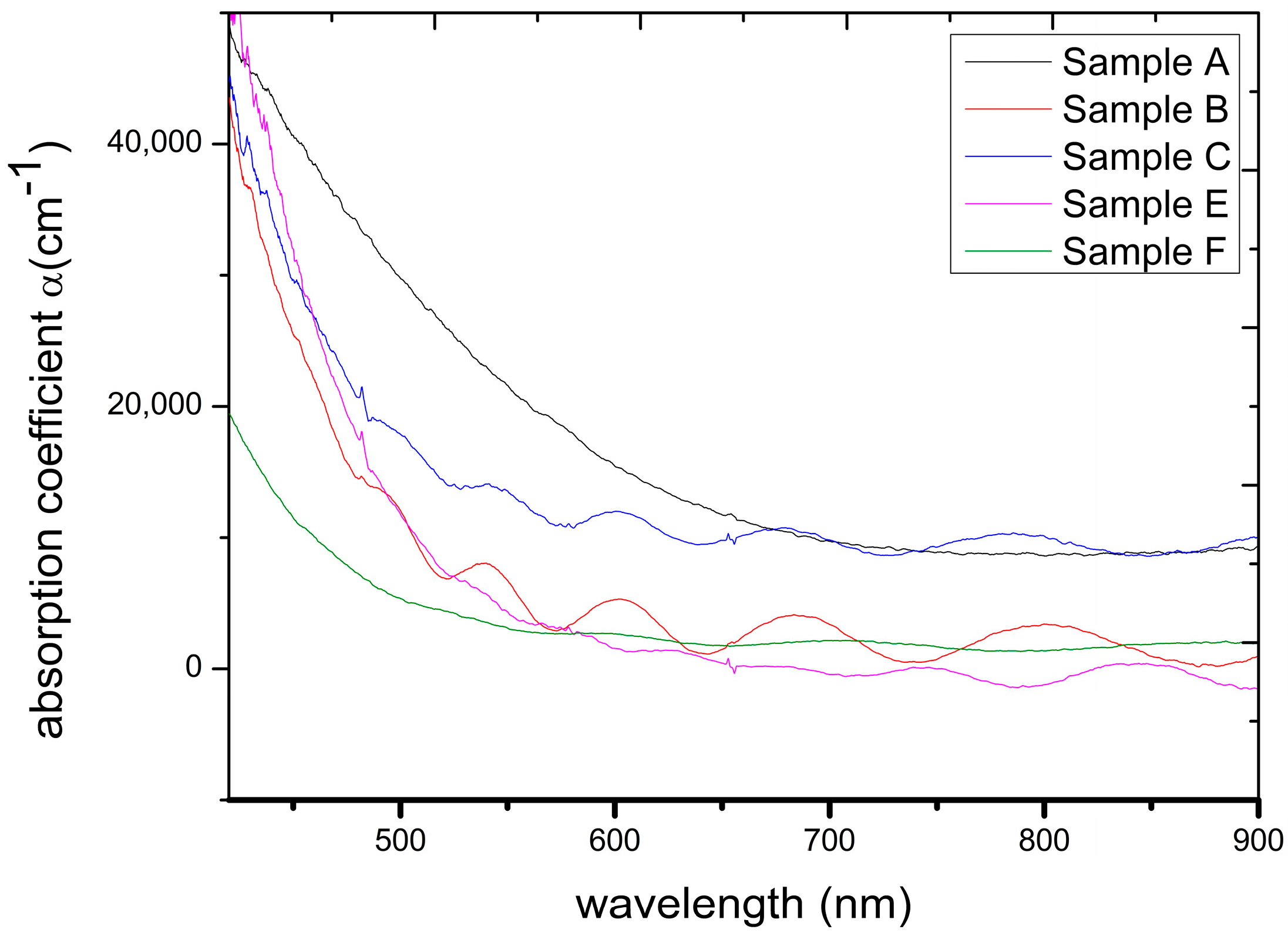
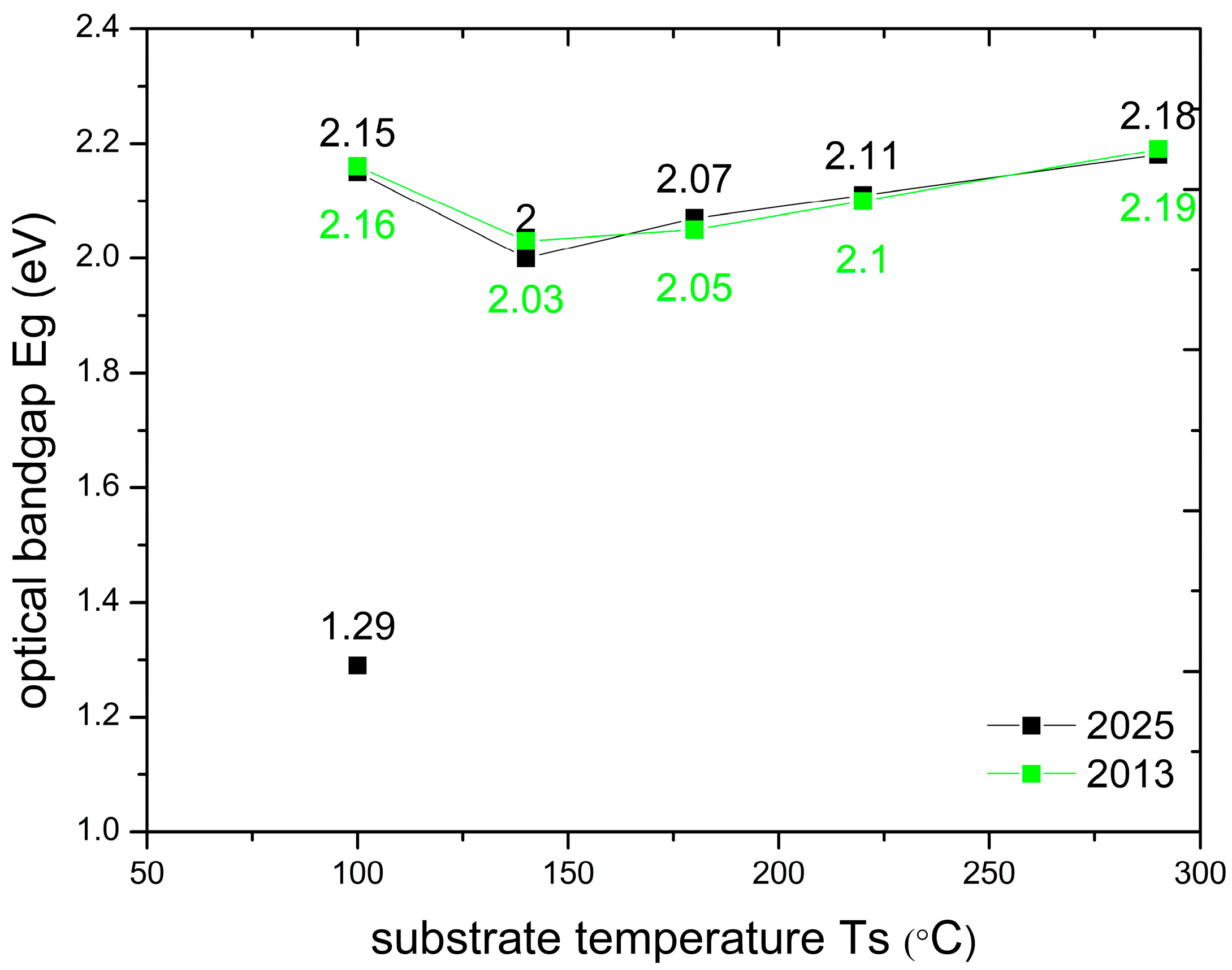
Figure 1. Absorbance coefficient versus wavelength.
Electronicmat 06 00008 g001
Figure 2. α h v versus photon energy (hν) and calculation of the optical band gap energies via Mott and Davis method. The black dotted lines indicate the Egs, extracted from their points of intersection with the X-axis.
Electronicmat 06 00008 g002
Figure 3. Optical band gap energy versus substrate temperature.
Electronicmat 06 00008 g003
Figure 4. Refractive index versus substrate temperature.
Electronicmat 06 00008 g004
Table 1. Slope B of a-SiC:H thin films deposited in different substrate temperatures and under hydrogen flow.
SampleSubstrate
Temperature Ts
Optical Bandgap EgSlope BRefractive
Index n
Hydrogen Flow
A 100   ° C 1.29224.343.9170 sccm
B 100   ° C 2.15450.932.62320 sccm
C 140   ° C 2353.633.14220 sccm
D 180   ° C 2.073992.8120 sccm
Ε 220   ° C 2.11460.322.49320 sccm
F 290   ° C 2.18308.381.88720 sccm
Disclaimer/Publisher’s Note: The statements, opinions and data contained in all publications are solely those of the individual author(s) and contributor(s) and not of MDPI and/or the editor(s). MDPI and/or the editor(s) disclaim responsibility for any injury to people or property resulting from any ideas, methods, instructions or products referred to in the content.

