Article

Modeling of Magnetoconductivity (MC) Behavior in Dilute p-Si/SiGe/Si

by
Hamza Mabchour
1,
Yassine Essakali
2,
Mounir El Hassan
1,
Samir Elouaham
3,*,
Boujemaa Nassiri
4,
Said Dlimi
2,* and
Abdelhamid El Kaaouachi
5,*
1
Laboratory of Energetic Engineering and Materials, Faculty of Sciences, Ibn Tofail University, Kenitra 14000, Morocco
2
Laboratory of Sciences and Technologies of Information and Communication, Department of Physics, Faculty of Sciences, Chouaib Doukkali University, El Jadida 24000, Morocco
3
Information Systems and Technology Engineering Laboratory (LISTI), National School of Applied Sciences, Ibn Zohr University, Agadir 80000, Morocco
4
LIDRA Inter Disciplinary Applied Research Laboratory, International University of Agadir—Universiapolis, Agadir 80000, Morocco
5
Physics Department, Faculty of Sciences, Ibn Zohr University, Agadir 80000, Morocco
*
Authors to whom correspondence should be addressed.
Electron. Mater. 2025, 6(2), 5; https://doi.org/10.3390/electronicmat6020005
Submission received: 20 March 2025 / Revised: 22 April 2025 / Accepted: 28 April 2025 / Published: 29 April 2025

Abstract

:
In this study, we investigate the magnetoconductivity behavior in a 2D p-Si/SiGe/Si system. To achieve this, we develop a theoretical model that incorporates three key contributions, the weak localization effect, electron–electron interaction effects, and the Zeeman effect, which is considered only in the presence of a magnetic field. We then compare our theoretical predictions with experimental magnetoconductivity data, analyzing both the consistencies and discrepancies between the model and the measurements. Through this comparison, we aim to provide a deeper physical understanding of the factors influencing magnetoconductivity in this system.

1. Introduction

The study of magnetoconductivity (MC) in low-dimensional semiconductor systems has attracted significant attention due to its fundamental importance in condensed matter physics and its potential applications in spintronics and quantum devices [1,2,3,4,5]. Among these systems, dilute p-type Si/SiGe/Si heterostructures offer a unique platform for investigating quantum transport phenomena under the influence of an external magnetic field.
Previously we analyzed the electrical conductivity on both sides of the Metal–Insulator Transition (MIT) and the behavior of positive and negative magnetoconductivity in different materials with semiconducting behavior in 2D and 3D. We used several very complex theoretical models to explain the observed behaviors [6,7,8,9]. The choice of these models taken into consideration is determined according to whether the investigations were carried out on the insulating side or the metallic sides of the MIT [10,11,12]. Indeed, on the insulating side of the MIT, and in order to explain the negative behavior of the magnetoresistivity, we used three theoretical models to model the experimental results of the negative magnetoresistivity. The magnetic moment model [13] uses the notion of magnetic moments localized on the impurity centers. The conduction electrons are diffused by these magnetic moments. The model of Nguyen et al. [14] considers the hopping of an electron between two sites separated by an optimal hopping distance Rhop. The hopping probability between these two sites is determined by the interference between the multiple possible connection paths inside a coherence volume. This volume, in which the two scattered electrons will keep their phase coherence, is an ellipsoid of length Rhop and width R h o p 1 / 2 ξ , where ξ denotes the localization length. The application of magnetic field B changes the hopping probability by introducing a different phase factor for each scattering path. When the magnetic flux Φ through the surface R h o p 1 / 2 ξ 3 / 2 reaches a flux quantum ϕ 0 = h / 2 π e , the amplitude of the negative magnetoresistivity becomes maximal.
The Shirmacher model [15], which involves quantum interferences. Starting from the principle that in a Variable Rang Hopping (VRH) conduction regime, very few intermediate sites can take place in the hopping interval defined by Rhop, Shirmacher calculates the probability of thermally assisted hopping during the process involving a single intermediate site located below the Fermi level. To do this, he uses the formalism developed by Holstein [16] where the electron–phonon interactions are treated in the deformation potential approximation and the electronic eigenstates are calculated by the re-normalized perturbation theory. The best results of our modeling were obtained with the magnetic moment model. On the metallic side of MIT, in our magnetoresistivity modeling, we used the theories dealing with electron–electron interaction effects, the weak localization effect, and the Zeeman effect in the presence of a magnetic field.
In this work and our investigation, we reuse the experimental measurements of the 2D p-Si/SiGe/Si sample with a carrier density of p = 8.2 × 1010 cm−2 obtained by I. L Drichko et al. [17,18]. These measurements were carried out at temperatures T ranging from 0.3 K to 1.6 K with magnetic field B between 0 and 7.2 T. Hole mobility is equal to μ = 1 × 10 4   c m 2 / V s at liquid helium temperatures. The 2D system Si/SiGe/Si/(001)Si was grown on a Si (001) substrate by the solid source molecular-beam epitaxy. It consisted of the 300 nm Si buffer layer followed by 30 nm Si0.92 Ge0.08 layer. In Figure 1, we present experimental measurements [19] of magnetoconductivity (MC) against magnetic field B. We notice that this MC is negative for the entire interval of magnetic fields [0–7.2 T]. The zero conductivity values at T = 0 K are obtained by linear regression of the curves σ ( B , T ) against temperature T for different magnetic fields B (Figure 2). This negativity increases when the temperature increases. This interval of magnetic field corresponds to the metallic side of MIT [20,21,22,23]. In this work, we focus on modeling the MC behavior in a 2D p-Si/SiGe/Si system, considering the combined effects of weak localization, electron–electron interactions, and the Zeeman effect. While weak localization contributes positively to MC, electron–electron interactions and the Zeeman effect introduce negative contributions, influencing the overall conductivity behavior. By comparing our theoretical model with available experimental data, we aim to provide a comprehensive understanding of the underlying physical mechanisms governing MC in this system. Additionally, we discuss possible extensions of the model, considering factors such as material layer configurations, which could further refine the description of MC in 2D semiconductor heterostructures.

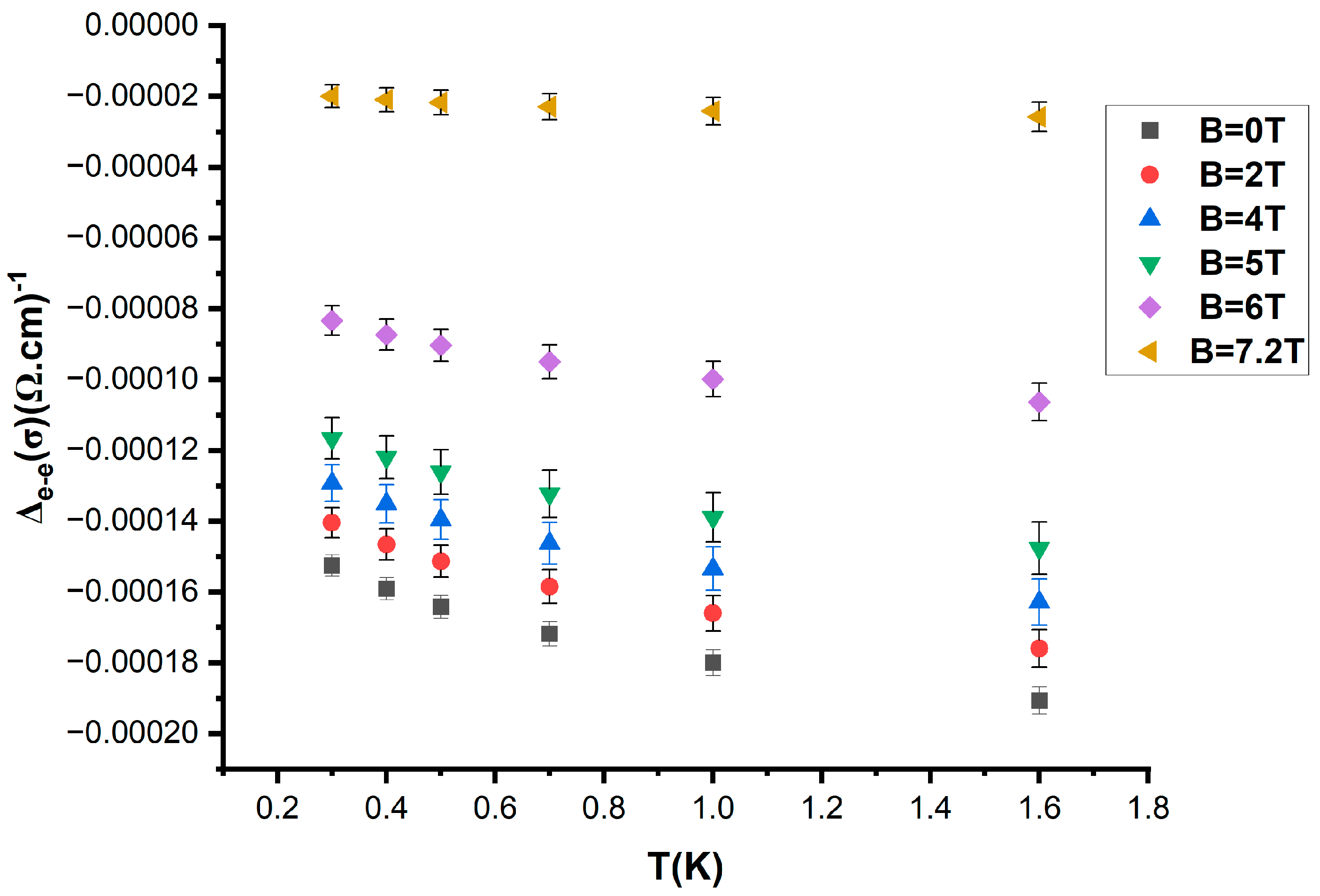
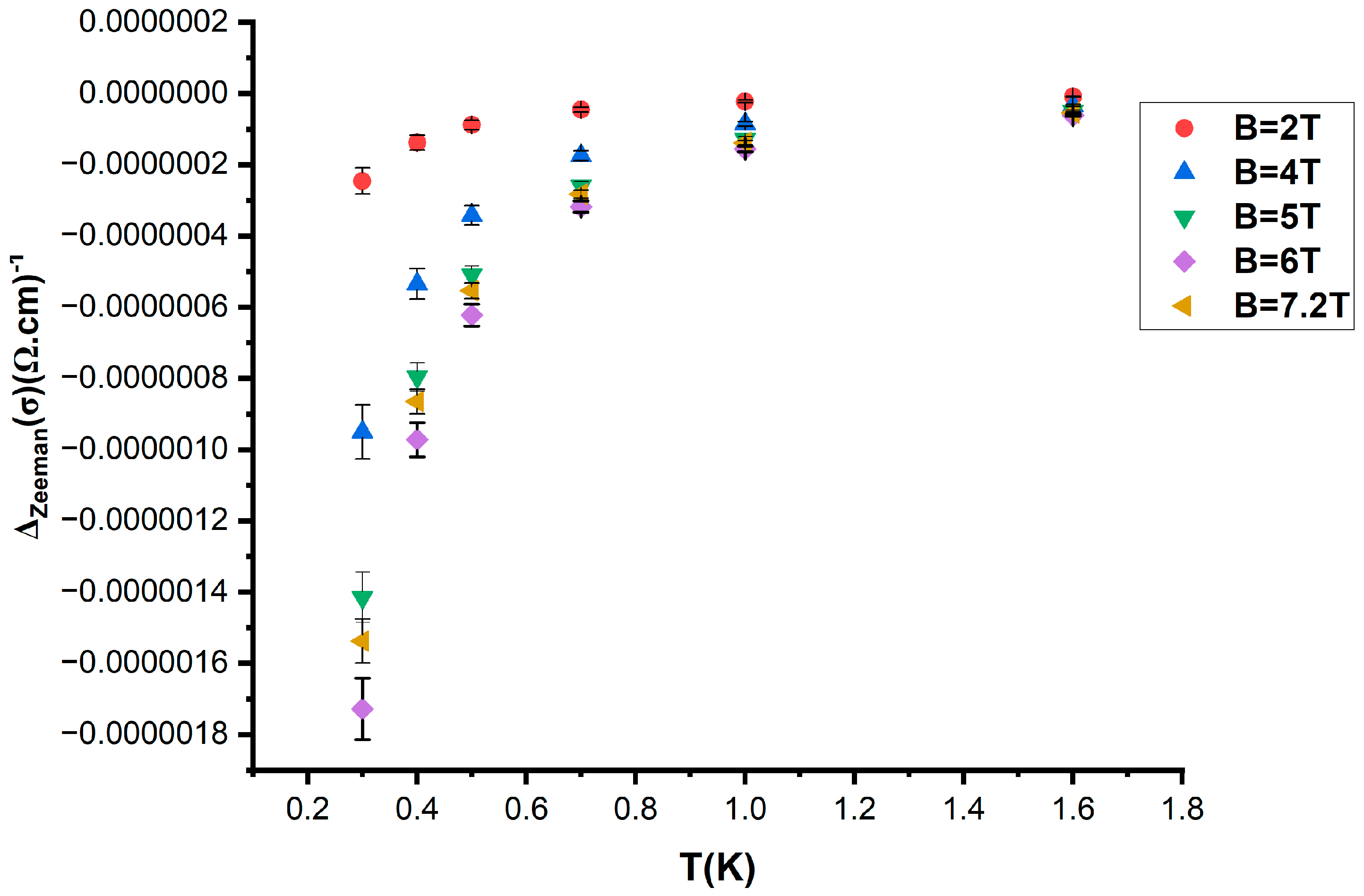
2. Construction of a Theoretical Model for MC

We will build a theoretical model to explain this negative behavior of the MC on the metal side of the MIT in the sample 2D p-Si/SiGe/Si. So, we will take into account the effect of weak localization, the effects of electron–electron interactions and the Zeeman effect in 2D systems. The expression of MC correction can be defined as:
Δ σ ( B , T ) = Δ ( σ W L ) + Δ ( σ e e ) + Δ ( σ Z e e m a n )
where Δ ( σ W L ), Δ ( σ e e ), and Δ ( σ Z e e m a n ) are, respectively, the contributions of the weak localization effect, electron–electron interactions effects, and Zeeman effect to the expression of MC.
Δ ( σ W L ) is given by [20,24]
Δ   ( σ W L ) = α p e 2 π ћ ln   ( k B T τ ћ ) ,
where α = 1 for the diffusion of impurities (−1/2 for spin–orbit diffusion and 0 for spin diffusion), p is the exponent in the temperature dependence of the inelastic diffusion time τ T p , and p is close to 1 [25].
Δ ( σ e e ) is given by [24]
Δ   ( σ e e ) = e 2 π ћ ( 1 3 F 0 σ 4 )   ln   ( k B T τ ћ ) ,
where F 0 σ is the Fermi liquid parameter.
The Zeeman effect refers to the splitting of an energy level into multiple sub-levels with distinct energies due to the influence of an external magnetic field B. The term Δ ( σ Z e e m a n ) is given by [26,27,28]
Δ   ( σ Z e e m a n ) = F 0 σ 2 e 2 π 2 ћ g ( h ) ,
where h = B u B g * k B T with g* being the g-factor of spins. The function g(h) is known:
g(h) = 0.084 h2 for h << 1 and g(h) = ln(h/1.3) for h >> 1 [28].
The complete theoretical model is expressed as
Δ σ ( B , T ) = Δ ( σ W L )   +   Δ ( σ e e )   +   Δ   ( σ Z e e m a n ) = α p e 2 π ћ ln   ( k B T τ ћ ) + e 2 π ћ ( 1 3 F 0 σ 4 )   ln   ( k B T τ ћ ) F 0 σ 2 e 2 π 2 ћ g ( h ) ,

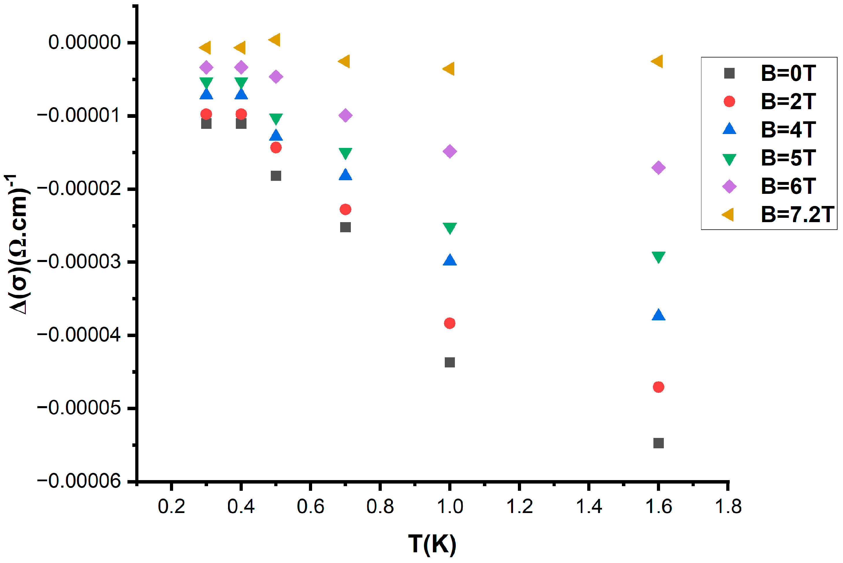
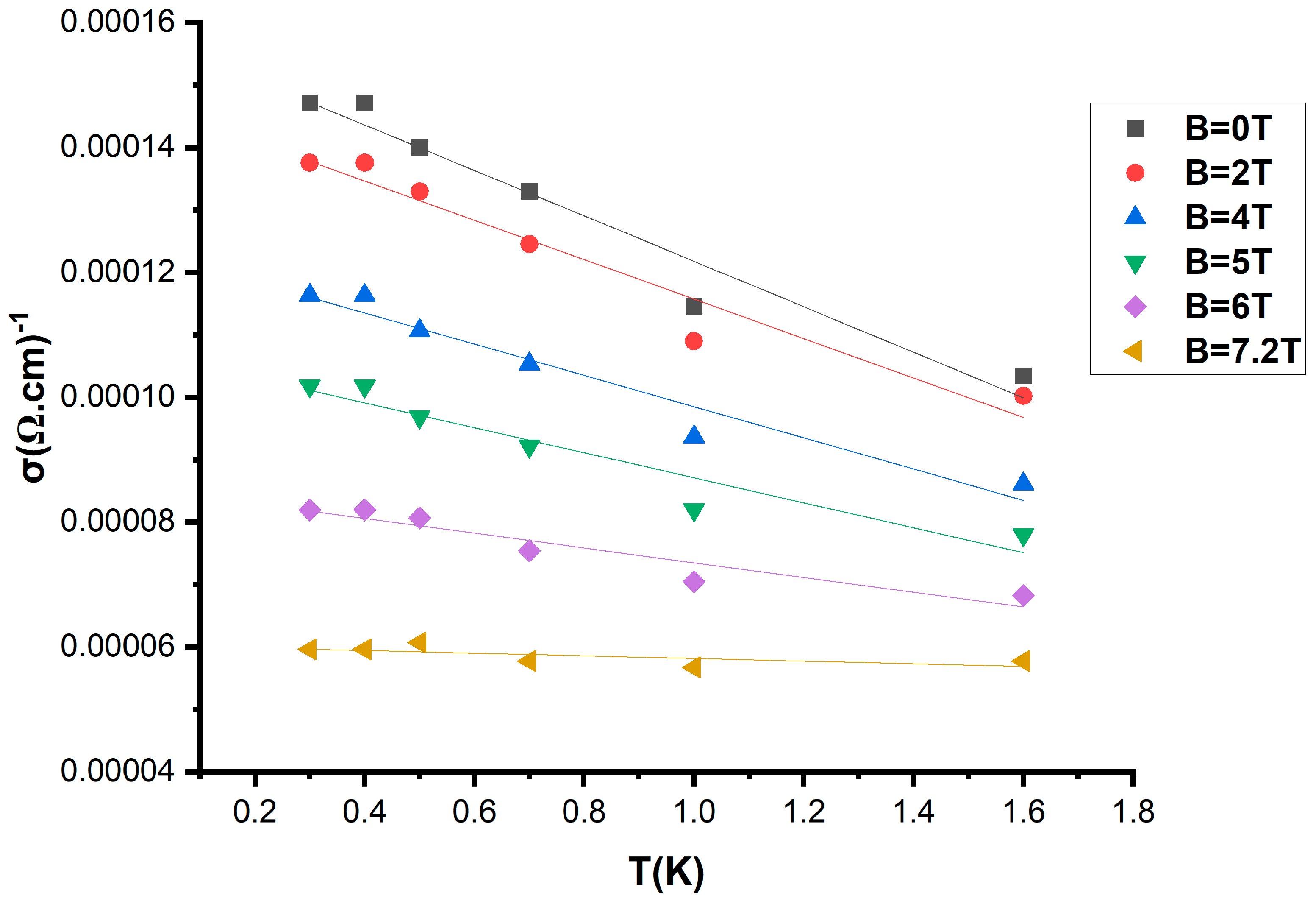
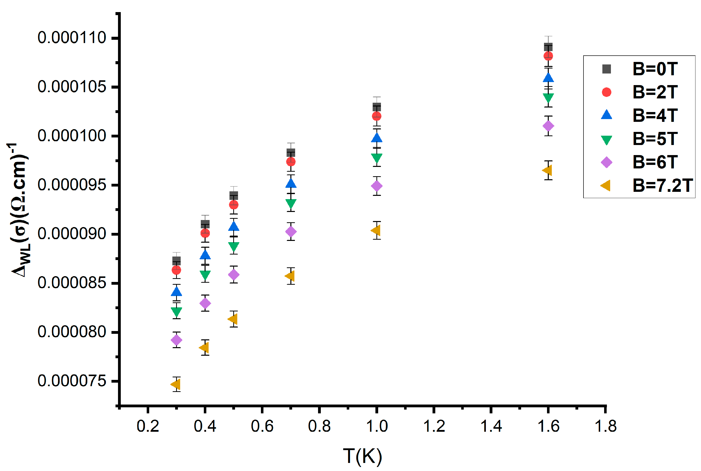
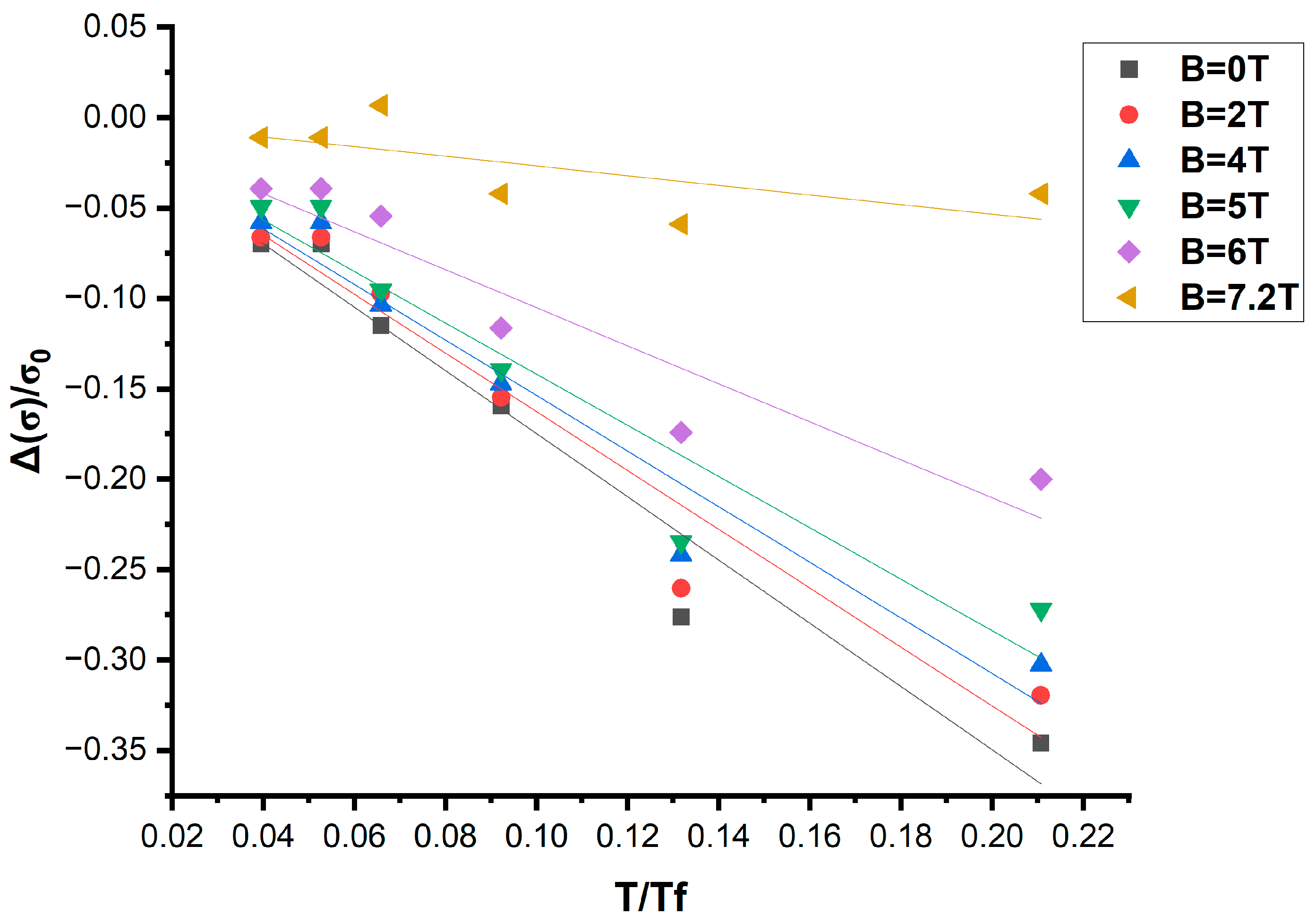
3. Results and Discussion

Expression (2) of Δ ( σ W L ) is always positive for this 2D p-Si/SiGe/Si sample because k B T τ ћ 1 . In Figure 3, we present Δ ( σ W L ) versus T for different values of magnetic field B. It is clear that this contribution of weak localization effect to MC is positive over the entire temperature range. This positivity increases when magnetic field B tends towards zero.
Concerning the contribution to MC due to electron–electron interactions effect given by Equation (3), the term ln ( k B T τ ћ ) is always positive ( k B T τ ћ 1 ) and the sign of this contribution depends on the sign of the term (1 − 3 F 0 σ 4 ). We need to determine the values of the parameter F 0 σ for each value of B. We use the following expression [29]:
Δ ( σ ) σ 0 B , T = 0 = ( 1 3 F 0 σ 4 ) T T F ,
where TF is the Fermi temperature given by T F = E F k B = ћ 2 k F 2 2 k B 2 m * ( k F = 2 π n p ). k F is the Fermi vector. Figure 4 shows Δ ( σ ) σ 0 B , T = 0 versus T T F , for different values of B. The slopes a(B) of these curves allow us to determine the values of the parameter F 0 σ . In fact, the slopes σ(B) = (1 − 3 F 0 σ 4 ). This allows us to extract the values of the parameter F 0 σ for each value of the magnetic field. F 0 σ varies between 1.68975 for B = 7.2 T and 3.66316 for B = 0 T. F 0 σ increases when magnetic field decreases. Fermi liquid properties are observed at low temperatures in almost all systems. A Fermi liquid is a quantum state of matter, observed at low temperatures for most 2D and 3D crystalline solids and in liquid helium-3. It is characterized macroscopically by universal thermodynamic, magnetic, and transport properties (e.g., electrical conductivity) corresponding to those of a gas of quasi-particles having the same spin-1/2, the same charge, and the same volume under the Fermi surface as electrons (or helium-3 atoms), but a renormalized mass called “effective mass”, as well as residual interactions. In solids, the effective mass reflects the fact that interactions between electrons or with atoms in the crystal (band structure and electron–phonon interaction) modify the mobility of conduction electrons. These values give us a term (1 − 3 F 0 σ 4 ) < 0 for all magnetic fields B. So Δ ( σ e e ) < 0. In previous work, we obtained the same result in the 2D-layerd sample WS2 [30].
In Figure 5, we present Δ ( σ e e ) versus T for different values of magnetic field B using Equation (2). This contribution is negative. It becomes smaller as the magnetic field tends towards zero. This can be explained by the fact that as B increases, the electrons are more agitated and the interactions between electrons become more frequent.
Regarding the contribution to MC of Zeeman effects (Δ ( σ Z e e m a n ) , Figure 6) expressed by Equation (4), it is also negative over the entire magnetic field range [2–7.2 T].
This negativity is all the more accentuated as the magnetic field increases. This is due to the fact that the degeneracy of the spins is more important when B increases. We also note that the theoretical values of Δ ( σ Z e e m a n ) come very close when the temperature T tends towards the value 1.6 K.
The experimental MC (Figure 1) is negative over the entire magnetic field range [0–7.2 T]. Theoretical calculations of the contributions to the MC due to the electron–electron interaction effects and the Zeeman effect are negative, while the theoretical contribution of weak localization is positive. We can deduce that the electron–electron interaction effects added to the Zeeman effect (negative contributions) are more predominant than the weak localization effects (positive contribution) over the entire magnetic field range [0–7.2 T]. That said, we observe that this experimental MC (Figure 1) tends towards zero for the value of the magnetic field B = 7.2 T. Recently, we observed a change in the sign of the MC in the 2D-layered sample WS2 [30]. Indeed, we noted that the MC is positive for high temperatures (100 and 200 K) on all the magnetic field ranging 0–15 T. This MC becomes negative starting from the temperature T = 60 K. In our case, this would suggest a change in the sign of the experimental MC for BC > B > 7.2 T. Where BC is the critical field separating the two metallic and insulating sides of the Metal–Insulator Transition (MIT) [31]. An increase in temperature could also contribute to this change in sign.
Recently, R. Basnet et al. [32] studied magnetoresistivity on Sn-rich Sn1−xGex thin films enabled by the CdTe buffer layer, and they observed a positive magnetoresistivity (PMR) which translates into a negative magnetoconductivity (NMC) whose behavior is similar to our results. Indeed, they obtain a PMR which increases when the magnetic field increases for all temperature values. That said, this PMR takes on more magnitude when the temperature increases and changes curvature from T = 100 K. We used very low temperatures [0.3–1.6 K] compared to those used by Bastnet et al. [32], which leads us to think that it would be very interesting to carry out magnetoconductivity measurements at temperatures close to the interval [0.3–1.6 K] and test our theoretical model to model this MC. They successfully grew thin films of α-Sn and α-Sn0.975Ge0.025 on an InSb substrate using a resistive CdTe epitaxial buffer layer to reduce the contribution of the InSb substrate to electronic transport.
Other authors have obtained a NMC on Sn4Au single crystal [33], its negativity increasing with decreasing temperature. This behavior has been explained using another approach based on the Hikami–Larkin–Nagaoka formalism, which assumes the presence of a weak antilocalization (WAL) effect in Sn4Au. In the same sense, K. Kapul et al. [34] also observed a very high positive MR at T = 2 K in magnetic Weyl semimetal Co3Sn2S2. This MR decreases when the temperature increases and becomes negative when the temperature T is higher than 70 K. Authors fitted low-field magnetoconductivity data up to ±1 T (Tesla) also using the Hikami Larkin Nagaoka model, which shows the presence of a weak antilocalization (WAL) effect in the Co3Sn2S2 crystal synthesized at low temperatures below 30 K. It would be very productive to try to model the experimental results used in our paper using this formalism. This would allow us to compare the effects of weak localization with those of weak antilocalization.

4. Conclusions

In this work, we analyzed the experimentally observed negative magnetoconductivity (MC) in p-Si/SiGe/Si, aiming to provide a comprehensive physical explanation for this behavior. To achieve this, we developed a theoretical model incorporating weak localization effects, electron–electron interaction effects, and the Zeeman effect, the latter being considered only in the presence of a magnetic field. Our analysis reveals that while weak localization effects contribute positively to MC, both electron–electron interaction effects and the Zeeman effect contribute negatively. The significant increase in negative magnetoconductivity observed in a parallel magnetic field is most likely attributed to the interaction between the in-plane magnetic field and the orbital motion of charge carriers within the quasi-two-dimensional (quasi-2D) layer of finite thickness. This phenomenon can be qualitatively explained within the framework of existing theoretical models [35,36]. In contrast, the lack of a strong influence of the in-plane magnetic field on conductivity, as reported in Refs. [37,38,39], may be due to the relatively high carrier density in the system investigated in that study. This interpretation aligns with these experimental findings, particularly for the sample with a carrier density of p = 8.2 × 1010 cm−2, where a similar trend is observed. Our findings indicate that, under the experimental conditions of this p-Si/SiGe/Si sample, the impact of weak localization is less significant than the combined influence of electron–electron interactions and the Zeeman effect, leading to an overall negative MC. Furthermore, additional factors could be considered to refine the MC modeling, such as the effect of the material’s layer structure [40,41]. For instance, in graphene and other two-dimensional layered materials, local MC can be understood by considering differential transport parameters, including carrier mobility variations across different layers under an external magnetic field. Meanwhile, non-local MC has been attributed to the Ettingshausen–Nernst effect induced by magnetic fields. Incorporating such considerations could further enhance the accuracy of MC modeling in complex multilayered systems.

Author Contributions

Conceptualization, H.M. and A.E.K.; methodology, A.E.K.; software, H.M. and M.E.H.; validation, Y.E., S.D. and A.E.K.; formal analysis, S.E.; investigation, Y.E.; writing—original draft preparation, A.E.K., Y.E and H.M.; writing—review and editing, S.D.; visualization, B.N.; supervision, A.E.K. All authors have read and agreed to the published version of the manuscript.

Funding

This research received no external funding.

Data Availability Statement

The data supporting the findings of this study are available from the corresponding author upon reasonable request.

Acknowledgments

We extend our gratitude to the Publications Marketing Coordinator of the American Physical Society (APS) for granting permission to reuse the experimental data.

Conflicts of Interest

The authors declare no conflicts of interest regarding the publication of this paper. The authors have no relevant financial or non-financial interests to disclose.

References

  1. Babar, Z.U.D.; Raza, A.; Cassinese, A.; Iannotti, V. Two Dimensional Heterostructures for Optoelectronics: Current Status and Future Perspective. Molecules 2023, 28, 2275. [Google Scholar] [CrossRef] [PubMed]
  2. Yoon, M. The Extraction of the Density of States of Atomic-Layer-Deposited ZnO Transistors by Analyzing Gate-Dependent Field-Effect Mobility. Electron. Mater. 2024, 5, 239–248. [Google Scholar] [CrossRef]
  3. Hasan, M.N.; Li, C.; Lai, J.; Seo, J.-H. Theoretical Prediction of Heterogeneous Integration of Dissimilar Semiconductor with Various Ultra-Thin Oxides and 2D Materials. Electron. Mater. 2021, 2, 495–503. [Google Scholar] [CrossRef]
  4. Chiang, T.-K. A Unified Semiconductor-Device-Physics-Based Ballistic Model for the Threshold Voltage of Modern Multiple-Gate Metal-Oxide-Semiconductor Field-Effect-Transistors. Electron. Mater. 2024, 5, 321–330. [Google Scholar] [CrossRef]
  5. Darwish, M.; Pohl, L. Insulator Metal Transition-Based Selector in Crossbar Memory Arrays. Electron. Mater. 2024, 5, 17–29. [Google Scholar] [CrossRef]
  6. Dlimi, S.; Limouny, L.; El kaaouachi, A. Crossover between ballistic and diffusive regime in 2D SiGe quantum well. Appl. Surf. Sci. Adv. 2021, 3, 100045. [Google Scholar] [CrossRef]
  7. Limouny, L.; El kaaouachi, A.; Abdia, R.; Narjis, A.; Biskupski, G.; Hemine, J.; Sybous, A.; Dlimi, S. Study of electrical resistivity in 2D Si-MOSFETS at very low temperature. AIP Conf. Proc. 2012, 1435, 385. [Google Scholar]
  8. Dlimi, S.; El kaaouachi, A.; Narjis, A.; Limouny, L.; Sybous, A.; Errai, M.; Daoudi, E. Evidence for the correlated hopping mechanism in p-GaAs near the 2D MIT AT B=0T. J. Optoelectron. Adv. Mater. 2013, 15, 1222. [Google Scholar]
  9. Elmourabit, F.; Dlimi, S.; El Moutaouakil, A.; Ouissaaden, F.I.; Khoukh, A.; Limouny, L.; Elkhatat, H.; El kaaouachi, A. Nature of the Metal Insulator Transition in High-Mobility 2D_Si-MOSFETs. Nanomaterials 2023, 13, 2047. [Google Scholar] [CrossRef]
  10. Huth, M.; Klingenberger, D.; Grimm, C.; Porrati, F.; Sachser, R. Conductance regimes of W-based granular metals prepared by electron beam induced deposition. New J. Phys. 2009, 11, 033032. [Google Scholar] [CrossRef]
  11. Lenko, D.; Schlögl, S.; Bichler, S.; Lemesch, G.; Ramsauer, F.; Ladstätter, W.; Rosc, J.; Kern, W. New approaches towards the investigation on defects and failure mechanisms of insulating composites used in high voltage applications. Compos. Part B Eng. 2014, 58, 83–90. [Google Scholar] [CrossRef]
  12. Qu, L.; Vörös, M.; Zimanyi, G.T. Metal-Insulator Transition in Nanoparticle Solids: Insights from Kinetic Monte Carlo Simulations. Sci. Rep. 2017, 7, 7071. [Google Scholar] [CrossRef] [PubMed]
  13. Toyozwa, Y. Theory of Localized Spins and Negative Magnetoresistance in the Metallic Impurity Conduction. J. Phys. Soc. Jap. 1962, 14, 986. [Google Scholar] [CrossRef]
  14. Nguyen, V.L.; Spivak, B.Z.; Shklovskii, B.I. Tunnel hopping in disordered systems. Sov. Phys. JETP 1985, 62, 1021. [Google Scholar]
  15. Schirmacher, W. Quantum-interference magnetoconductivity in the variable-range-hopping regime. Phys. Rev. B 1990, 41, 2461. [Google Scholar] [CrossRef]
  16. Holstein, T. Hall Effect in Impurity Conduction. Phys. Rev. B 1961, 108, 222. [Google Scholar] [CrossRef]
  17. Drichko, L.; Smirnov, I.Y.; Suslov, A.V.; Mironov, O.A.; Leadley, D.R. Large magnetoresistance of a dilute p-Si/SiGe/Si quantum well in a parallel magnetic field. Phys. Rev. B 2009, 79, 205310. [Google Scholar] [CrossRef]
  18. Drichko, I.L.; Dyakonov, A.M.; Smirnov, I.Y.; Suslov, A.V.; Galperin, Y.M.; Vinokur, V.; Myronov, M.; Mironov, O.A.; Leadley, D.R. Magnetotransport in low-density p-Si/Si Ge heterostructures: From metal through hopping insulator to Wigner glass. Phys. Rev. B 2008, 77, 085327. [Google Scholar] [CrossRef]
  19. Altshuler, B.L.; Aronov, A.; Khmelnitski, D.E. Effects of electron-electron collisions with small energy transfers on quantum localization. J. Phys. C Solid. State Phys. 1982, 15, 7367. [Google Scholar] [CrossRef]
  20. Altshuler, B.L.; Aronov, A.; Khmelnitski, D.E. Suppression of localization effects by the high frequency field and the nyquist noise. Solid. State. Commun. 1981, 39, 619. [Google Scholar] [CrossRef]
  21. Shashkin, A.A.; Dolgopolov, V.T.; Huang, S.-H.; Liu, C.W.; Zhu, A.Y.X.; Kravchenko, S.V. Metallic state in a strongly interacting spinless two-valley electron system in two dimensions. Phys. Rev. B 2020, 101, 045302. [Google Scholar]
  22. Shlimak, I.; Butenko, A.; Golosov, D.I.; Friedland, K.-J.; Kravchenko, S.V. Influence of spin polarization on resistivity of a two-dimensional electron gas in Si MOSFET at metallic densities. Europhys. Lett. 2012, 97, 37002. [Google Scholar] [CrossRef]
  23. Kopelevich, Y.; Pantoja, J.C.M.; da Silva, R.R.; Moehlecke, S. Universal magnetic-field-driven metal-insulator-metal transformations in graphite and bismuth. Phys. Rev. B 2006, 73, 165128. [Google Scholar] [CrossRef]
  24. Senz, V.; Ihn, T.; Heinzel, T.; Ensslin, K.; Dehlinger, G.; Grùtzmacher, D.; Gennser, U. Analysis of the Metallic Phase of Two-Dimensional Holes in SiGe in Terms of Temperature Dependent Screening. Phys. Rev. Lett. 2000, 85, 4357. [Google Scholar] [CrossRef] [PubMed]
  25. Lei, Z.; Cheah, E.; Rubi, K.; Bal, M.E.; Adam, C.; Schott, R.; Zeitler, U.; Wegscheider, W.; Ihn, T.; Ensslin, K. High-quality two-dimensional electron gas in undoped InSb quantum wells. Phys. Rev. Res. 2022, 4, 013039. [Google Scholar] [CrossRef]
  26. Kawabata, J. Theory of negative magnetoresistance in three-dimensional systems. Solid. State. Commun. 1980, 34, 431. [Google Scholar] [CrossRef]
  27. Dlimi, S.; El Kaaouachi, A.; Limouny, L. Magnetoconductivity in a Disordered and Interacting 2D p-SiGe Quantum Well. J. Korean. Phys. Soc. 2020, 77, 1218. [Google Scholar] [CrossRef]
  28. Lee, P.A.; Ramakrishnan, T.V. Magnetoresistance of weakly disordered electrons. Phys. Rev. B 1982, 26, 4009. [Google Scholar] [CrossRef]
  29. Altshuler, B.L.; Aronov, A.; Larkin, A.I.; Khmelnitski, D.E. Negative magnetoresistance in semiconductors in the hopping conduction region. Sov. Phys. JETP 1981, 54, 411. [Google Scholar]
  30. Mounir, E.; Mabchour, H.; Hammou, B.A.; El Oujdi, A.; Dlimi, S.; El kaaouachi, A. Magnetoconductivity behaviour due to electron–electron interactions, weak localization and Zeeman effects in 2-D-layered WS2. Bull. Mater. Sci. 2024, 47, 161. [Google Scholar] [CrossRef]
  31. Sarma, S.D.; Hwang, E.H. Parallel Magnetic Field Induced Giant Magnetoresistance in Low Density Quasi-Two-Dimensional Layers. Phys. Rev. Lett. 2000, 84, 5596. [Google Scholar]
  32. Basnet, R.; Upreti, D.; McCarthy, T.T.; Ju, Z.; McMinn, A.M.; Sharma, M.M.; Zhang, Y.-H.; Hu, J. Magneto-transport study on Sn-rich Sn1−xGex thin films enabled by CdTe buffer layer. J. Vac. Sci. Technol. B 2024, 42, 042210. [Google Scholar] [CrossRef]
  33. Sharma, M.M.; Rani, P.; Awana, V.P.S. Probing the topological surface states in superconducting Sn4Au single crystal: A magneto transport study. J. Phys. Condens. Matter. 2022, 34, 415701. [Google Scholar] [CrossRef] [PubMed]
  34. Kumar, K.; Sharma, M.M.; Awana, V.P.S. Weak antilocalization and ferromagnetism in magnetic Weyl semimetal Co3Sn2S2. Appl. Phys. Lett. 2023, 133, 023901. [Google Scholar] [CrossRef]
  35. Liu, H.-L.; Luo, Z.-Y.; Guo, J.-J.; Wang, X.-G.; Nie, Y.-Z.; Xia, Q.-L.; Guo, G.-H. Magnetoresistance and magnetic field-induced phase transition in two-dimensional antiferromagnet Fe1/3NbS2. AIP Adv. 2024, 14, 055220. [Google Scholar] [CrossRef]
  36. Papp, G.; Peeters, F.M. Giant magnetoresistance in a two-dimensional electron gas modulated by magnetic barriers. J. Phys. Condens. Matter 2004, 16, 8275. [Google Scholar] [CrossRef]
  37. Dorozhkin, S.I.; Emeleus, C.J.; Whall, T.E.; Landwehr, G. Tuning of the quantum-Hall-effect-state–insulator transition by tilting of magnetic field. Phys. Rev. B 1995, 52, R11638. [Google Scholar] [CrossRef]
  38. Yoshimi, R.; Tsukazaki, A.; Kozuka, Y.; Falson, J.; Takahashi, K.; Checkelsky, J.; Nagaosa, N.; Kawasaki, M.; Tokura, Y. Quantum Hall effect on top and bottom surface states of topological insulator (Bi1−xSbx)2Te3 films. Nat. Commun. 2015, 6, 6627. [Google Scholar] [CrossRef]
  39. Lu, T.M.; Tracy, L.A.; Laroche, D.; Huang, S.-H.; Chuang, Y.; Su, Y.-H.; Li, J.-Y.; Liu, C.W. Density-controlled quantum Hall ferromagnetic transition in a two-dimensional hole system. Sci. Rep. 2017, 7, 2468. [Google Scholar] [CrossRef]
  40. Abrisokov, A. Quantum linear magnetoresistance. Europhys. Lett. 2000, 49, 789. [Google Scholar]
  41. Gopinadhan, K.; Shin, Y.J.; Jalil, R.; Venkatesan, T.; Geim, A.; Neto, A.H.C.; Yang, H. Extremely large magnetoresistance in few-layer graphene/boron–nitride heterostructures. Nat. Commun. 2015, 6, 8337. [Google Scholar] [CrossRef]
Figure 1. Magnetoconductivity (MC) versus magnetic field B.
Electronicmat 06 00005 g001
Figure 2. Electrical conductivity σ ( B , T ) versus temperature T for different values of magnetic field B.
Electronicmat 06 00005 g002
Figure 3. Δ ( σ W L ) contribution of weak localization effect to MC against temperature for different values of magnetic fields.
Electronicmat 06 00005 g003
Figure 4. Δ ( σ ) σ 0 B , T = 0 against T T F for several magnetic fields.
Electronicmat 06 00005 g004
Figure 5. Δ ( σ e e ) contribution of electron–electron interaction effects to MC against temperature for different values of magnetic fields.
Electronicmat 06 00005 g005
Figure 6. Δ ( σ Z e e m a n ) contribution of Zeeman effects to MC against temperature for different values of magnetic fields.
Electronicmat 06 00005 g006
Disclaimer/Publisher’s Note: The statements, opinions and data contained in all publications are solely those of the individual author(s) and contributor(s) and not of MDPI and/or the editor(s). MDPI and/or the editor(s) disclaim responsibility for any injury to people or property resulting from any ideas, methods, instructions or products referred to in the content.

