Article

Wear and Abrasion Resistance of Nitride Coatings on Ceramic Substrates Processed with Fast Argon Atoms

by
Sergey N. Grigoriev
,
Alexander S. Metel
*,
Marina A. Volosova
,
Enver S. Mustafaev
and
Yury A. Melnik
Department of High-Efficiency Processing Technologies, Moscow State University of Technology “STANKIN”, Vadkovskiy per. 3A, 127055 Moscow, Russia
*
Author to whom correspondence should be addressed.
Surfaces 2024, 7(3), 714-724; https://doi.org/10.3390/surfaces7030046
Submission received: 13 July 2024 / Revised: 30 August 2024 / Accepted: 2 September 2024 / Published: 4 September 2024

Abstract

:
The surfaces of ceramic products are replete with numerous defects, such as those that appear during the diamond grinding of sintered SiAlON ceramics. The defective surface layer is the reason for the low effectiveness of TiZrN coatings under abrasive and fretting wear. An obvious solution is the removal of an up to 4-µm-thick surface layer containing the defects. It was proposed in the present study to etch the layer with fast argon atoms. At the atom energy of 5 keV and a 0.5 mA/cm2 current density, the ions were converted into fast atoms and the sputtering rate for the SiAlON samples reached 20 μm/h. No defects were observed in the microstructures of coatings deposited after beam treatment for half an hour. The treatment reduced the volumetric abrasive wear by five times. The fretting wear was reduced by three to four times.

1. Introduction

To ensure the needed functional characteristics of a product, it is manufactured from expensive materials with these properties. However, in most cases, there is no need to produce the entire product from an expensive material; it is enough to modify its surface layer [1,2,3].
One can harden the surface with a pulsed electron beam without heating the bulk of the product, which leads to the distortion of its shape and size, or one can nitride the surface layer of a product up to 0.1 mm thick. It is also possible to apply to the surface a hard coating that is up to several microns thick. Often, a combined treatment is carried out, where a thin hard coating is applied to a thick nitride layer, which prevents the brittle destruction of the coating under the influence of applied forces.
Applying hard films such as TiCN, DLC, TiAlN, CrAlN and TiZrN, etc., on metal parts increases their wear resistance by about three times [4,5,6]. However, the same wear-resistant coatings on ceramic products increase the wear resistance by no more than 1.5 times. This is due to the presence on ceramic products of a defective layer that is up to 4 µm thick, which consists of grooves, voids from torn grains, micro-protrusions, scratches, etc.
For the characterization of the above defects, a “defectiveness index” Id (µm) was proposed in [7], which is determined by the formula
Id = ρ·Rt,
where ρ is the density of the defects (total area) per unit area of the ceramic sample surface (dimensionless); Rt is the maximum profile height (thickness) of the defective layer (μm) in the considered area of the ceramic sample.
Over past ten years, the use of ceramics to manufacture various products has expanded significantly [8,9]. In this regard, there is a need to study the properties of coated ceramic products and their dependence on the defectiveness of the product surface. The present study is devoted to investigation of the defectiveness influence and the ways to reduce it.

2. Materials and Methods

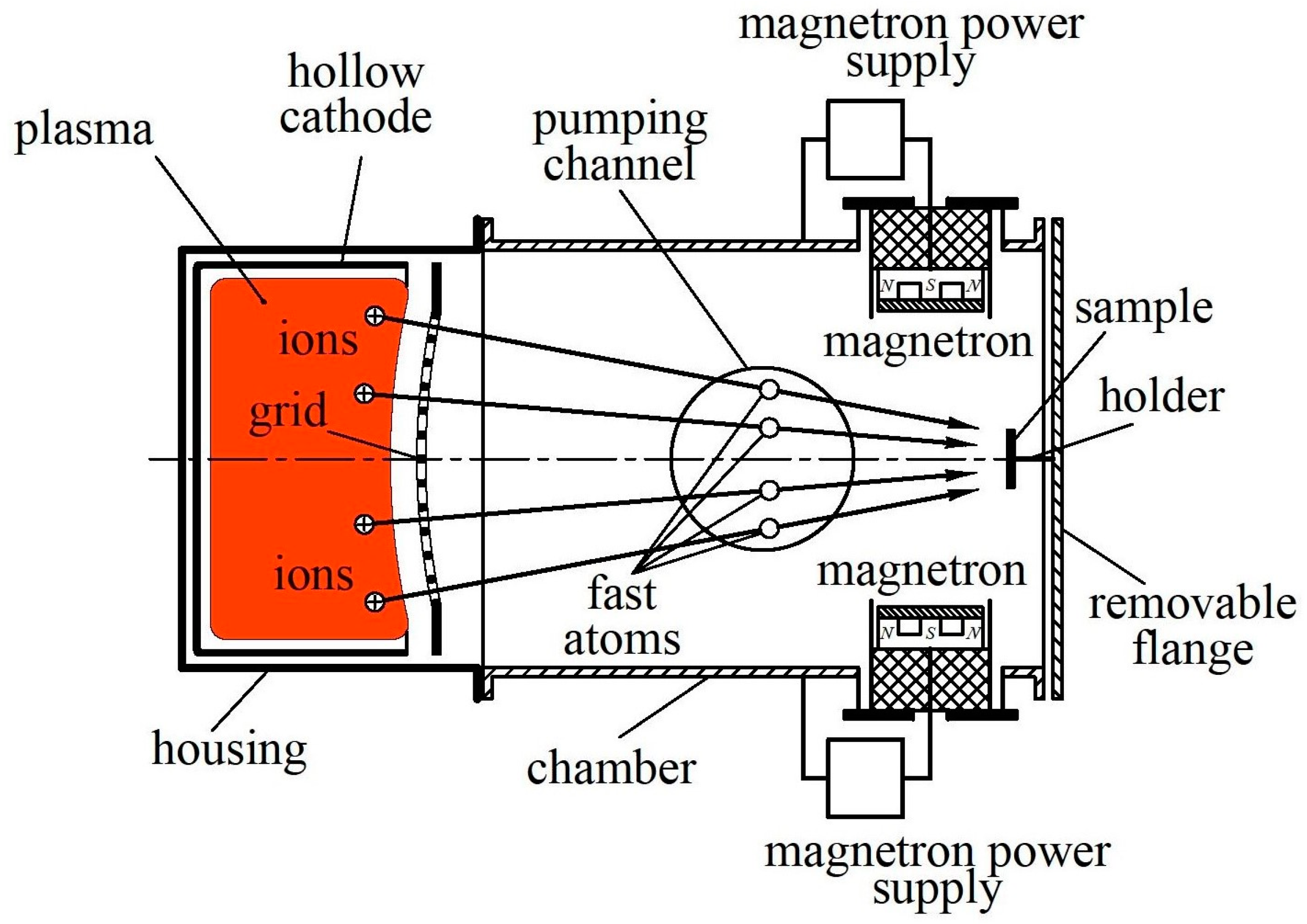
The samples used to carry out the experiments were produced from SiAlON ceramics, were made on a technological unit manufactured by FCT Systeme GmbH (Effelder-Rauenstein, Germany) [10]. Figure 1 presents the experimental system used to process the samples. Its vacuum chamber was 40 cm long and 36 cm in diameter. There was a source of fast atom beams in the chamber. The source comprised a plasma emitter of ions, which filled a cylindrical hollow cathode covered with a concave accelerating grid. The hollow cathode’s diameter was 30 cm and its length amounted to 25 cm. The accelerating grid covered the hollow cathode and the radius of its curvature was 50 cm. There was an anode in the cathode. The positive and negative poles of a discharge power supply were connected, respectively, to the anode and to the hollow cathode. Between the anode and accelerating grid, a high-voltage power supply was connected. Moreover, between the same grid and the chamber, there was a resistor.
A sample holder was fastened to the removable flange of the chamber. The distance between the holder and the grid amounted to 40 cm. To load a sample into the chamber, it was necessary to remove the flange, secure the sample to the holder and then return the flange with the sample to the chamber and pump out the air from it.
The gas was fed into the working vacuum chamber through a hollow cathode and was pumped out through a 20-cm-diameter pumping channel at its bottom. On this chamber wall, a zirconium target was positioned, and, on the opposite wall, there was a pair of titanium magnetron targets (Figure 2). The diameter of both targets was 12 cm. The sample temperature was measured with a pyrometer.
Turning on the power sources caused a glow discharge to occur between the anode and the hollow cathode. Ions from the discharge plasma were accelerated by the grid and, through its holes, entered the chamber. The ion energy was Ei = eU, where U is the accelerating voltage. During collisions with gas molecules, ions receive electrons from them and are transformed into neutrals with the same energy and direction of motion. During charge exchange, slow ions appear. Their charges are neutralized by electrons from the chamber walls. A slow ion current through the resistor generates a negative voltage on the grid, which prevents the penetration into the hollow cathode of electrons from the chamber.
To assess the mean free path of argon ions at an argon pressure of 0.2 Pa, we use the formula λc = 1/noσc, where no = 5 × 10¹⁹ m−3 [11] is the gas density and σc = 2 × 10⁻¹⁹ m2 [12,13] is the charge exchange collision cross-section of argon ions with 5 keV energy. This gives λc = 1/noσc = 0.1 m, which is four times smaller than the gap of 0.4 m between the grid and the sample. For this reason, most of the ions reach the sample surface already converted into neutrals.
The cathode surface area is Sc = 4500 cm2, and, at a current of Ic = 2 A in its circuit, the ion current density is equal to ji = Ic/Sc = 2000/4500 = 0.44 mA/cm2. As the plasma of the discharge has remarkably high homogeneity [14], the current density of the ions accelerated from the plasma toward the grid has the same value. At the grid surface area of Sg = 850 cm2 and transparency of η = 0.75, the current of the accelerated ions from the grid toward the sample is equal to η × ji × Sg = 0.28 A.
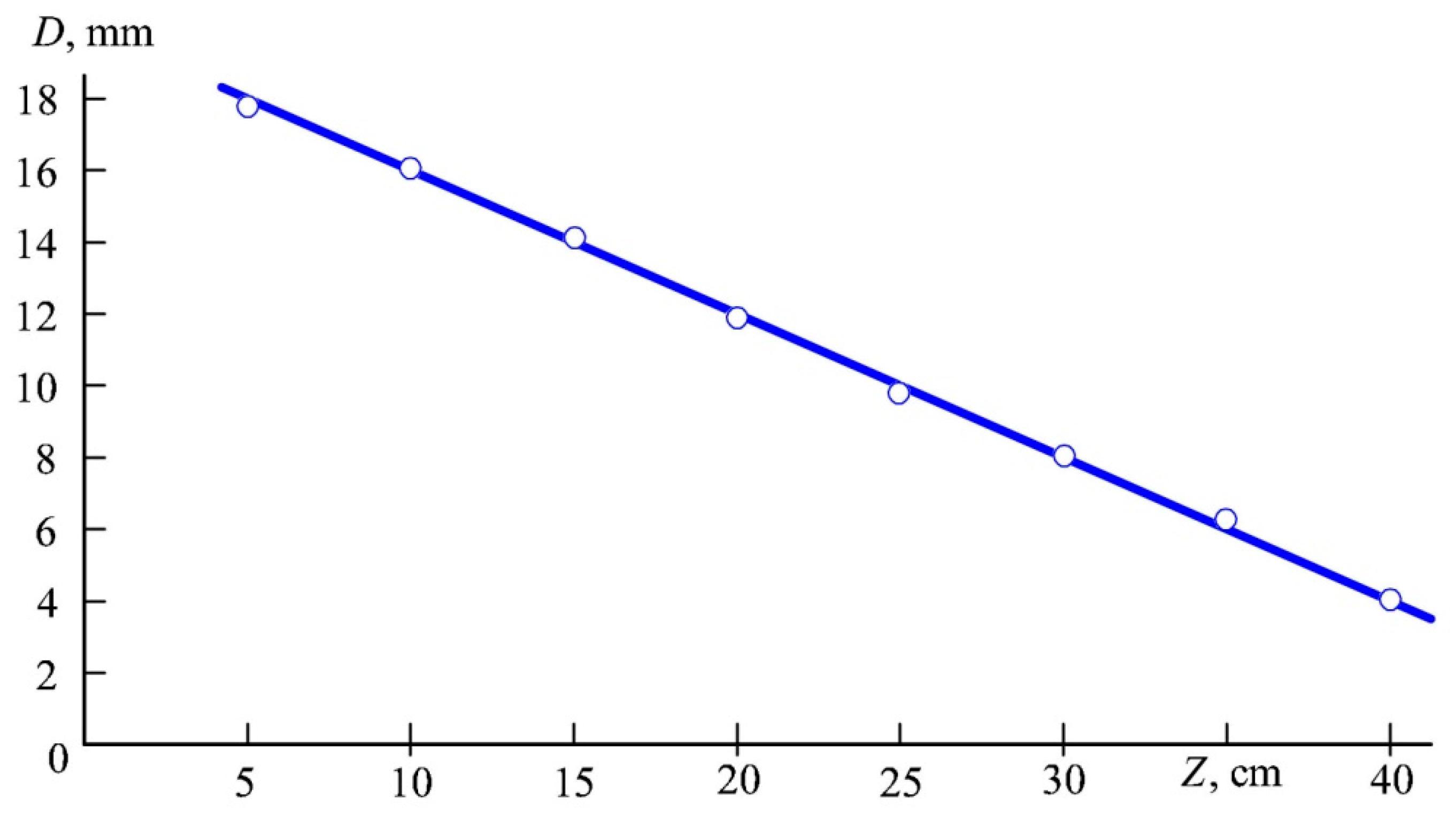
For the assessment of the beam diameter, flat targets were installed on the chamber axis at different distances Z to the grid. The beam imprint diameters D on the targets were measured. Figure 3 shows the dependence of the effective diameter D of a fast atom beam on the distance Z to the grid. With increasing distance Z, diameter D decreases from 18 mm at Z = 5 cm to 4 mm on the holder surface at the distance Z = 40 cm to the grid.
The compression of the beam leads to a decrease in its diameter, from 20 cm near the grid surface to 4.0 cm on the surface of the sample holder, and a decrease in the beam cross-section by 25 times. Consequently, the sputtering rate for the SiAlON samples increases by 25 times, from 0.8 μm/h near the grid surface to 20 μm/h on the surface of the sample holder.
To assess the defectiveness of the surface layer, the “defectiveness index” Id (µm) is used, which is determined by Formula (1). This index is used to compare the levels of defects of the ceramic samples before and after defective layer removal. The scheme and equipment for the measurement of the abrasion resistance are shown in Figure 4.
To assess the abrasion wear resistance of the ceramic samples, we used a Calowear abrasion tester (CSM Instruments SA, Peseux, Switzerland). The wear resistance was higher at a lower rate of formation of spherical cavities (wear spots) on the sample (Figure 4a), which were formed when a rotating ball (counter body) was pressed into the sample. Moreover, an abrasive suspension was constantly supplied to the area between the ball and the sample. The diameter D of the cavity was measured using an optical microscope. When the ball radius R appreciably exceeded D, the volume of worn material was equal to V = π·d4/64R.
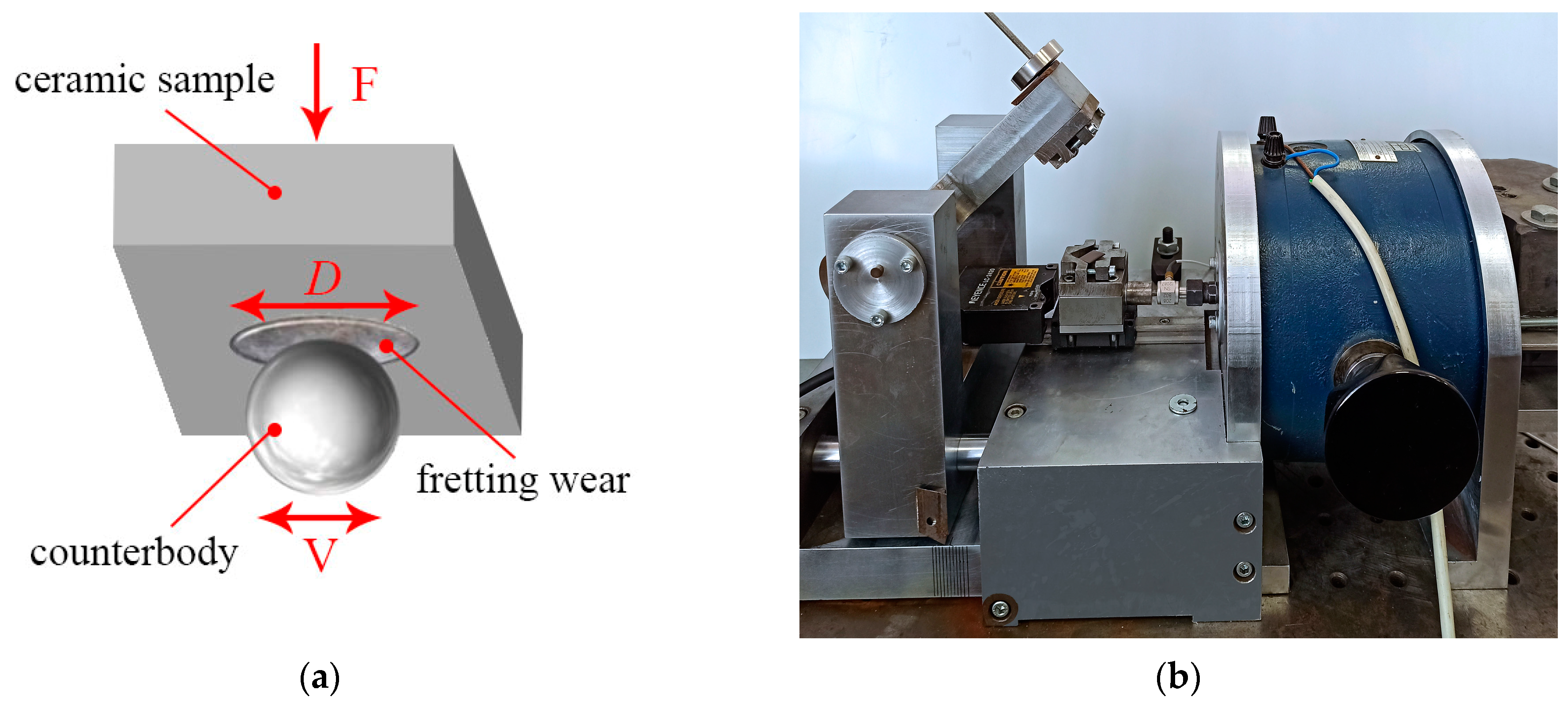
To evaluate the fretting wear resistance, a friction machine model 1401 (Moscow Aviation Institute, Moscow, Russia) was used (Figure 5) [15,16]. Its unique feature is the ability to perform reciprocating movements of the sample in the contact zone using a vibrator.
The ceramic sample remained motionless and the counter body reciprocated. As a result, a wear spot was formed. The investigation of the wear spots and the measurement of their profiles was carried out using a confocal microscope.

3. Results and Discussion

The study of the ceramic samples’ sputtering showed that the thickness of a layer stripped by argon atoms depends on their energy, the flow density and the sample material [17,18,19]. Concerning the sputtering coefficient Y, which is equal to the ratio of the flow of atoms sputtered from the sample to the flow of fast argon atoms striking its surface, it should be noted that Y for single-element substances is always greater than that for chemical compounds of such elements [20,21,22]. As the samples used in the present study were composed of the commercial silicon-nitride-based ceramic SiAlON, the values of the sputtering coefficients obtained using the experimental system presented in Figure 1 and Figure 2 only slightly exceeded Y = 1 (Figure 6). At the same time, the sputtering coefficients of silicon and aluminum with argon ions are several times higher.
To measure the thickness of a layer stripped from the sample surface by fast atoms, half of the sample surface was covered before etching with a flat mask. After etching the sample for 20 min, it was removed from the chamber and, using a Dektak XT stylus profilometer, the step height on the profilogram was measured. It was equal to the thickness Δ of the removed layer.
Figure 6 shows that the sputtering coefficient of SiAlON ceramics rapidly grows when the fast atom energy does not exceed ~3 keV. Further, the increase in the sputtering coefficient slows down. The sputtering coefficient Y increases with the increasing mass of the ions and their energy E. However, at a certain energy E = Emax, it reaches a maximum, and it decreases with the further growth of E [23,24,25]. This is explained by the increase in the depth of the ion penetration into the material of the sample with increasing E. Despite the increase in the number of atoms knocked out by the ions from the crystal lattice, due to the increase in the length of their path to the surface of the sample, the number of atoms capable of reaching it decreases [26,27,28]. Therefore, the optimum energy for the removal of its surface layer should be ~5 keV.
Figure 7 presents the dependence of the removed surface layer thickness Δ on the time t of treatment by fast atoms with 5 keV energy. It shows that the etching depth by argon atoms is proportional to the treatment time. When the current in the anode circuit is reduced from 2 to 1 A, the density of the fast atom flow is decreased by two times and the removed surface layer thickness Δ is also diminished by two times.
The initial roughness of the SiAlON samples measured using the Dektak XT profilometer amounted to Ra = 0.29 µm. During the sample treatment with 5 keV argon atoms, the roughness of its surface slightly decreased and, after treatment for 1 h, it amounted to Ra = 0.14 µm (Figure 8).
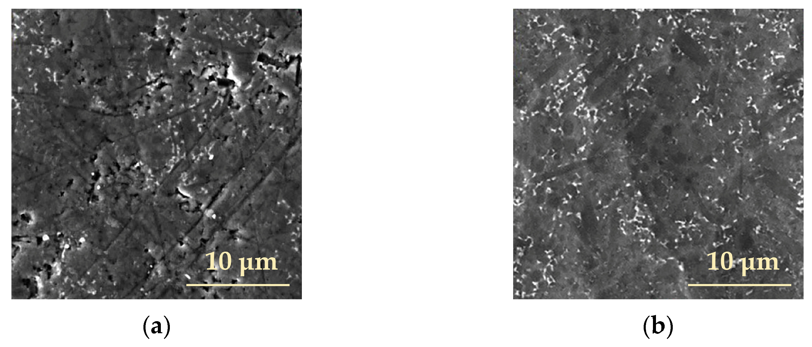
Figure 9 allows the comparison of the sample’s microstructure before the treatment with argon atoms (a) and after a 1-h-long treatment with 5 keV atoms (b). A great number of caverns are seen before the treatment. The size of some caverns reaches 5 µm. There are no caverns seen on the sample surface after the treatment.
In addition to visual differences, various parameters of the surface layer, as shown in Table 1, provide even more convincing evidence of the changes after treatment with fast argon atoms.
The mean values of the defectiveness index for the ceramic samples are obtained on the basis of the measurement results for 10 samples. For comparison, Table 1 also presents the parameters for the samples after diamond grinding (not treated) and polishing.
The experimental results show that etching with argon atoms ensures the near-total stripping of the defective layer and significantly reduces the defectiveness index. These results are extremely significant, because there is no need for expensive equipment [29,30,31]. Argon atom etching provides higher values of surface layer defects than polishing.
The surface layer of the ceramic sample also influences the quality of the subsequently applied coatings. It is seen in Figure 10 that the coating deposited on the ceramic surface without pretreatment with fast argon atoms is replete with numerous defects. This is due to the deterioration of the coating growth conditions [32,33,34,35].
The investigation of the ceramic samples’ abrasive resistance revealed that wear on the samples appeared as a round depression (Figure 11).
The experiments demonstrated a significant reduction in the abrasive wear rate for the SiAlON samples due to the deposition of the coatings. At the same time, the wear resistance of the coatings significantly depends on the state of the sample surface (Table 1). Thus, when testing some coatings applied to defective ceramic samples, their peeling was observed under the influence of an external load [36,37]. Indeed, numerous microstructural defects are clearly visible in the SEM images of their surfaces (Figure 9a). The low adhesion of porous coatings on ceramic surfaces leads to their detachment under mechanical loads.
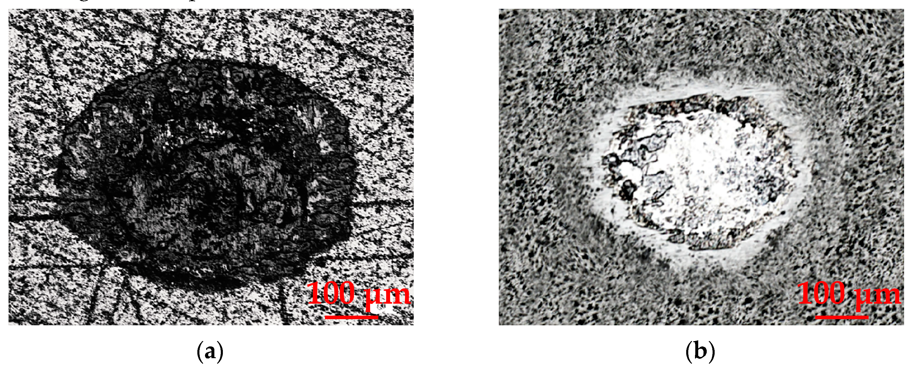
Figure 12 presents photographs of wear spots on the SiAlON samples with TiZrN coatings formed during the fretting tests (Figure 5). It shows that defects on the surface layer significantly increase the fretting wear rate of SiAlON ceramics after 105 friction cycles. It can also be seen that the coating applied before the removal of the defective layer has a larger wear spot size.
The coating applied on the ceramic surface after the removal of the defective layer is remarkable due to its low friction and small amount of wear products. Such coatings, compared to porous coatings, reduce the rate of growth of wear spots. For the original SiAlON ceramic samples, the volumetric wear decreases by 1.4 times when TiZrN coatings are deposited before (a) and by 2.5 times after (b) the removal of the defective layer.

4. Conclusions

1. The removal of defective layers from the surfaces of SiAlON ceramic samples via beams of fast argon atoms ensures etching rates of ~9 µm/h.
2. Etching with 5 keV argon atoms reduces the index of defectiveness of the surface layer by several orders of magnitude and ensures the almost complete removal of the defective layer on SiAlON samples.
3. There are no pores in the TiZrN coatings deposited on the SiAlON ceramic samples after the removal of the defective layers. This significantly increases the wear resistance of the SiAlON ceramic samples.
4. The combined processing of ceramic samples, which comprises the removal of the defective layer and subsequent application of functional coatings, reduces the volumetric wear of SiAlON ceramics with TiZrN coatings by five times.

Author Contributions

Conceptualization, A.S.M., M.A.V. and S.N.G.; methodology, A.S.M. and M.A.V.; software, E.S.M.; validation, A.S.M., M.A.V. and Y.A.M.; formal analysis, Y.A.M.; investigation, E.S.M. and Y.A.M.; resources, E.S.M. and Y.A.M.; data curation, M.A.V. and Y.A.M.; writing—original draft preparation, A.S.M. and M.A.V.; writing—review and editing, A.S.M. and S.N.G.; visualization, E.S.M.; supervision, A.S.M. and S.N.G.; project administration, M.A.V.; funding acquisition, A.S.M. All authors have read and agreed to the published version of the manuscript.

Funding

This research was funded by the Russian Science Foundation, grant no. 23-19-00517.

Institutional Review Board Statement

Not applicable.

Informed Consent Statement

Not applicable.

Data Availability Statement

The data presented in this study are available on request from the corresponding author.

Acknowledgments

The study was carried out with the equipment of the Center of Collective Use of MSUT “STANKIN”.

Conflicts of Interest

The authors declare no conflicts of interest.

References

  1. Zaki, E.G.; Selim, M.S.; Hao, Z.; ElSaeed, S.M.; EL-Saeed, A.M. Special Issue: Recent Trends in Wear and Erosion Resistance of Alloys. Coatings 2023, 13, 64. [Google Scholar] [CrossRef]
  2. Limpichaipanit, A.; Ngamjarurojana, A. Strain Characteristics of PLZT-Based Ceramics for Actuator Applications. Actuators 2023, 12, 74. [Google Scholar] [CrossRef]
  3. Wang, L.; Guo, X.; Zhang, H.; Liu, Y.; Wang, Y.; Liu, K.; Liang, H.; Ming, W. Recent Advances in Superhydrophobic and Antibacterial Coatings for Biomedical Materials. Coatings 2022, 12, 1469. [Google Scholar] [CrossRef]
  4. Xia, T.; Ma, Y.; Zhang, Y.; Li, J.; Xu, H. Effect of Mo and Cr on the Microstructure and Properties of Low-Alloy Wear-Resistant Steels. Materials 2024, 17, 2408. [Google Scholar] [CrossRef]
  5. Dang, M.N.; Singh, S.; Navarro-Devia, J.H.; King, H.J.; Hocking, R.K.; Wade, S.A.; Stephens, G.; Papageorgiou, A.; Wang, J. An Investigation into the Surface Integrity of Micro-Machined High-Speed Steel and Tungsten Carbide Cutting Tools. Micromachines 2023, 14, 1970. [Google Scholar] [CrossRef]
  6. Rizzo, A.; Goel, S.; Luisa Grilli, M.; Iglesias, R.; Jaworska, L.; Lapkovskis, V.; Novak, P.; Postolnyi, B.O.; Valerini, D. The Critical Raw Materials in Cutting Tools for Machining Applications: A Review. Materials 2020, 13, 1377. [Google Scholar] [CrossRef]
  7. Grigoriev, S.N.; Volosova, M.A.; Lyakhovetsky, M.A.; Mitrofanov, A.P.; Kolosova, N.V.; Okunkova, A.A. Technological Principles of Complex Plasma-Beam Surface Treatment of Al2O3/TiC and SiAlON Ceramics. J. Manuf. Mater. Process. 2023, 7, 205. [Google Scholar] [CrossRef]
  8. Li, L. Synergistic Effects of Stress-Rupture and Cyclic Loading on Strain Response of Fiber-Reinforced Ceramic-Matrix Composites at Elevated Temperature in Oxidizing Atmosphere. Materials 2017, 10, 182. [Google Scholar] [CrossRef]
  9. Li, L.; Reynaud, P.; Fantozzi, G. Cyclic-Dependent Damage Evolution in Self-Healing Woven SiC/[Si-B-C] Ceramic-Matrix Composites at Elevated Temperatures. Materials 2020, 13, 1478. [Google Scholar] [CrossRef]
  10. Grigoriev, S.N.; Volosova, M.A.; Fedorov, S.V.; Okunkova, A.A.; Pivkin, P.M.; Peretyagin, P.Y.; Ershov, A. Development of DLC-Coated Solid SiAlON/TiN Ceramic End Mills for Nickel Alloy Machining: Problems and Prospects. Coatings 2021, 11, 532. [Google Scholar] [CrossRef]
  11. McDaniel, E.W. Collision Phenomena in Ionized Gases; John Willey: New York, NY, USA; London, UK, 1964; 775p, Available online: https://scholar.google.com/scholar_lookup?title=Collision+Phenomena+in+Ionized+Gases&author=McDaniel,+E.W.&publication_year=1964 (accessed on 1 September 2024).
  12. Phelps, A.V. Cross sections and swarm coefficients for nitrogen ions and neutrals in N2 and argon ions and neutrals in Ar for energies from 0.1 eV to 10 keV. J. Phys. Chem. Ref. 1991, 20, 557–573. [Google Scholar] [CrossRef]
  13. Phelps, A.V.; Greene, C.H.; Burke, J.P. Collision cross sections for argon atoms with argon atoms for energies from 0.01 eV to 10 keV. J. Phys. B At. Mol. Opt. Phys. 2000, 33, 2965–2981. [Google Scholar] [CrossRef]
  14. Metel, A.S.; Grigoriev, S.N.; Melnik, Y.A.; Prudnikov, V.V. Glow discharge with electrostatic confinement of electrons in a chamber bombarded by fast electrons. Plasma Phys. Rep. 2011, 37, 628–637. [Google Scholar] [CrossRef]
  15. Wood, R.J.K.; Lu, P. Coatings and Surface Modification of Alloys for Tribo-Corrosion Applications. Coatings 2024, 14, 99. [Google Scholar] [CrossRef]
  16. Volosova, M.A.; Lyakhovetsky, M.A.; Mitrofanov, A.P.; Melnik, Y.A.; Okunkova, A.A.; Fedorov, S.V. Influence of Cr-Al-Si-N and DLC-Si Thin Coatings on Wear Resistance of Titanium Alloy Samples with Different Surface Conditions. Coatings 2023, 13, 1581. [Google Scholar] [CrossRef]
  17. Gazia, R.; Chiodoni, A.; Celasco, E.; Bianco, S.; Mandracci, P. X-ray Analysis on Ceramic Materials Deposited by Sputtering and Reactive Sputtering for Sensing Applications. In X-ray Spectroscopy; Sharma, S., Ed.; InTech: London, UK, 2012; pp. 219–241, ISBN 978-953-307-967-7; Available online: https://www.intechopen.com/chapters/27345 (accessed on 1 September 2024).
  18. Seah, M.; Spencer, S.; Shard, A. Depth Resolution, Angle Dependence, and the Sputtering Yield of Irganox 1010 by Coronene Primary Ions. J. Phys. Chem. B 2013, 117, 11885–11892. [Google Scholar] [CrossRef]
  19. Seah, M. Universal Equation for Argon Gas Cluster Sputtering Yields. J. Phys. Chem. C 2013, 117, 12622–12632. [Google Scholar] [CrossRef]
  20. Grigoriev, S.N.; Volosova, M.A.; Okunkova, A.A.; Fedorov, S.V. Influence of Defects in Surface Layer of Al2O3/TiC and SiAlON Ceramics on Physical and Mechanical Characteristics. Ceramics 2023, 6, 818–836. [Google Scholar] [CrossRef]
  21. Seah, M.P.; Spencer, S.J.; Shard, A.G. Angle Dependence of Argon Gas Cluster Sputtering Yields for Organic Materials. J. Phys. Chem. B 2015, 119, 3297–3303. [Google Scholar] [CrossRef]
  22. Korobeishchikov, N.G.; Nikolaev, I.V.; Roenko, M.A.; Atuchin, V.V. Precise sputtering of silicon dioxide by argon cluster ion beams. Appl. Phys. A 2018, 124, 833. [Google Scholar] [CrossRef]
  23. Behrisch, R.; Wittmaack, K.; Hauffe, W.; Hofer, W.O.; Laegreid, N.; McClanahan, E.D.; Sundqvist, B.U.R.; Wittmaack, K.; Yu, M.L. Sputtering by Particle Bombardment III: Characteristics of Sputtered Particles, Technical Applications; Springer: Berlin/Heidelberg, Germany, 1991; Available online: https://scholar.google.com/scholar_lookup?title=Sputtering+by+Particle+Bombardment+III:+Characteristics+of+Sputtered+Particles,+Technical+Applications&author=Behrisch,+R.&author=Behrisch,+R.&author=Wittmaack,+K.&author=Hauffe,+W.&author=Hofer,+W.O.&author=Laegreid,+N.&author=McClanahan,+E.D.&author=Sundqvist,+B.U.R.&author=Wittmaack,+K.&author=Yu,+M.L.&publication_year=1991 (accessed on 1 September 2024).
  24. Grigoriev, S.; Vereschaka, A.; Milovich, F.; Tabakov, V.; Sitnikov, N.; Andreev, N.; Sviridova, T.; Bublikov, J. Investigation of multicomponent nanolayer coatings based on nitrides of Cr, Mo, Zr, Nb, and Al. Surf. Coat. Technol. 2020, 401, 126258. [Google Scholar] [CrossRef]
  25. Mahne, N.; Čekada, M.; Panjan, M. Total and Differential Sputtering Yields Explored by SRIM Simulations. Coatings 2022, 12, 1541. [Google Scholar] [CrossRef]
  26. Cupak, C.; Szabo, P.S.; Biber, H.; Stadlmayr, R.; Grave, C.; Fellinger, M.; Brötzner, J.; Wilhelm, R.A.; Möller, W.; Mutzke, A.; et al. Sputter yields of rough surfaces: Importance of the mean surface inclination angle from nano- to microscopic rough regimes. Appl. Surf. Sci. 2021, 570, 151204. [Google Scholar] [CrossRef]
  27. Lindsey, S.J.; Hobler, G.; Maciążek, D.; Postawa, Z. Simple model of surface roughness for binary collision sputtering simulations. Nucl. Instrum. Methods Phys. Res. Sect. B Beam Interact. Mater. At. 2017, 393, 17–21. [Google Scholar] [CrossRef]
  28. Kelemen, M.; Schwarz-Selinger, T.; Mutzke, A.; Balden, M.; Vassallo, E.; Pedroni, M.; Dellasega, D.; Passoni, M.; Romeo, F.; Hakola, A.; et al. Influence of surface roughness on the sputter yield of Mo under keV D ion irradiation. J. Nucl. Mater. 2021, 555, 153135. [Google Scholar] [CrossRef]
  29. Behrisch, R.; Eckstein, W. Sputtering by Particle Bombardment: Experiments and Computer Calculations from Threshold to MeV Energies; Springer: Berlin/Heidelberg, Germany, 2007; Available online: https://scholar.google.com/scholar_lookup?title=Sputtering+by+Particle+Bombardment:+Experiments+and+Computer+Calculations+from+Threshold+to+MeV+Energies&author=Behrisch,+R.&author=Eckstein,+W.&publication_year=2007 (accessed on 1 September 2024).
  30. Sigmund, P. Six decades of atomic collisions in solids. Nucl. Instrum. Methods Phys. Res. Sect. B Beam Interact. Mater. At. 2017, 406, 391–412. [Google Scholar] [CrossRef]
  31. Wei, Q.; Li, K.-D.; Lian, J.; Wang, L. Angular dependence of sputtering yield of amorphous and polycrystalline materials. J. Phys. D Appl. Phys. 2008, 41, 172002. [Google Scholar] [CrossRef]
  32. Zheng, K.; Li, L.; Dong, Y.; Gao, J.; Hei, H.; Ma, Y.; Zhou, B.; He, Z.; Wang, Y.; Yu, S.; et al. Preparation, Microstructure, Mechanical Properties and Biocompatibility of Ta-Coated 3Y-TZP Ceramic Deposited by a Plasma Surface Alloying Technique. Materials 2020, 13, 1265. [Google Scholar] [CrossRef]
  33. Panjan, P.; Drnovšek, A.; Gselman, P.; Čekada, M.; Panjan, M.; Bončina, T.; Kek Merl, D. Influence of Growth Defects on the Corrosion Resistance of Sputter-Deposited TiAlN Hard Coatings. Coatings 2019, 9, 511. [Google Scholar] [CrossRef]
  34. Lewis, D.B.; Creasey, S.J.; Wüstefeld, C.; Ehiasarian, A.P.; Hovsepian, P.E. The role of the growth defects on the corrosion resistance of CrN/NbN superlattice coatings deposited at low temperatures. Thin Solid Films 2006, 503, 143–148. [Google Scholar] [CrossRef]
  35. Tan, H.; Sun, Q.; Chen, W.; Zhu, S.; Cheng, J.; Yang, J. Tribological performance and wear mechanisms of a high-temperature wear-resistant Al-Si/SiAlON composite. Tribol. Int. 2021, 164, 107227. [Google Scholar] [CrossRef]
  36. Sun, Q.; Yang, J.; Yin, B.; Tan, H.; Liu, Y.; Liu, J.; Cheng, J.; Qiao, Z.; Liu, W. Dry sliding wear behavior of β-Sialon ceramics at wide range temperature from 25 to 800 °C. J. Eur. Ceram. Soc. 2017, 37, 4505–4513. [Google Scholar] [CrossRef]
  37. Acikbas, N.C.; Kara, F. The effect of z value on intergranular phase crystallization of α1/β1-SiAlON-TiN composites. J. Eur. Ceram. Soc. 2017, 37, 923–930. [Google Scholar] [CrossRef]
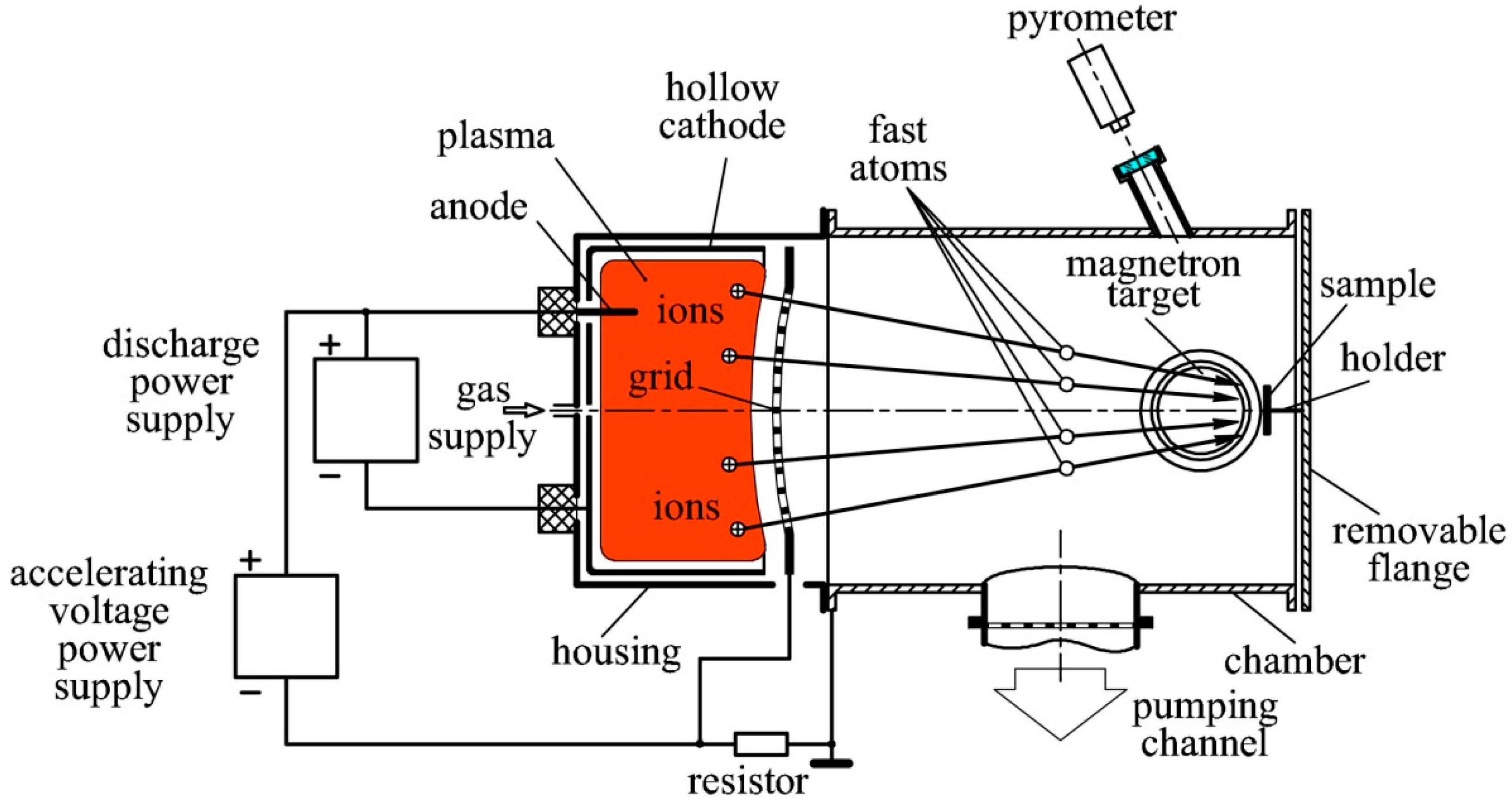
Figure 1. Diagram of the experimental setup.
Surfaces 07 00046 g001
Figure 2. Topside view of the experimental setup.
Surfaces 07 00046 g002
Figure 3. Beam diameter D versus distance to the grid Z.
Surfaces 07 00046 g003
Figure 4. Scheme of the abrasion tests (a) and equipment for the measurement of the abrasion resistance (b).
Surfaces 07 00046 g004
Figure 5. Scheme of the fretting tests (a) and equipment for the measurement of the fretting wear resistance (b).
Surfaces 07 00046 g005
Figure 6. The sputtering coefficient Y versus the energy E of argon atoms.
Surfaces 07 00046 g006
Figure 7. Dependence of the removed layer thickness Δ on the treatment time t at the anode current 2 A (1) and 1 A (2).
Surfaces 07 00046 g007
Figure 8. Profilograms of the SiAlON samples before treatment (a) and after treatment for 1 h with 5 keV argon atoms (b).
Surfaces 07 00046 g008
Figure 9. SEM images of the SiAlON samples before treatment (a) and after treatment with fast argon atoms (b).
Surfaces 07 00046 g009
Figure 10. SEM images of TiZrN coatings deposited on the samples before (a) and after (b) treatment with fast argon atoms.
Surfaces 07 00046 g010
Figure 11. Profilograms of wear spots after 20 min of abrasive exposure on samples composed of SiAlON ceramics with TiZrN coatings deposited before (a) and after (b) treatment with fast argon atoms.
Surfaces 07 00046 g011
Figure 12. Wear spots after 105 cycles of friction of counter body with SiAlON samples coated with TiZrN before (a) and after (b) treatment with fast argon atoms.
Surfaces 07 00046 g012
Table 1. Parameters of the surface layer conditions of SiAlON samples after various types of processing.
Type of ProcessingParameter of the Surface
Density of Defects ρMaximum Depth of Defective Layer Rt, µmIndex of Defectiveness
ρ∙Rt, µm
Roughness Parameter Ra, µm
Diamond grinding0.333.271.080.29
Treatment with 5 keV argon atoms for 1 h0.010.460.00460.14
Diamond grinding, finishing and polishing0.0040.380.00150.014
Disclaimer/Publisher’s Note: The statements, opinions and data contained in all publications are solely those of the individual author(s) and contributor(s) and not of MDPI and/or the editor(s). MDPI and/or the editor(s) disclaim responsibility for any injury to people or property resulting from any ideas, methods, instructions or products referred to in the content.