Proceeding Paper

On-Chip Thermal Insulation Using Porous GaN †

1
Engineering Department, University of Cambridge, Cambridge CB3 0FA, UK
2
Department of Materials Science and Metallurgy, University of Cambridge, Cambridge CB3 0FS, UK
*
Author to whom correspondence should be addressed.
Presented at the Eurosensors 2018 Conference, Graz, Austria, 9–12 September 2018.
Proceedings 2018, 2(13), 776; https://doi.org/10.3390/proceedings2130776
Published: 10 December 2018
(This article belongs to the Proceedings of EUROSENSORS 2018)

Abstract

:
This study focuses on the thermal characterization of porous gallium nitride (GaN) using an extended 3ω method. Porous semiconductor materials provide a solution to the need for on-chip thermal insulation, a fundamental requirement for low-power, high-speed and high-accuracy thermal sensors. Thermal insulation is especially important in GaN devices, due to the intrinsically high thermal conductivity of the material. The results show one order of magnitude reduction in thermal conductivity, from 130 W/mK to 10 W/mK, in line with theoretical predictions for porous materials. This achievement is encouraging in the quest for integrating sensors with opto-, power- and RF-electronics on a single GaN chip.

1. Introduction

GaN is an increasingly popular material for semiconductor devices, building on its success in optoelectronics and high electron mobility transistors (HEMT) for RF and power applications. More recently, GaN has also been investigated as technology platform for sensing applications [1], due to its enhanced robustness against thermal, mechanical, chemical and radiation damage. For example, many of these efforts are supported by demand for solid-state sensors able to monitor chemical processes, mechanical processing, and outer space exploration. Creating novel materials and understanding their thermal characteristics are important steps in the development of thermal sensors based on GaN technology.
Thermal sensors are a broad class of sensing devices, including temperature sensors, thermal flow sensors, infra-red emitters and detectors, micro-hotplate based chemo-resistive and catalytic gas sensors, and thermal inertial sensors. Such devices usually include a small active region delimited from the rest of the substrate material by thermal insulation. The performance of thermal sensors is correlated with the ability to minimise the thermal mass of—and the heat conduction from the active region, these parameters impacting directly the sensor accuracy, thermal transient times and power consumption. The employment of porous materials is a viable route to achieve such objectives as well as concurrently facilitate monolithic integration of thermal sensors with additional electronic components such as HEMTs or optoelectronics.
Heat conduction through semiconductor materials impacts the operation of electronic devices beyond thermal sensors. Consequently, thermal tests are required for both the development and the quality-assurance of electronic devices. Electrical-only techniques for measuring thermal characteristics are advantageous from a practical perspective, implying lower equipment requirements and allowing the integration of thermal tests with other electrical tests. Such a technique, the 3ω method [2,3], was exploited in this work for measuring the thermal conductivity of porous GaN.

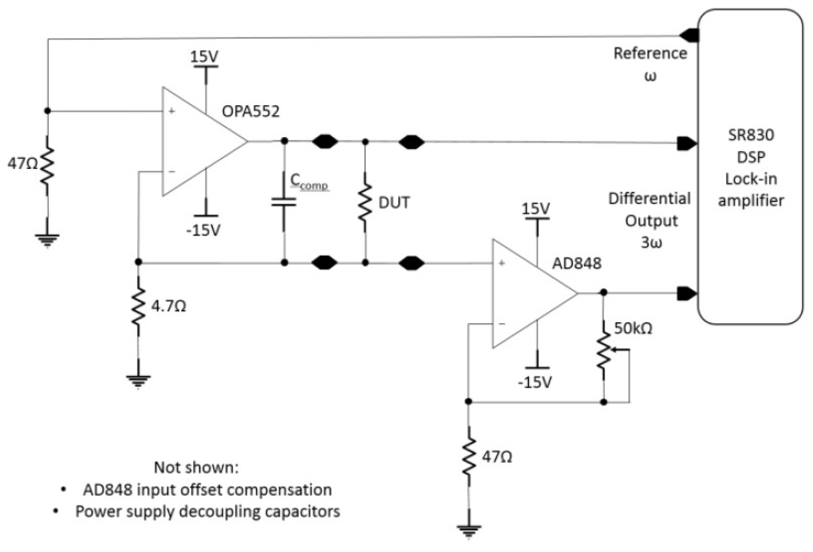
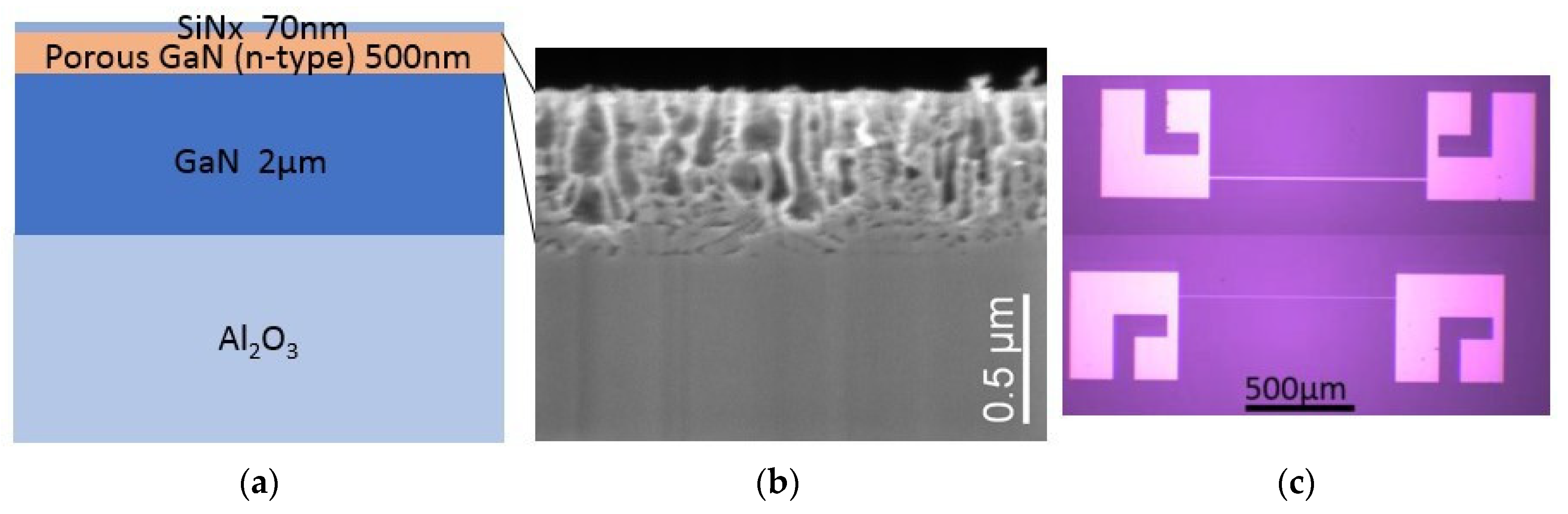
2. Materials and Methods

The sample used in this study was produced by metalorganic chemical vapour deposition (MOCVD) of GaN on a 2-inch sapphire substrate. A 2 μm-thick unintentionally doped layer of (0001) GaN was deposited first, followed by 500 nm of n-type doped GaN. The full sample structure is shown in Figure 1a, where the top SiNx layer was deposited at a later fabrication stage. A wafer- scale electrochemical process [4] was used to porosify selectively the n-type doped GaN layer without changing the crystal structure of the semiconductor material, hence minimizing the impact on its structural integrity. Figure 1b shows the result of the porosification, with the majority of the pores forming branching vertical channels, which are roughly aligned with the c-axis of the GaN crystal. Other pore sizes and densities can be obtained by varying the n-type doping level and the electrochemical process parameters.
A 70 nm-thick layer of SiNx was deposited onto the samples by PE-CVD for electrical insulation, followed by single-step lithography to create a template for the test structures. Thin lines of metal were deposited on the SiNx layer, as shown in Figure 1c, for performing the 3ω thermal characterization. Two types of test lines were used, with 5 μm and 10 μm widths respectively, both types being 1 mm in length. These metal lines acted as both localized heaters and RTD-type temperature sensors [2], while the dual-line setup was required for differentiating the thermal characteristics of the thin porous layer from those of its solid substrate [3]. Finally, a thin Ti adhesion layer and a 150 nm-thick layer of Ni were deposited on the patterned substrates by electron-beam PVD, followed by the removal of excess metal. The electrical and thermal effects of the Ti adhesion layer and the SiNx electrical insulation can be neglected due to their reduced thickness compared with the Ni and substrate layers, respectively.
The electrical measurements were performed at 20 °C under high vacuum at pressure levels below 10−4 Torr to minimize the heat conduction through air. The measurement setup included a Stanford Research 830 (SR830) lock-in amplifier, custom interface electronics specific to the 3ω method, and shielded connections to reduce external noise injection and internal cross-talk. The custom electronics, shown in Figure 2, include a low-noise high-power voltage-controlled current source (VCCS) for creating a clean sinusoidal excitation current, and a low-noise Vω compensation amplifier. The latter circuit is required for compliance with the differential input voltage range of the lock-in amplifier. Frequency sweeps between 4 Hz and 4096 Hz were performed with sinusoidal signals of 3 Vrms for both, the 5 μm- and 10 μm-wide test structures.

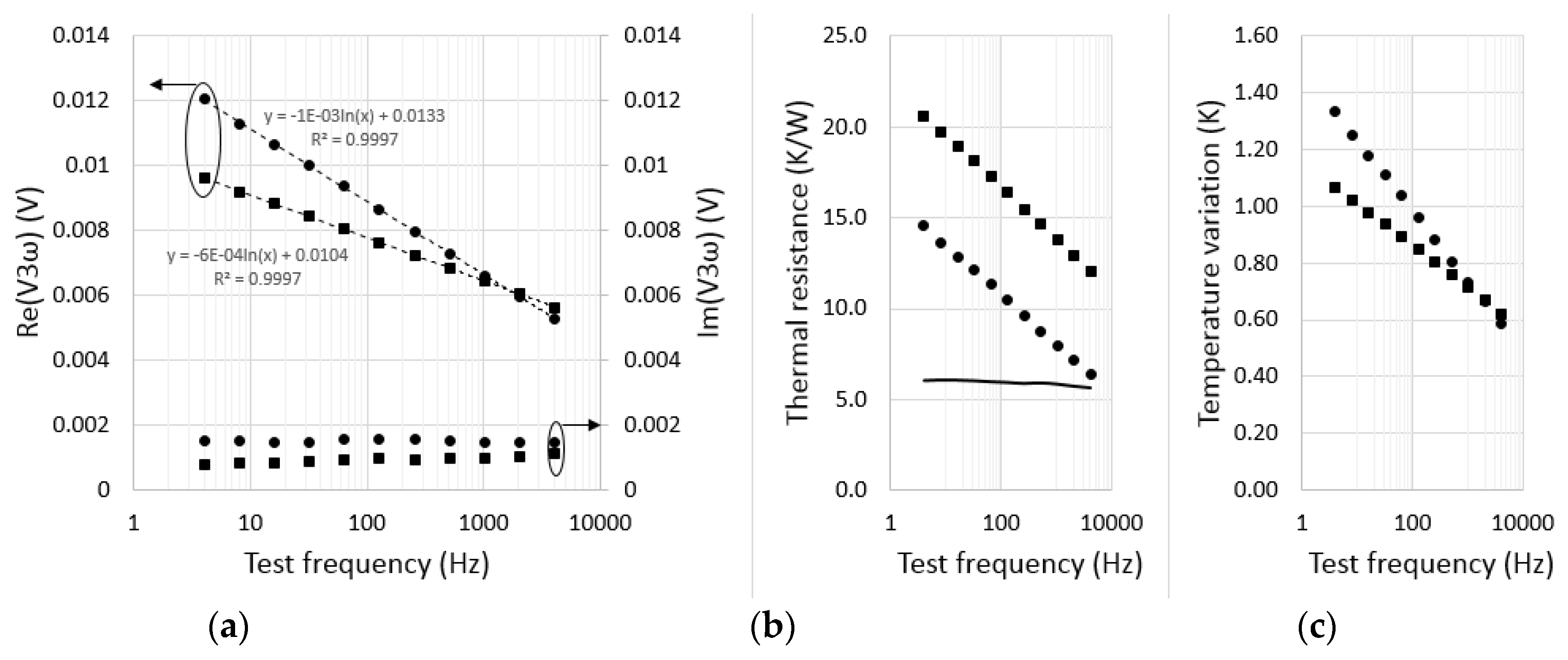
3. Results and Discussion

The primary results are the real and imaginary magnitudes of the third-harmonic signal (V3ω), shown in Figure 3a. The linear reduction of Re(V3ω) with the logarithm of test frequency and the stationary behavior of Im(V3ω) are hallmarks of this characterization method. By extracting the semi- log gradient of Re(V3ω), the thermal conductivity observed in each of the two structures were calculated as 123 W/mK and 131 W/mK for the 5 μm and 10 μm structures respectively, indicating that both test structures interrogate primarily the non-porous GaN substrate and measure its high thermal conductivity. However, the extended 3ω method [3] allows the determination of the thermal conductivity of the superficial porous layer based on the difference between thermal resistances and the geometry of the test structures:
λ porous = t 21 × ( 1 / b 1 ) - ( 1 / b 2 ) ( R sensor 1 th - R sensor 2 th ) - ( ln ( b 2 / b 1 ) / 2 π l λ substrate )
where t is the thickness of the layer of interest, l is the length of the test structures, b1 and b2 are their respective half-widths, and Rth is the thermal resistance measured by each of the test lines. This approach is validated by the constant difference in thermal resistance across the frequency test range, shown in Figure 3b. By measuring this difference as 5.6–6.1 K/W, and using 130 W/mK as λsubstrate, the thermal conductivity of the porous GaN layer was calculated as 10.0 ± 0.5 W/mK. The data were processed assuming that the TCR of Ni is constant and equal to 0.006 K−1, as the temperature fluctuations were less than 2 K throughout the experiment, as shown by Figure 3c.
This result agrees with the theories summarized by Smith et al. [5] for porous materials. For instance, using Landauer’s relation [6], shown in Equation (2), and considering an average volumetric porosity of 0.6, the expected thermal conductivity is approximately 13 W/mK. Landauer’s relation is preferred since it includes the effect of random distribution of pore geometry, predicting more accurate values than a simpler parallel-paths thermal analysis, which returns thermal conductivity estimates decreasing linearly with volumetric porosity. However, precise quantitative determination of thermal conductivity by theoretical means is not possible for samples with great variation in pore size and distribution.
λ = 1 4 [ λ p ( 3 v p 1 ) + λ s ( 2 3 v p ) + ( λ p ( 3 v p 1 ) + λ s ( 2 3 v p ) ) 2 + 8 λ s λ p ]
where λp and λs are the thermal conductivity values for the porous and solid material, respectively, and vp is the volumetric pore fraction.

4. Conclusions

The thermal conductivity of a thin porous GaN layer was analyzed in an electrical-only custom test setup using an extended 3ω method for isolating the analysis to the top 500 nm of the sample. The results, showing more than one order of magnitude reduction in thermal conductivity, from 130 W/mK to 10 W/mK, confirm the theoretical expectations of significant conductivity reduction with porosity, supporting the use of porous GaN in high-performance thermal sensing and in integrated circuits where thermal insulation is required. Future work includes the study of samples with different pore characteristics and crystal orientations, and the optimization of porous GaN properties for thermal sensors.

Funding

This work was supported by the Engineering and Physical Sciences Research Council [EP/L015889/1], the EPSRC Impact Acceleration Account Follow on Fund of the University of Cambridge, and the Innovate UK [103446] GaNSense project.

Acknowledgments

The authors gratefully acknowledge the assistance of N. C. A. van-Fraassen and P.W. Oluwasanya with sample processing and the help of D. Purdie and Y. Li in operating the probing station.

Conflicts of Interest

The authors declare no conflict of interest. The founding sponsors had no role in the design of the study; in the collection, analyses, or interpretation of data; in the writing of the manuscript, and in the decision to publish the results.

References

  1. Udrea, F.; De Luca, A. CMOS technology platform for ubiquitous microsensors. In Proceedings of the 2017 International Semiconductor Conference (CAS), Sinaia, Romania, 11–14 October 2017; pp. 43–52. [Google Scholar] [CrossRef]
  2. Cahill, D.G. Thermal conductivity measurement from 30 to 750 K: The 3ω method. Rev. Sci. Instrum. 1990, 61, 802–808. [Google Scholar] [CrossRef]
  3. Alvarez-Quintana, J.; Rodriguez-Viejo, J. Extension of the 3ω method to measure the thermal conductivity of thin films without a reference sample. Sens. Actuators A Phys. 2008, 142, 232–236. [Google Scholar] [CrossRef]
  4. Zhu, T.; Liu, Y.; Ding, T.; Fu, W.Y.; Jarman, J.; Ren, C.X.; Oliver, R.A. Wafer-scale Fabrication of Non-Polar Mesoporous GaN Distributed Bragg Reflectors via Electrochemical Porosification. Sci. Rep. 2017, 7, 45344. [Google Scholar] [CrossRef] [PubMed]
  5. Smith, D.S.; Alzina, A.; Bourret, J.; Nait-Ali, B.; Pennec, F.; Tessier-Doyen, N.; Gonzenbach, U.T. Thermal conductivity of porous materials. J. Mater. Res. 2013, 28, 2260–2272. [Google Scholar] [CrossRef]
  6. Landauer, L. The electrical resistance of binary metallic mixtures. J. Appl. Phys. 1952, 23, 779–784. [Google Scholar] [CrossRef]
Figure 1. Experimental sample: (a) sample structure; (b) SEM image of the porous GaN layer; (c) optical photograph of the 3ω test structures and their Kelvin-connection pads.
Proceedings 02 00776 g001
Figure 2. Custom electronics for 3ω thermal characterization, including a high-power amplifier (OPA552) configured as a VCCS and a low-noise compensation amplifier (AD848).
Proceedings 02 00776 g002
Figure 3. Experimental data vs. frequency for the 5 μm (squares) and 10 μm (circles) test line: (a) complex 3ω signal; (b) thermal resistance (line indicates the difference between the two sets of data); (c) amplitude of temperature variation.
Proceedings 02 00776 g003
Publisher’s Note: MDPI stays neutral with regard to jurisdictional claims in published maps and institutional affiliations.

