Proceeding Paper

Universal Integrated Photodetector Platform †

Department of Micro- & Nanosystems, University of Applied Sciences Wr. Neustadt, A-2700 Wr. Neustadt, Austria
*
Author to whom correspondence should be addressed.
Presented at the Eurosensors 2018 Conference, Graz, Austria, 9–12 September 2018.
Proceedings 2018, 2(13), 756; https://doi.org/10.3390/proceedings2130756
Published: 10 December 2018
(This article belongs to the Proceedings of EUROSENSORS 2018)

Abstract

:
Within this work we developed a universal integrated photodetector platform for the detection, amplification and digitalization of various optical data signals. The concept features two internal plus two external photodiodes, signal amplification and output stages each. For each application a combination of the optimal input detector, the suitable amplifier plus gain setting and the appropriate output stage can be combined individually.

1. Chip Concept

Depending on the application, specific optical sensors are available for well-defined optical conditions like fast datacom receivers or very sensitive detectors. However, the requirements concerning receiving wavelength, bandwidth or sensitivity might change during use, [1]. Hence settings often have to be changed. The aim of the proposed detector platform is to enable easy changes in the setup as required by the application. This includes the use of different photodetectors or signal processing methods, e.g., integration instead of amplification. The concept features four optical inputs, four signal amplification options and four output stages to be connected individually. For the optical inputs two internal photodiodes plus two external photodetector inputs are implemented. The amplification block contains two transimpedance amplifiers in addition to an active and a passive integrator stage with switchable gain in each of the four amplifiers.
The output stage consists of four selectable drivers: two analog drivers for different loads, an analog feed through and a 10 bit dual-slope analog-to-digital converter (ADC). These main blocks are connected via two switchable analog 4:4 multiplexers. For each application a combination of the optimal input detector, the suitable amplifier including a selectable gain setting and the appropriate output stage can be combined individually. The complete chip concept is shown in Figure 1.

2. Optical Sensor Design

2.1. Photodetection

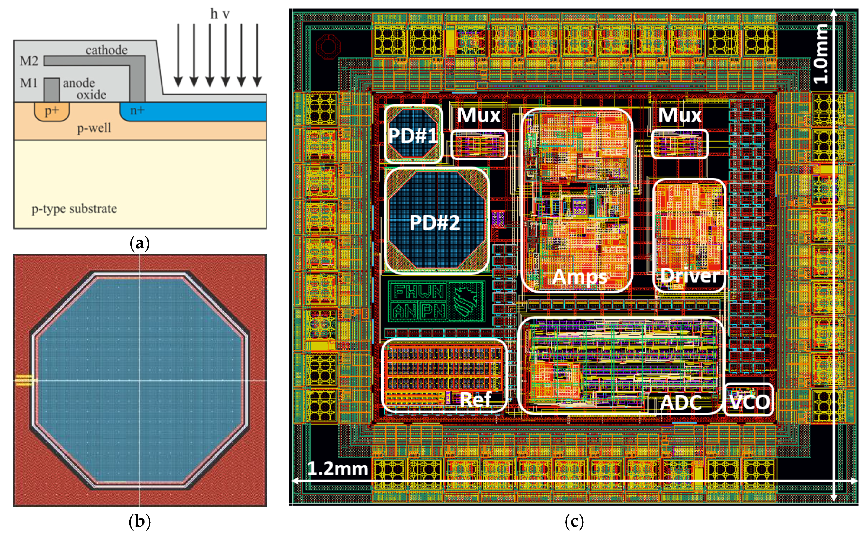
Opto-Electronic Integrated Circuits (OEIC) with on-chip photodiodes are superior to multi-chip solutions because of better signal quality due to low parasitic components from missing chip interconnects as well as simplified packaging efforts. Common standard CMOS technology features PN-junctions for the integration of PN-photodiodes applicable as optical detectors. Based on the setup of n-channel field effect transistors (N-FET), lateral PN-photodiodes can be realized using the highly N+ doped source region forming the cathode and the P doped well of the bulk region with highly P+ doped substrate contacts forming the anode, see Figure 2. Considering these available doping concentrations, a relatively thin Space-Charge Region (SCR) with thickness of dSCR ~ 1 µm is formed at the maximum possible bias voltage Vdd = 5 V of the process. According to LAMBERT-BEER’s law P(y) = P0 exp(–αy) with the absorption coefficient for visible light in silicon of α ~ 1 µm−1, the relevant absorption depth is in the range of up to y = 10 µm. Thus only a certain part of the photogenerated charge carriers is generated in the fast, drift dominated SCR, while the other electron-hole pairs slowly diffuse to the electrode. This diffusion contribution limits the bandwidth of PN-photodiodes to fPN ~ 20–50 MHz as well as the quantum efficiency. Advanced photodetectors like PIN-diodes require special BiCMOS-processes, but feature high bandwidth fPIN > 1 GHz together with high responsivity. Photodiodes in III/V-semiconductor technology like GaAs, InP, InSb, GaN with smaller bandgap energy on the other hand ensure near infrared detection. Therefore, the two realized internal PN-photodiodes with a diameter of Ø = 100 µm/200 µm can be completed by appropriate external PIN- or III/IV-diodes depending on the application. The equivalent circuit diagram of the photodiodes in Figure 3 contains an optically controlled current source representing the photogeneration term and the junction capacitance.

2.2. Amplification

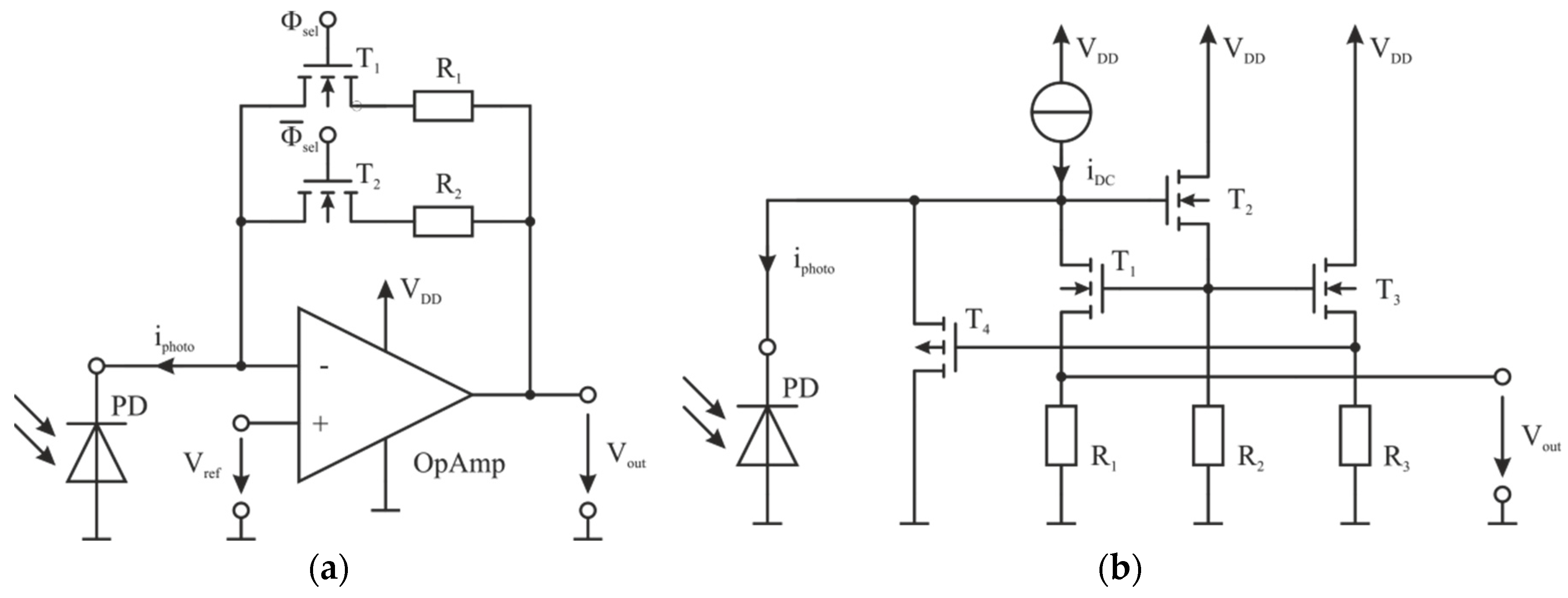
The signal amplification stage can be chosen by switching to either a TransImpedance Amplifier (TIA), a ReGulated Cascode (RGC) amplifier, an active or a passive integration stage. The TIA converts the current of the photodiode iphoto into an output voltage vout. The circuit uses a reference voltage Vref to bias the photodiode and is connected in inverting configuration of the two stage MILLER compensated Operational Amplifier (OpAmp) with selectable gain using feedback resistors R = 1 kΩ/10 kΩ, see Figure 4a. Thus a bandwidth of f = 280 MHz/28 MHz is achieved.
The amplifier with the RGC circuit is shown in Figure 4b. The two inner transistors T1,2 form together with the transistor pair T13,4 and the current source the regulated cascoded amplifier according to the proposed concept in [2]. This simple circuit has a fixed gain of R = 5 kΩ and achieves a bandwidth of f = 33 MHz. Due to the simple circuit concept, the RGC features a reduced power consumption compared to the TIA.
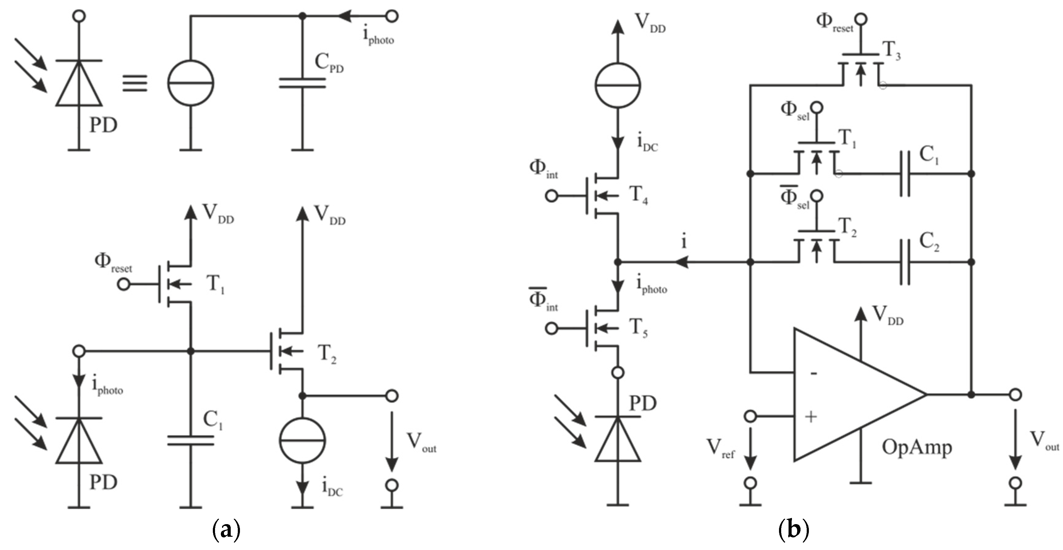
Both integration stages are realized with a selectable integration capacitor C = 1 pF/10 pF each, see Figure 3: The passive integrator is based on the active pixel circuit containing the photodiode, the capacitor C, a reset transistor T1 and the amplifier T2 in common source configuration. The active integrator not only contains the OpAmp in inverting configuration with reset T3 and selectable integration capacitor, but also features an optional dual slope mode. Due to the implemented DC current source with selectable fixed current, both up and down-integration over the full voltage range is possible.

2.3. Functional Blocks

The signal routing is done with two integrated 4:4 analog multiplexers. The selected signal path can be controlled by a 4 bit logic, two for input and two for output selection. The bilateral switching elements have to feature a relative low on-impedance over the whole voltage range. This is realized using transmission gates with complementary switching transistors. Furthermore, different single ended analog drivers in source follower configuration with output impedance of R = 1 kΩ/1 MΩ plus feedthrough are realized. A 50 Ω-impedance driver has not been implemented due to power consumption reasons. Together with the active integration stage an integrated dual-slope analog-to-digital converter (ADC) [3] with 10 bit and 250 kSps is realized. Therefore, an integrated comparator triggers a dedicated digital counter if the integration limits are reached. This counter reading directly corresponds to the detected signal value which has now been converted into the time domain. Therefore, it provides the options of either an internal tunable clock generator based on a Voltage Controlled Oscillator (VCO) or and an external clock input. The ADC serially shifts out the converted sampled digital values.

3. Summary

We presented the concept of a universal integrated photodetector platform with focus on high flexibility towards diverse applications. Therefore, the concept combines several options for photodetection, amplification, gain setting and signal output as an Opto-Electronic Integrated Circuit (OEIC) realized as a System-On Chip (SOC). This chip is fabricated in 0.18 mm CMOS technology. Figure 2 shows the setup and the layout of the integrated photodiode plus the complete chip layout with 40 pads and a chip area of A = 1.2 mm2. Table 1 shows the simulated key data of the chip.

Acknowledgments

The chip-fabrication is supported by the Europractice Chip Design Competition.

References

  1. Neumann, P. Design eines multifunktionalen integrierten optischen Sensorchips für universelle Anwendungen in 0.18 µm CMOS-Technologie. Bachelor’s Thesis, Univ. Applied Sciences Wr. Neustadt, Wiener Neustadt, Austria, 2017. [Google Scholar]
  2. Kim, Y.; Lee, S. A 72 dBO 11.43 mA novel CMOS regulated cascode TIA for 3.125 Gb/s optical communications. In Proceedings of the IEEE 26th International SOC Conference, Erlangen, Germany, 4–6 September 2013. [Google Scholar]
  3. Gamauf, C.; Nemecek, A.; Leisenberger, F. Design and Characterization of an integrated 10 bit Analog to Digital Converter for 100 MSps in 0.18 µm CMOS. In Proceedings of the Austrochip Conference 2014, Graz, Austria, 9 October 2014. [Google Scholar]
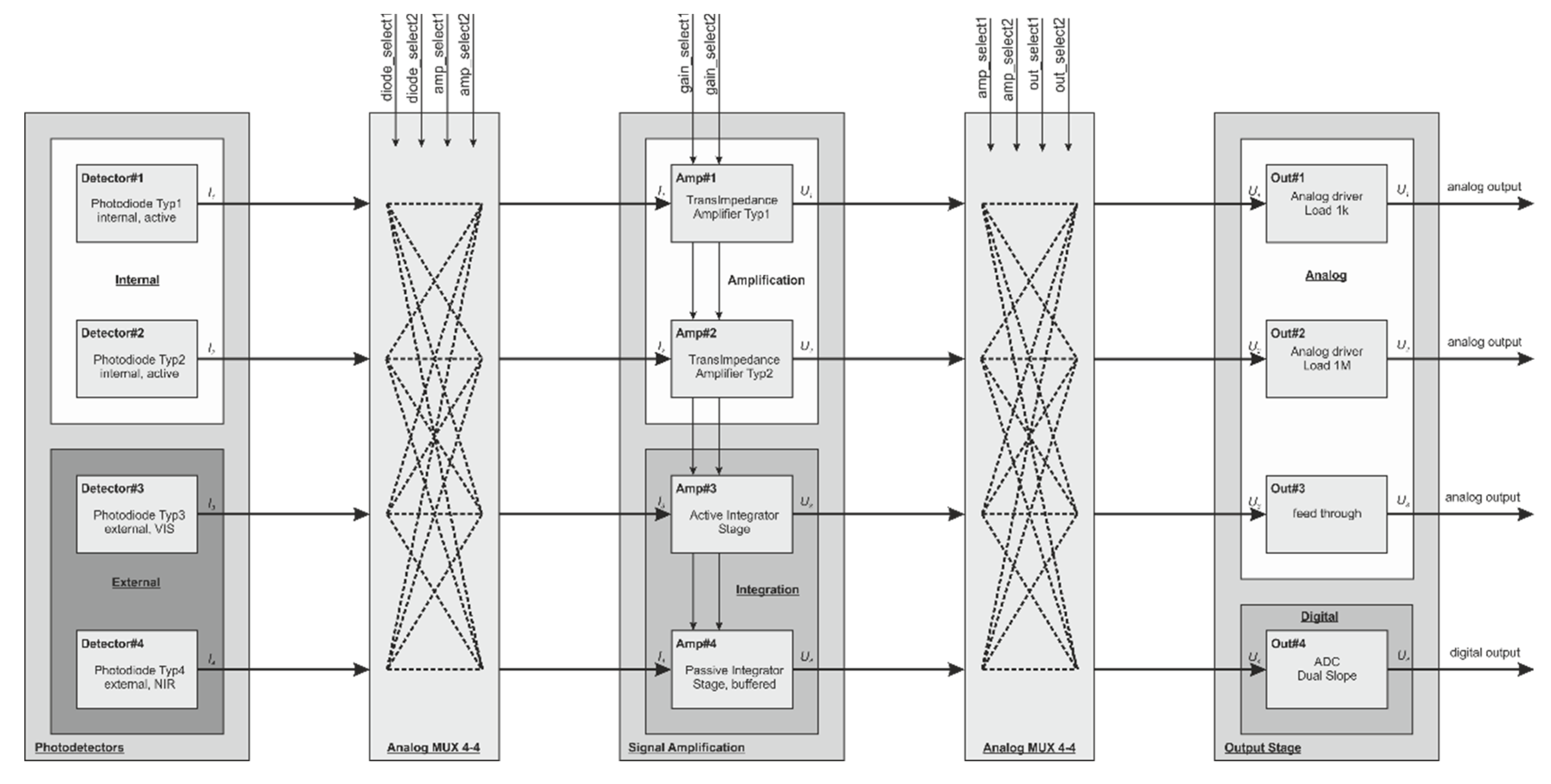
Figure 1. Universal Integrated Photodetector Platform—Functional block diagram.
Proceedings 02 00756 g001
Figure 2. Universal Integrated Photodetector Platform: (a) photodiode cross section, (b) photodiode layout and (c) complete chip layout with highlighted functional blocks.
Proceedings 02 00756 g002
Figure 3. Integration stages: (a) passive and (b) active dual slope integration.
Proceedings 02 00756 g003
Figure 4. Amplification stage: (a) Transimpedance and (b) Regulated Cascode amplifier.
Proceedings 02 00756 g004
Table 1. Key data of the sensor—simulation values.
Key Data
Photodiodeinternal & external
 internal PN-diodesØ = 100 µm/200 µm
AmplificationIntegrator & TIA
 Integrator active/passiveC = 1 pF/10 pF
 GainR = 1 kΩ/5 kΩ/10 kΩ
 TIA & RGCf = 280 MHz/28 MHz
Outputanalog & digital
 Output driverR = 1 kΩ/1 MΩ
Dual-slope ADC10 bit @ 250 kSps
Signal routing2 x 4:4 MUX
Supply5 V/<20 mA
Technology0.18 mm CMOS
 # Pads40
 Chip areaA = 1.2 mm2
Publisher’s Note: MDPI stays neutral with regard to jurisdictional claims in published maps and institutional affiliations.