

Article

Electro-Thermal Coupled Modeling of SPADs Considering Avalanche Self-Heating Effects

1
Jiangsu Provincial Key Laboratory of MEMS Sensors and ASIC Manufacturing Technology, School of Integrated Circuits, Jiangnan University, Wuxi 214401, China
2
Department of Electrical, Electronic and Computer Engineering, The University of Western Australia, Crawley 6009, Australia
*
Author to whom correspondence should be addressed.
Inventions 2026, 11(3), 45; https://doi.org/10.3390/inventions11030045
Submission received: 13 March 2026 / Revised: 30 April 2026 / Accepted: 1 May 2026 / Published: 4 May 2026

Abstract

The performance of single-photon avalanche diodes (SPADs) is highly dependent on the operating temperature, while traditional SPAD models neglect the self-heating effect induced by avalanche current during long-term device operation, leading to insufficient prediction accuracy. This paper proposes an electro-thermal coupled SPAD simulation model that self-consistently integrates the transient thermal effects of the avalanche process with temperature-dependent electrical parameters, including junction capacitance, breakdown voltage, impact ionization coefficients, and Shockley–Read–Hall (SRH) recombination rates. The complete electro-thermal coupled model is constructed based on Sentaurus-TCAD thermal simulation and Virtuoso circuit simulation and implemented via the Verilog-A language. Simulation results demonstrate that after the device operates for 100 μs under repeated avalanche-quenching processes, the self-heating effect causes a 0.34 V shift in breakdown voltage, increases the device dead time by 3.34 ps, and simultaneously reduces the photon detection probability and elevates the dark count rate. This study conducts a systematic investigation into the performance degradation mechanism of SPAD devices induced by the self-heating effect, laying a theoretical foundation at the device self-heating level for subsequent research on the electrothermal interaction between quenching circuits and device bodies.

1. Introduction

Solid-state LiDAR has become a core component of autonomous driving perception systems, and SPADs have become the mainstream optical receivers owing to their high sensitivity, fast response and low power consumption [1,2,3,4]. However, there is currently a lack of accurate SPICE-compatible models for SPAD devices, forcing circuit designers to carry out optimization through costly trial and error; in addition, the self-heating effect produced during long-term avalanche operation degrades device performance and may even cause device failure. Therefore, establishing an electro-thermally coupled SPAD model is crucial for realizing thermal effect prediction, supporting simulation-based design, and further promoting the industrial development of solid-state LiDAR.
Early SPAD models developed by researchers such as Dalla Mora [5] and Zappa [6] employed analog circuits using basic components to simulate photon detection behavior but suffered from limited accuracy. Subsequent works by Mita [7] and He [8] adopted Verilog-A hardware description language to construct SPAD circuit models, significantly improving modeling efficiency. However, these circuit-based approaches failed to effectively simulate critical parameters such as photon detection probability (PDP) and dark count rate (DCR). To address these limitations, Giustolisi [9] proposed behavioral models for predicting SPAD noise characteristics. Yet, behavioral models lack a close physical correlation with internal device physics, limiting simulation accuracy. Maciazek [10] and Klauner [11] subsequently introduced TCAD simulation tools to strengthen the physics-based foundation, effectively enhancing model fidelity. Despite these advances, existing SPAD modeling research has predominantly focused on electrical performance while overlooking self-heating effects. Current self-heating studies concentrate primarily on MOSFET and electrostatic discharge (ESD) devices. For instance, El-Dakroury et al. [12] developed a double-gate LDMOS compact model incorporating two-dimensional surface potential and self-heating effects. Pan et al. [13] analyzed hot spot distributions across different ESD layout configurations, while Wang et al. [14] constructed an ESD self-heating model to systematically investigate performance degradation mechanisms. Notably, the self-heating in SPADs originates from the temperature accumulation in the junction region during long-term avalanche-quenching cycles and is therefore different from the device self-heating caused by ESD stress.
This paper proposes an electro-thermal coupling modeling method for SPADs that self-consistently integrates the transient thermal effects of the avalanche process with temperature-dependent electrical parameters, including junction capacitance, breakdown voltage, impact ionization coefficients and SRH recombination rates. The impact ionization coefficients characterize the photon avalanche probability of the device, and the SRH recombination rates describe the variation in thermal carriers in the device, from which the evolution of the dark count rate can be derived. The established model accurately predicts the influence of self-heating effects on the core performance indicators of SPADs. Simulation verification based on practical device layouts shows that lattice temperature variations caused by long-term avalanche-quenching cycles significantly change the junction capacitance, breakdown voltage, photon detection probability and dark count rate of the device. Compared with traditional SPICE models, the electro-thermal coupling model can predict the actual operating characteristics of the device and satisfy the requirements of large-scale system-level simulations.

2. Materials and Methods

2.1. SPAD Electrical Model

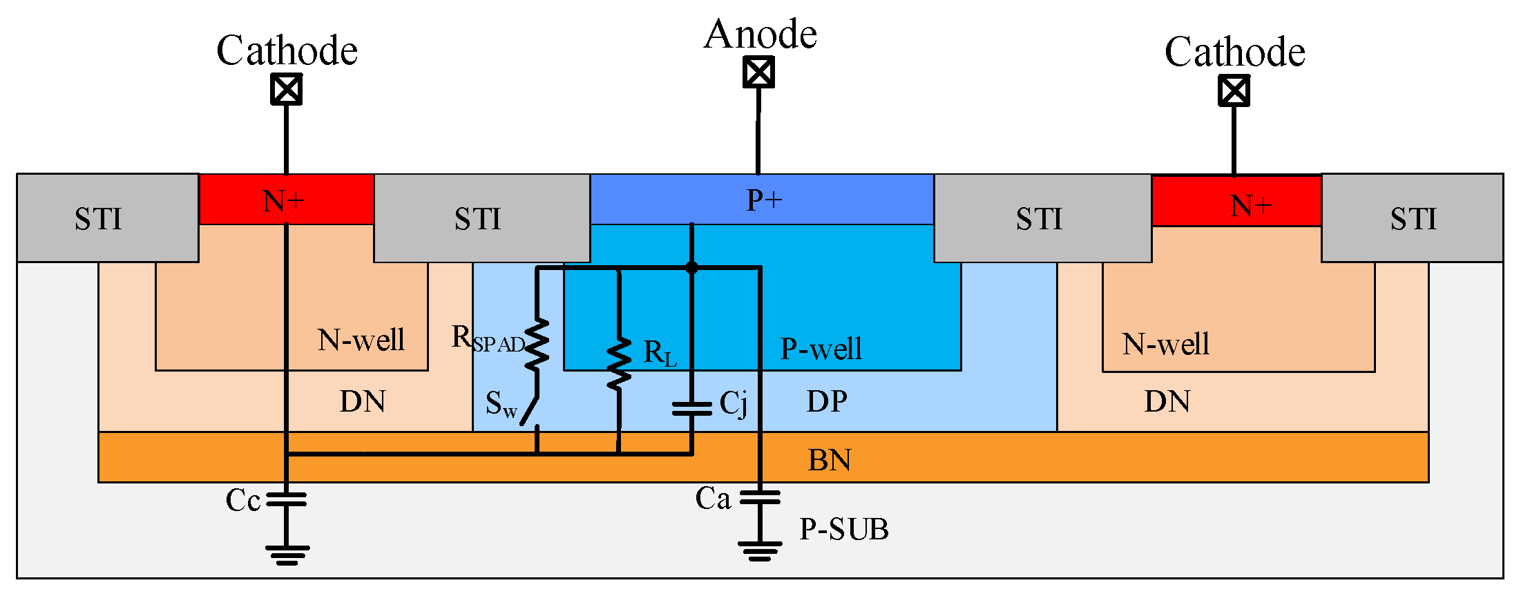
A SPAD device was fabricated based on a 0.18 μm BCD process in this study, and its structure is illustrated in Figure 1, where BN denotes the Buried N-well, DN denotes the Deep N-well, DP denotes the Deep P-well, and STI denotes Shallow Trench Isolation. Based on this structure, a precise SPAD device simulation model was proposed. When the device operates in the non-conducting state, switch S w remains open, and only resistor R L provides a leakage current path. When the device operates in Geiger mode and absorbs photons to trigger an avalanche, S w closes, forming a parallel breakdown resistor, R b r e a k , with R S P A D and R L to generate avalanche current. Junction capacitance C j and stray capacitances C a / C c characterize the AC dynamic characteristics of the device, governing the high-frequency response and transient behavior under varying voltage conditions.

2.1.1. Temperature-Dependent Junction Capacitance

Temperature fluctuations induced by the self-heating effect significantly affect the junction capacitance, C j , of SPAD devices. The temperature dependence of this capacitance involves complex physical mechanisms arising primarily from depletion layer width variations. Its temperature characteristics can be described by Equation (1) [15].
C j = C j 0 · [ 1 + m · ( A c · ( T T 0 ) V j V j 0 V j 0 ) ]
where C j 0 represents the junction capacitance value at room temperature, m is the temperature coefficient, A c is a specific fitting coefficient, V j is the instantaneous junction potential, and V j 0 is the initial junction potential. For SPAD devices, the increased junction capacitance extends the quenching and recovery cycle of the avalanche process, leading to increased dead time, which reduces detection efficiency and timing accuracy.

2.1.2. Temperature-Dependent Breakdown Voltage

The breakdown voltage of SPAD devices can be expressed by Equation (2). According to the physical relationships shown in Equations (2) and (3), the temperature dependence of the breakdown voltage of SPAD devices mainly comes from the variations in built-in potential V b i .
V B D = ε 0 ε r E c r i t 2 2 q N D · ( N A + N D N A ) V b i
In Equation (2), ε 0 is the vacuum dielectric constant, ε r is the relative dielectric constant of silicon, and E c r i t is the critical electric field strength. N A is the acceptor doping concentration, N D is the donor doping concentration, and V b i is the built-in potential. The temperature dependence of the V b i can be described by the following relationship:
V b i = k B T q · l n ( N A N D n i 2 )
In Equation (3), k B represents the Boltzmann constant, where T is the temperature, q is the elementary charge, and n i is the intrinsic carrier concentration. It can be concluded that V b i is mainly influenced by N A , N D , and n i . Among these, n i exhibits strong temperature sensitivity, and its temperature variation characteristic is described in Equation (4).
n i ( T ) = A · T 3 2 · exp ( E g ( T ) 2 k B T q )
where A is a temperature-dependent empirical coefficient. From Equation (4), the intrinsic carrier concentration presents a strong exponential dependence on temperature and is closely correlated with the bandgap width. As the temperature increases, the bandgap-narrowing effect occurs in silicon materials, which directly changes E g ( T ) . Meanwhile, the Fermi level shifts toward the midgap position and reshapes the carrier distribution in the conduction and valence bands, further affecting the generation of intrinsic carriers. The variation in E g with temperature can be quantitatively calculated by Equation (5):
E g ( T ) = E g ( 0 ) α S i · T 2 T + β S i
This bandgap formula is an empirical formula that describes the variation in the bandgap width of semiconductor materials with temperature. In the formula, E g ( T ) denotes the bandgap width at temperature T , with the unit eV; E g ( 0 ) represents the bandgap width at absolute zero. α S i and β S i are characteristic constants related to the silicon material. It is indicated that as the temperature increases, the term α S i · T 2 T + β S i rises accordingly, and the bandgap width E g ( T ) of the semiconductor decreases gradually, which reflects the nonlinear relationship between bandgap width and temperature.

2.1.3. SPAD Current Model

To accurately describe the current characteristics of SPAD devices, Equation (6) is introduced to solve the convergence problem in the current calculation near the breakdown voltage region [8].
I S P A D = I s + V n R b r e a k · ln ( 1 + e V e x V n )
The SPAD current, I S P A D , mainly includes the pre-avalanche reverse saturation current, I s , and the avalanche-generated current component, with the latter related to overbias voltage, V e x , and the device empirical coefficient, V n . Traditional models use fixed on-resistance, causing abrupt current changes near breakdown voltage and hindering transient simulation convergence; thus, this model introduces a nonlinear resistance mechanism, greatly improving the device’s transient convergence in this key region. In short, SPAD’s self-heating alters its junction capacitance and breakdown voltage. These changes bring dynamic junction capacitance and overbias voltage to the SPAD, which sharply reduces LiDAR reliability. Therefore, research on the electro-thermal coupled model is urgently needed.
Temperature variations induced by self-heating affect not only junction capacitance and breakdown voltage but also significantly impact two core performance parameters of SPAD devices: PDP and DCR.

2.1.4. Temperature-Dependent Physical Quantities in PDP

The avalanche probability of SPAD is jointly determined by the electron avalanche probability, P e , triggered in the P neutral region and the hole avalanche probability, P h , triggered in the N neutral region. According to the McIntyre model, the combined avalanche probability, P j , can be characterized by the following equation.
P j = P e + P h P e P h
The overall avalanche probability of the device can be obtained by calculating and adding up the avalanche probabilities along different electric field distribution paths. It is specifically expressed by the following Equation (8).
P j ( s ) = P h ( 0 ) · f ( s ) P h ( 0 ) · f ( s ) + 1 P h ( 0 )
Here, s represents the trajectory length of the electric field line. P h ( 0 ) is the hole avalanche probability at s = 0 . f ( s ) is a function used to quantify the impact of the electric field and carrier transport processes on avalanche gain. It is shown in Equation (9).
f ( s ) = exp [ 0 s ( α e α h ) d s ]
The electron and hole ionization coefficients, α e and α h , use the Bologna University impact ionization model. This model is based on impact ionization data generated by the Boltzmann solver HARM. It is suitable for a wider range of electric field intensity and temperature. Its model expression is given by the following equation [16]:
α ( E , T ) = E a ( T ) + b ( T ) exp [ d ( T ) E + c ( T ) ]
where E denotes the local electric field strength in the avalanche multiplication region, and a ( T ) , b ( T ) , c ( T ) , and d ( T ) are the temperature-dependent empirical parameters calibrated for silicon. The ionization coefficients of this model are mainly affected by the temperature-dependent parameters a ( T ) , b ( T ) , c ( T ) and d ( T ) . These parameters are all polynomial functions of temperature T . Their values increase with the rise in temperature. This makes the ionization coefficients show a trend of decreasing as temperature increases.
Photon detection in a SPAD begins with photon-absorption-generating photocarriers, which then drift to the high-electric-field depletion region to accumulate energy. Subsequently, successive impact ionization is induced within the depletion region, ultimately triggering avalanche breakdown. The key performance metric, photon detection probability, is defined as the probability that a single photon absorbed in the depletion region initiates a detectable avalanche signal. Essentially, this parameter is jointly determined by the SPAD’s quantum efficiency ( Q E ) and the joint avalanche probability ( P j ), as expressed in Equation (11) [17].
P D P = Q E ( λ ) · P j
For quantum efficiency, assuming that a single absorbed photon generates one electron–hole pair, the quantum efficiency is equal to the ratio of the number of photons absorbed in the collection region to the number of incident photons. Its mathematical expression is given by Equation (12) [18].
Q E ( λ ) = N t o p ( λ ) N b o t ( λ ) N i n ( λ )
In the equation above, N i n ( λ ) denotes the incident photon flux, N t o p ( λ ) represents the photon flux at the silicon surface, and N b o t ( λ ) stands for the photon flux at the interface between the junction region and the substrate, respectively.

2.1.5. Temperature-Dependent Physical Quantities in DCR

For the research on DCR, since the main reason why DCR is affected by temperature is thermally generated electron–hole pairs, namely, thermal carriers [19], this study will ignore the contributions of dark counts caused by the band-to-band tunneling mechanism and trap-assisted tunneling mechanism when analyzing the temperature dependence of DCR. The generation mechanism of thermal carriers is mainly described by the SRH recombination theory, and its equation is as follows [20]:
R S R H = n p n i 2 τ p ( n + n 1 ) + τ n ( p + p 1 )
Here, R S R H denotes the SRH net recombination rate, n and p are electron concentration and hole concentration respectively, τ n is electron minority carrier lifetime, and τ p is hole minority carrier lifetime, while n 1 and p 1 are the trap-induced equivalent carrier concentrations. n 1 = N c e x p ( E t E c k B T ) and p 1 = N v exp ( E v E t k B T ) , where N c is the effective density of states in the conduction band, N v is the effective density of states in the valence band, E c is the conduction band edge energy, E v is the valence band edge energy, and E t is the trap energy level. The DCR of SPAD devices can be calculated by Equation (14). First, this equation calculates the total number of thermal carriers by integrating the SRH recombination rate over the entire device volume. Then, it multiplies the total amount by the avalanche probability. In this way, it can characterize the total occurrence rate of avalanche events triggered by thermal carriers.
D C R = V d e v R S R H · P j d V d e v
In Equation (14), V d e v is the volume of the SPAD device. Based on the above analysis of temperature-dependent ionization coefficients and SRH recombination rates, it is known that the change in PDP primarily results from the influence of dynamic ionization coefficients, while the change in DCR primarily results from the influence of dynamic SRH recombination rates. These changes lead to a sharp drop in the signal-to-noise ratio (SNR) of LiDAR, making it unable to meet the core requirements of high sensitivity and high accuracy for LiDAR in scenarios such as autonomous driving and environmental monitoring. Therefore, research on the SPAD electro-thermal coupling model is crucial. Table 1 lists the parameters used in the model for reference. All parameter values are obtained from relevant manuals or through tests.

2.2. SPAD Self-Heating Model

2.2.1. Thermodynamic Model

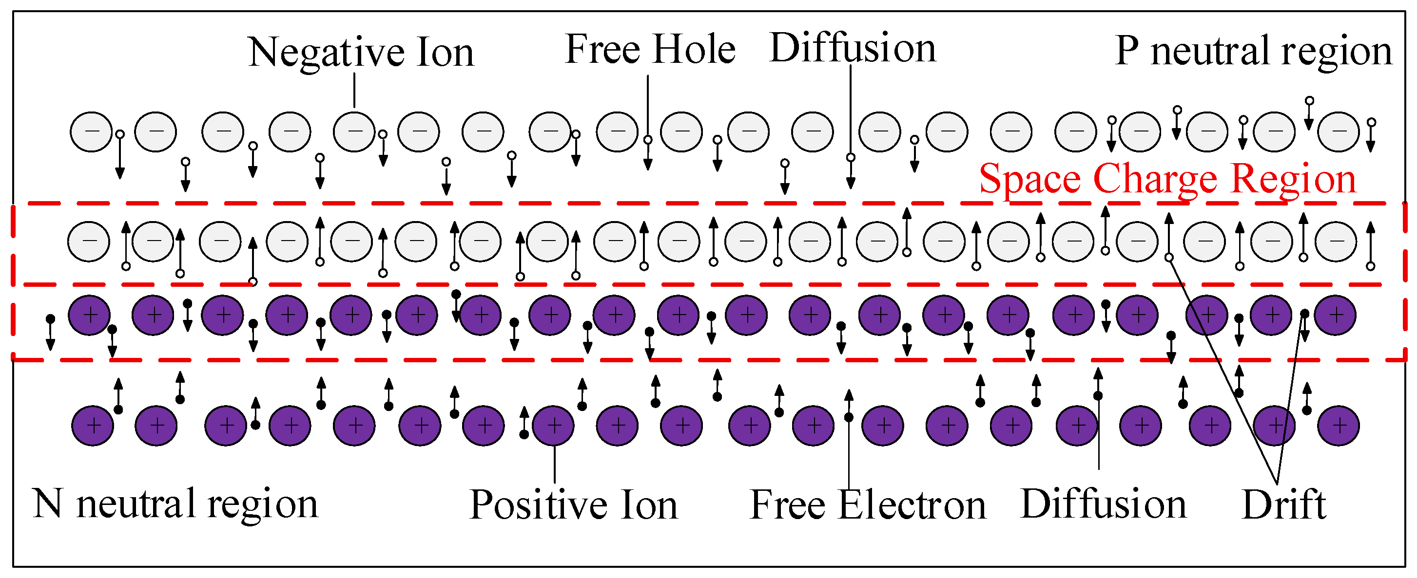
As shown in Figure 2, the purple circles represent positive donor ions distributed in the N-type neutral region and on the N-side of the space charge region. The gray circles denote negative acceptor ions, which are immobile negative charges located in the P-type neutral region and on the P-side of the depletion region. In addition, the small black and white dots with arrows stand for mobile charge carriers that undertake electrical conduction and participate in the avalanche multiplication process. Under reverse bias conditions, electron and hole drift motion occurs in the depletion region of the PN junction due to the built-in electric field. In the P neutral region and the N neutral region, carrier diffusion motion occurs. At this time, the diffusion motion and drift motion exist in a state of dynamic equilibrium. When a single photon is incident on the depletion region and excites carriers, these carriers continue to accelerate in the strong electric field. The acquired kinetic energy generates additional electron–hole pairs through impact ionization.
When describing the charge transport relationship inside the SPAD devices under isothermal conditions, the drift-diffusion physical model is generally used to represent the electron and hole current densities. They are shown in Equations (15) and (16).
J n = n q μ n V F n
J p = p q μ p V F p
Here, V F n and V F p represent the gradients of electron and hole quasi-Fermi potentials, respectively. Considering that the SPAD avalanche self-sustaining phenomenon will cause a rapid local temperature rise of the device, the carrier transport processes inside the SPAD cannot be simply regarded as an isothermal condition. Therefore, the following thermodynamic model equations, Equations (17) and (18), are used to represent the electron and hole current densities [21].
J n = n q μ n ( V F n + P n T )
J p = p q μ p ( V F p + P p T )
Here, T represents the temperature variation gradient, and P n and P p are the absolute thermopower [22]. At this time, in addition to solving the Poisson equation and the current continuity equation under the thermodynamic model, it is also necessary to solve the heat flow equation of the internal lattice of the device, as shown in the following equation:
c T t · κ T = · [ ( P n T + V F n ) J n + ( P p T + V F p ) J p ] ( E c + 3 2 k B T ) · J n             ( E v 3 2 k B T ) · J p + q R ( E c E v + 3 k B T )
In Equation (19), c is the volumetric heat capacity. κ denotes the lattice thermal conductivity, which has a value of 1.422 W · c m 1 · K 1 at 300 K [23]. The term c T t describes the variation in lattice temperature, while · κ T corresponds to the lattice heat conduction term. The expression · [ ( P n T + V F n ) J n + ( P p T + V F p ) J p ] refers to the carrier heat flux, which reflects the heat transfer accompanying carrier transport. In addition, q R ( E c E v + 3 k B T ) represents the heat generation density induced by carrier recombination, which quantifies the thermal energy released during electron–hole pair recombination in SPAD.
The above equations can simultaneously calculate the mechanisms of lattice self-thermal conduction, carrier transport and the effect of carrier recombination on lattice energy. They effectively make up for the limitations of traditional models, allowing the thermodynamic model to more accurately describe the temperature variation law of SPAD devices caused by avalanche current. On this basis, subsequent simulations use the Sentaurus-TCAD software (Y-2026.03) as the platform and rely on the above-optimized thermal model to carry out systematic research and quantitative analysis on the self-heating effect of SPAD devices, providing more reliable theoretical support for device performance optimization.

2.2.2. Sentaurus-TCAD Thermal Simulation

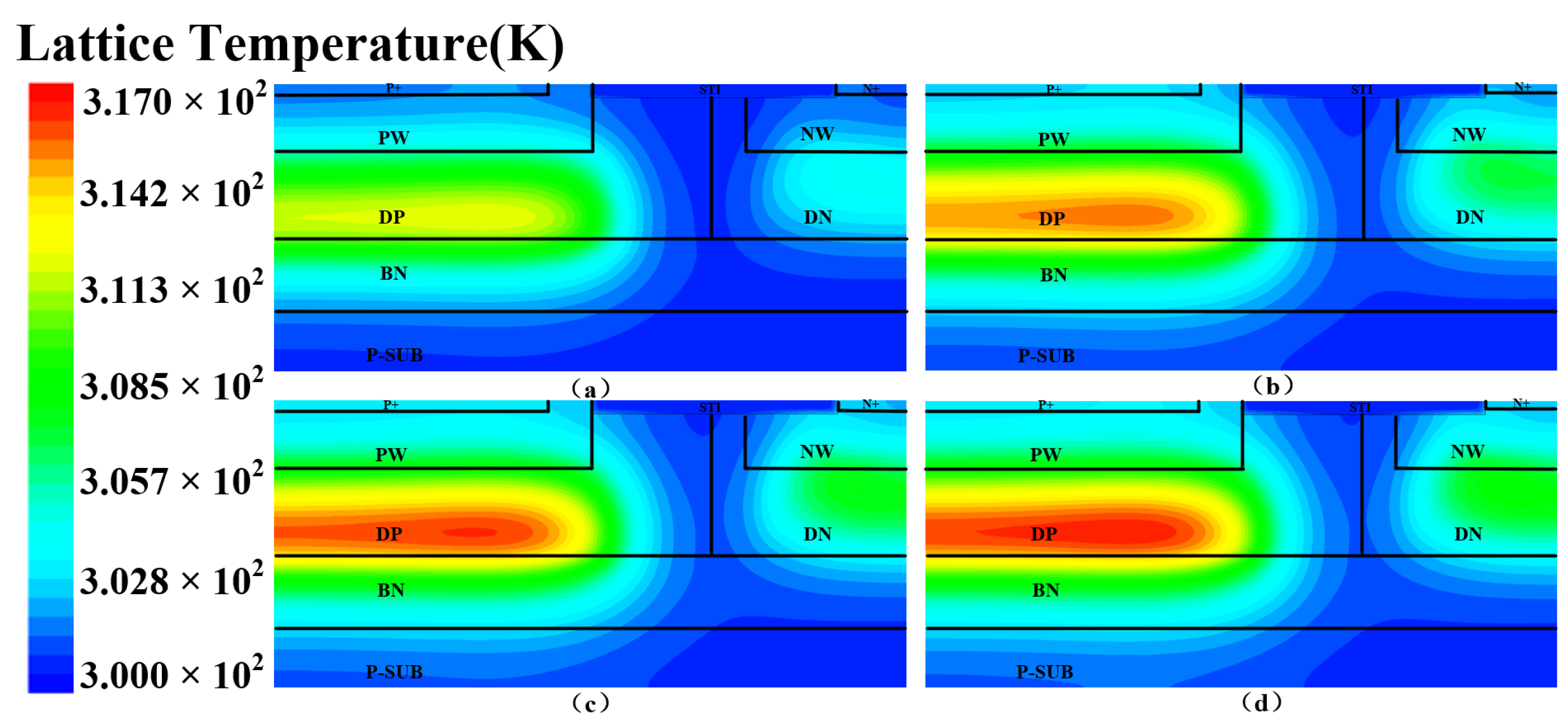
In this study, a self-heating model is established to characterize the influence of lattice temperature rise on the performance of single-photon avalanche diode devices, and an electro-thermal coupling model is proposed to describe the temperature distribution characteristics of SPADs during long-term operation under repeated avalanche-quenching cycles. As shown in Figure 3, with the avalanche time set to 2 ns and the quenching time set to 5 ns, TCAD simulation results indicate that the variation in the device’s lattice temperature is mainly concentrated in the vertical junction region, and the hot spot region exhibits a rounded rectangular shape. The simulation results in Figure 3a–d reveal the evolution law of the internal lattice temperature distribution of SPADs at different moments after avalanche, which provides an important theoretical basis for optimizing the device thermal management scheme and improving device reliability.
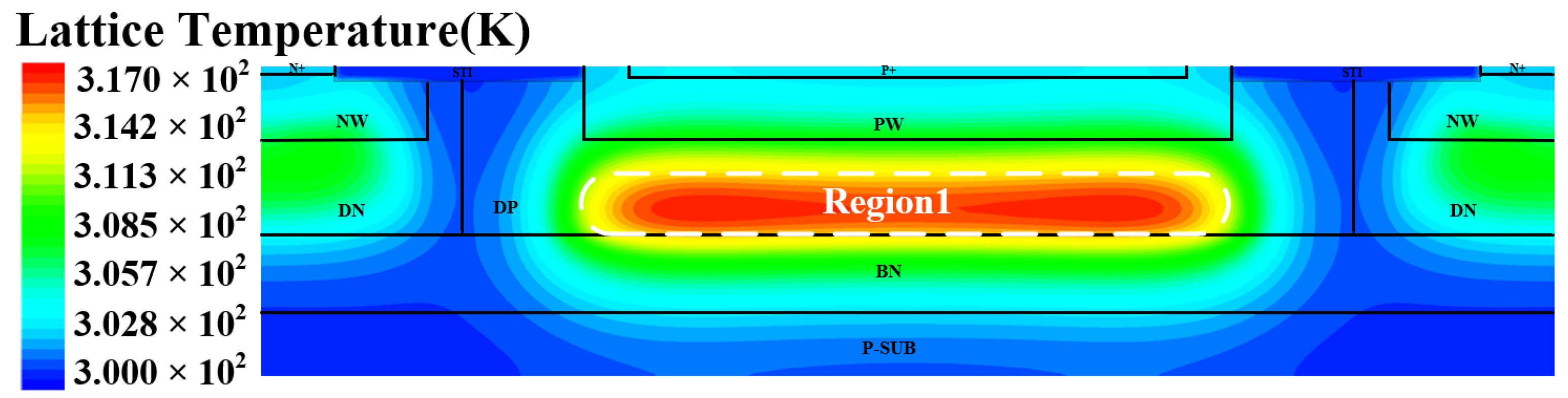
As shown in Figure 4, which presents the lattice temperature simulation results for the device at an operation time of 100 μs. The area enclosed by the white dashed line represents the hot spot region, defined as Region 1. Region 1 clearly corresponds to the core position of the vertical avalanche junction area of the device and serves as the central hot spot region with the peak temperature across the entire device structure. The high-temperature accumulation characteristic of this region originates from the intense impact ionization of carriers under the action of a high electric field during the avalanche process, where a large amount of kinetic energy is converted into lattice thermal energy. At the time node of 100 μs, however, the thermal energy has not been sufficiently diffused to the surrounding areas through thermal conduction, thus forming a localized high-temperature distribution in the junction area. The temperature amplitude of this region is significantly higher than that of other parts of the device, which directly reflects the physical characteristics of the junction area as the core of heat generation.
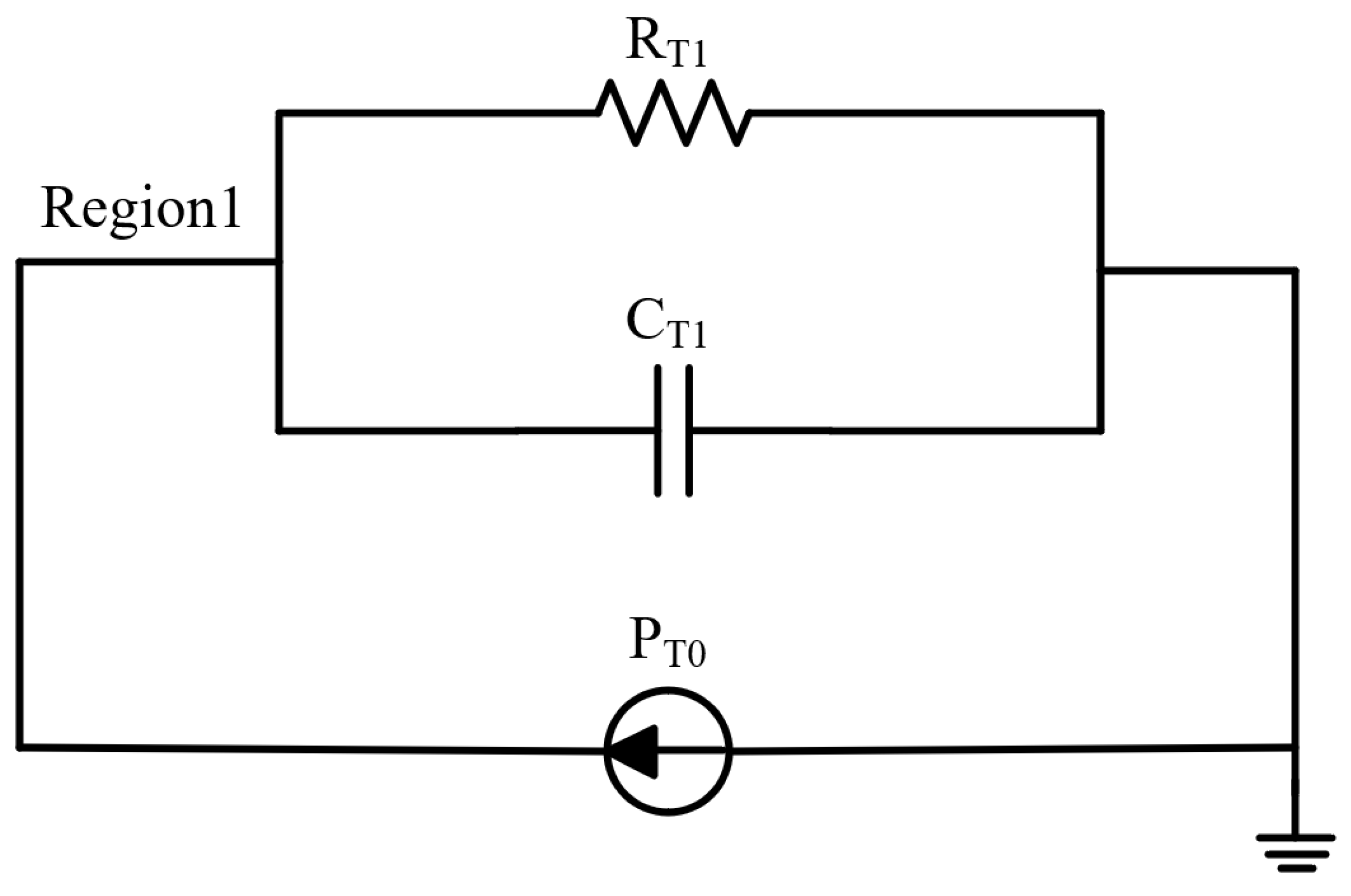
Figure 5 shows the Foster thermal model adopted in this study. Its component parameters, R T 1 and C T 1 , do not correspond to the actual distributed thermal resistance and thermal capacitance that physically exist inside the device but are derived through the parameter fitting method, P T 0 , which denotes the transient thermal input power applied to the device and serves as the excitation heat source for electro-thermal simulation. They are intended to accurately reproduce the overall transient temperature rise response curve of the device. The core function of this model is to provide the key junction center reference point lattice temperature for the temperature-dependent parameters in the SPAD model.
The values of equivalent thermal resistance, R T 1 , and thermal capacitance, C T 1 , in the Foster thermal resistance network can be obtained using the following formulas:
C T 1 = Q T = c t h · m = c t h · ρ · V t h e r m a l
where c t h is the specific heat capacity of the material, with the unit J · k g 1 · K 1 ; ρ is the material density; and V t h e r m a l is the effective thermal volume.
R T 1 = R D P + R D N + R B N + R s u b
where R D P denotes the thermal conduction resistance of the DP region, R D N that of the DN region, R B N that of the BN region, and R s u b that of the P-type substrate. Heat is primarily conducted from the avalanche junction region toward the DP, DN, BN, and substrate directions, and the total thermal resistance equals the sum of the thermal resistances of each layer. The fitted heat capacity and thermal resistance parameters are listed in Table 2.
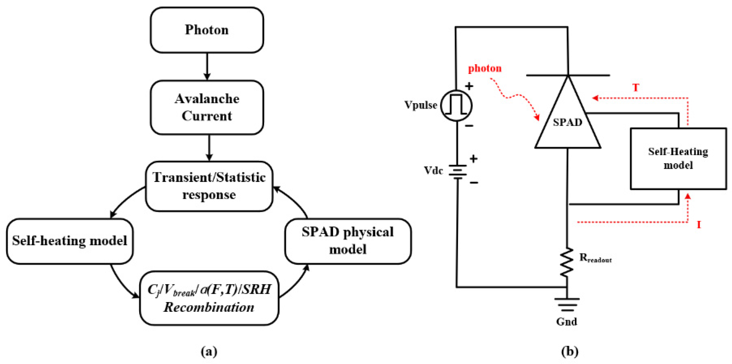
Figure 6a illustrates the working principle of the electro-thermal coupling model. When the SPAD absorbs photons, an avalanche current is generated, which serves as the input signal of the thermal model. After being processed by the heat capacity and thermal resistance modules, a voltage variation is output, which can be equivalent to the temperature variation of the device. The self-heating effect acts on key internal parameters of the device, including junction capacitance, breakdown voltage, ionization coefficient, and SRH recombination rate, and ultimately changes the transient and static characteristics of the SPAD. The variation in the avalanche current is then fed back to the self-heating model as the input, forming a closed-loop self-cycle. Figure 6b shows the circuit schematic of the model, in which gated quenching is adopted for device quenching. The operating mode is regulated by setting a voltage pulse: the device enters Geiger mode when the pulse is at a high level, and quenching is achieved when the pulse is at a low level.

3. Results and Discussion

3.1. Self-Heating Model Validation

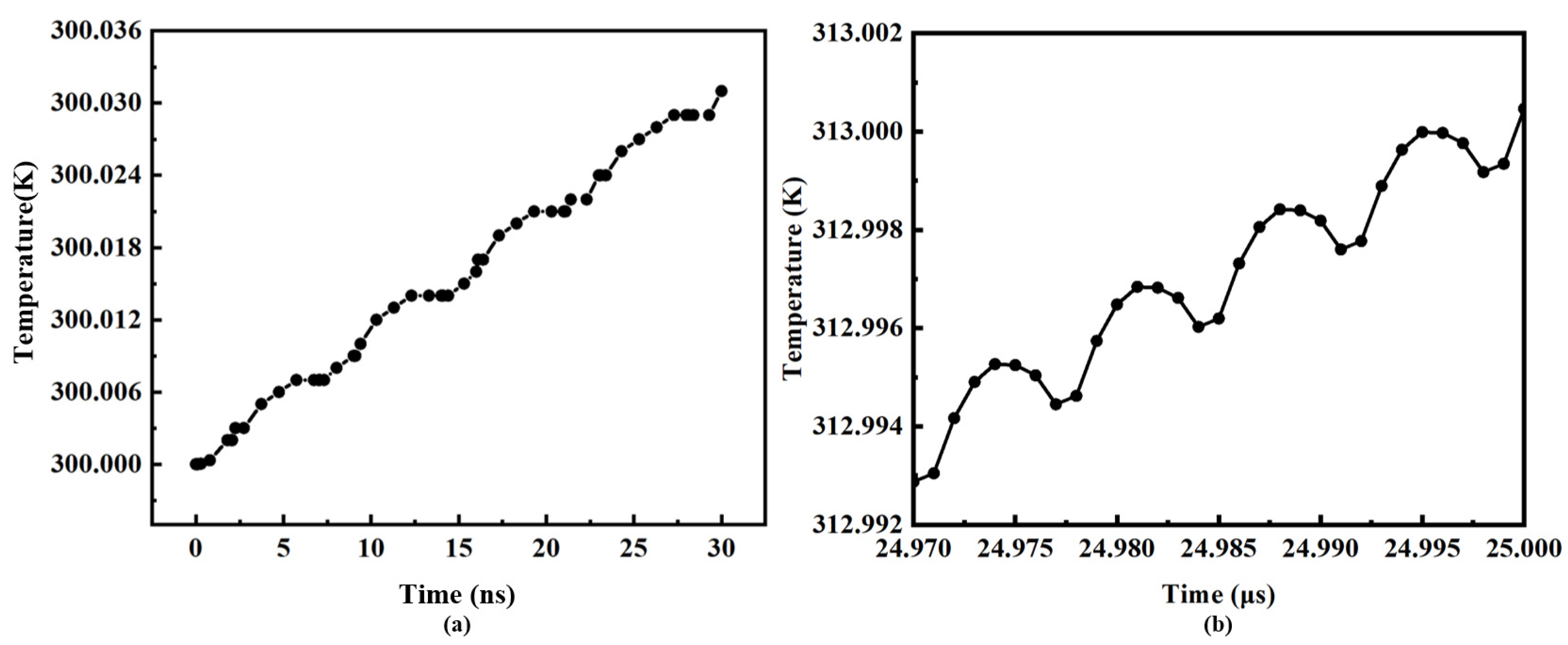
Based on the dynamic lattice temperature characteristics of the SPAD device obtained via TCAD simulations, the analysis of the temperature response behavior during the initial operation cycles reveals that the transient excitation of the avalanche current induces a rapid temperature rise in the device junction region. As shown in Figure 7a, a single avalanche event can cause an approximate temperature fluctuation of 0.08 K in the junction region; meanwhile, as the device current decays, the activation of the quenching effect further facilitates heat dissipation. Figure 7b presents the temperature variation around 25 μs, where it can be observed that the avalanche leads to a temperature rise of approximately 0.02 K, followed by a rapid temperature drop after quenching, with a significantly larger temperature reduction amplitude than that in Figure 7a. This phenomenon arises because the device exhibits a uniform overall temperature in the initial stage, resulting in a small temperature difference between the junction region and the environment, weak thermal driving force, and slow heat dissipation. In contrast, by 25 μs, the overall temperature of the device has increased, leading to a larger temperature difference between the peak junction temperature and the substrate/environment, a stronger thermal driving force, and thus a faster heat diffusion rate and a greater temperature fallback amplitude.
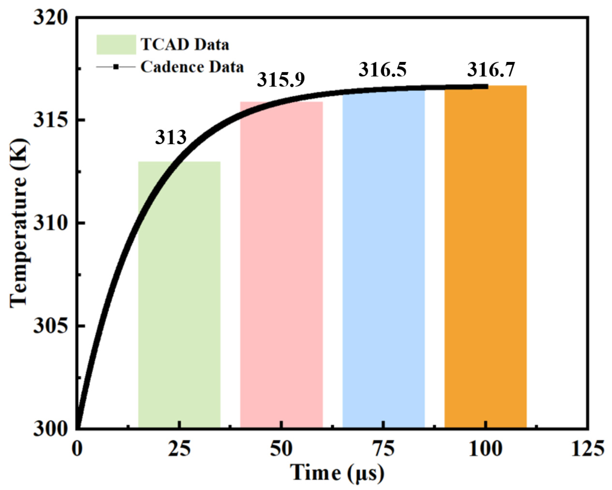
In this part, the circuit thermal model shown in Figure 5 is established using the Cadence simulation software, where the key parameters R T 1 and C T 1 are obtained by fitting with TCAD simulation data. With the SPAD avalanche current as the excitation source, the time-dependent variation in the lattice temperature in the junction region, as shown in Figure 8, can be obtained. In the bar chart of Figure 8, the green column indicates the lattice temperature of Region 1 at 25 μs obtained from TCAD simulation, which is 313 K. The pink, blue and orange columns correspond to the lattice temperatures at 50 μs, 75 μs and 100 μs, with values of 315.9 K, 316.5 K and 316.7 K respectively. The black curve in Figure 8 presents the simulation results of the Cadence circuit thermal model. The comparison shows that the lattice temperature calculated by the circuit thermal model is in good agreement with the TCAD simulation data.

3.2. SPAD Electro-Thermal Coupling Model Validation

3.2.1. SPAD Breakdown Voltage

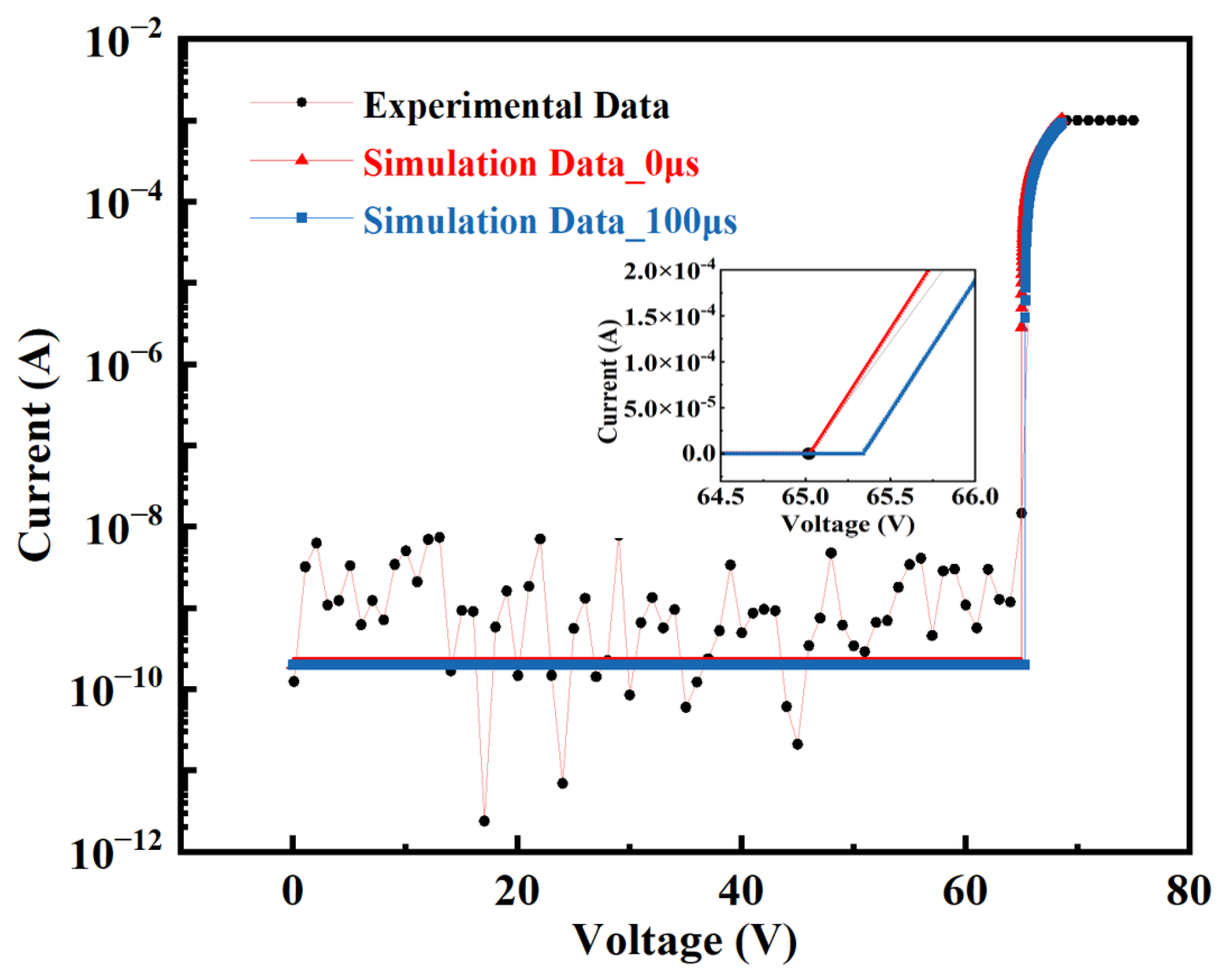
Figure 9 presents the simulation results of the breakdown voltage for the SPAD model. The black dotted line refers to experimental measurements, while the red and blue dotted lines denote the I–V curves at simulation durations of 0 μs and 100 μs, respectively. The simulated results exhibit great consistency with the measured data, which demonstrates the accuracy and rationality of the established electrothermal model.
Simulation results show that the breakdown voltage increases by approximately 0.34 V when the device operates for 100 μs. This increase in breakdown voltage leads to a decrease in the SPAD’s overbias voltage, which in turn affects key parameters such as PDP and DCR. In terms of PDP, if the overbias voltage decreases, the electric field strength in the junction area will weaken accordingly, and the acceleration energy obtained by carriers will decrease. This may cause weak photon signals that could originally trigger avalanches to ultimately fail to form effective avalanches, resulting in a decrease in PDP. In terms of the DCR, a decrease in overbias voltage weakens the electric field’s acceleration effect on noise carriers, resulting in a reduction in the number of noise carriers accelerated by the electric field.

3.2.2. SPAD Photon Detection Probability

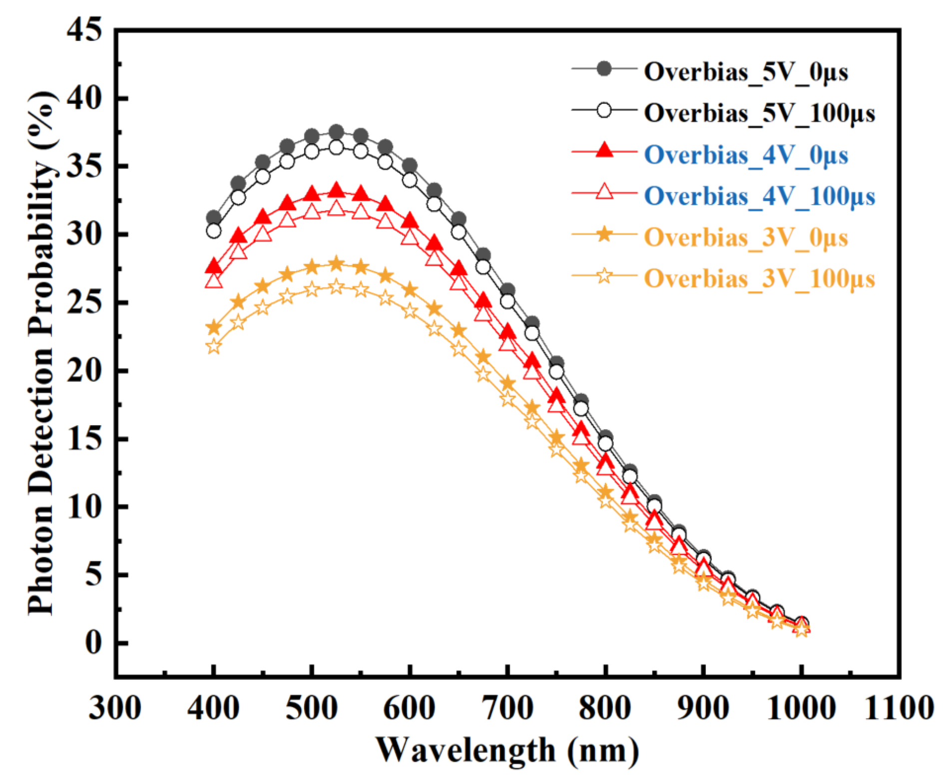
Figure 10 depicts the variation in the photon detection probability of the SPAD device with wavelength-under-overbias voltages of 3 V, 4 V, and 5 V. The simulation results demonstrate that the self-heating effect of the device significantly suppresses the PDP. Specifically, under the 5 V overbias voltage, the peak PDP decreases from the initial 37.52% to 36.39%; under the 4 V overbias voltage, the peak PDP decreases from 33.13% to 31.80%; and under the 3 V overbias voltage, the peak PDP decreases from 27.83% to 26.16%. It is worth noting that the self-heating effect leads to a considerable reduction in the PDP under the 3 V overbias voltage, with a peak PDP drop of 1.67%, whereas the peak PDP drop caused by the self-heating effect under the 5 V overbias voltage is 1.13%. Therefore, increasing the overbias voltage can effectively reduce the sensitivity of the device’s PDP to temperature variations.

3.2.3. SPAD Dark Count Rate

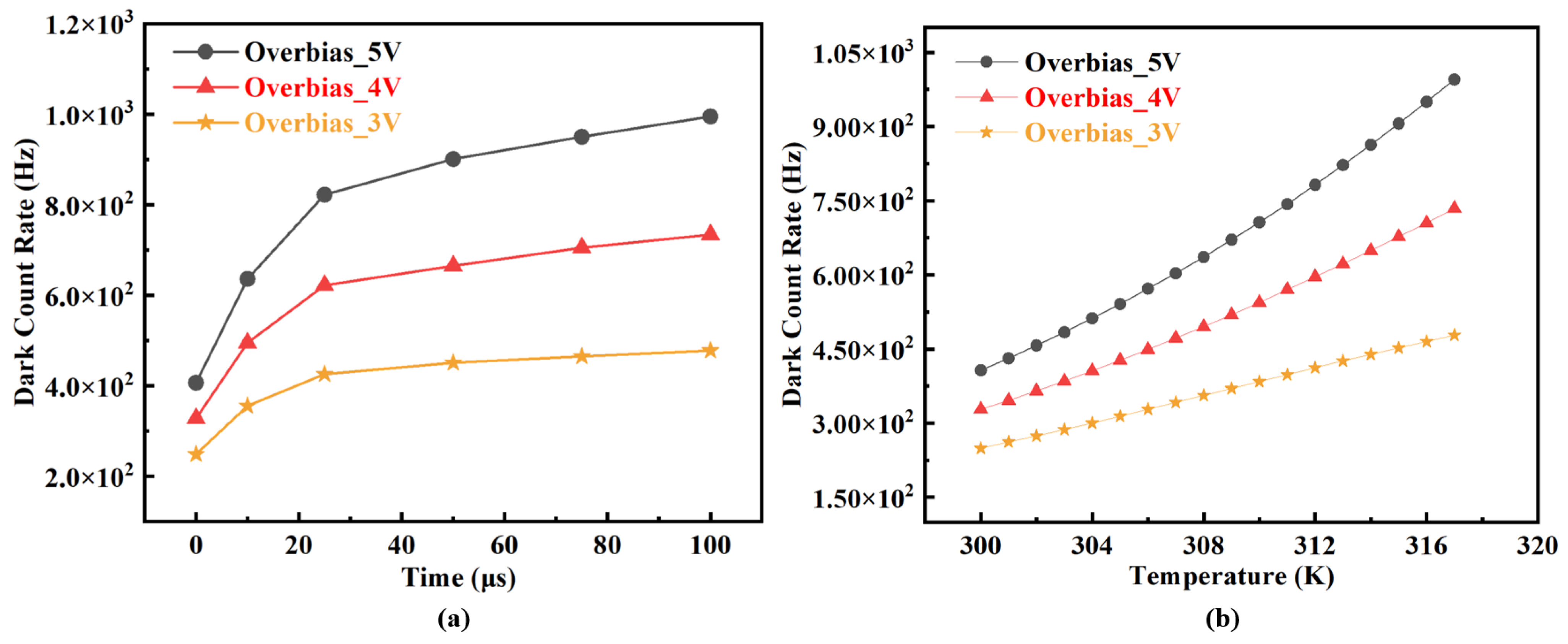
As the SPAD undergoes repeated avalanche-quenching cycles, significant heat gradually accumulates in its junction region, exciting more thermal carriers and thus causing the device’s dark count rate to increase continuously with operating time, as shown in Figure 11a. Under 5 V overbias voltage, the dark count rate rises from 407 Hz to 995 Hz after 100 μs; under 4 V, it increases from 338 Hz to 734 Hz; and under 3 V, it goes up from 249 Hz to 478 Hz. To further investigate the regulatory mechanism of junction temperature variation induced by self-heating effects on the dark count rate under different operating durations, Figure 11b shows that the dark count rate increases exponentially with temperature under 5 V overbias voltage, while the exponential characteristic of the dark count rate with increasing temperature approaches linearity under 3 V overbias voltage. The physical mechanism is that at low overbias voltage, increased junction lattice temperature raises the breakdown voltage, reducing the effective overbias voltage and avalanche probability and weakening thermal carriers induced avalanches. The growing number of thermal carriers with temperature ultimately leads to an overall increase in dark count rate. Therefore, the SPAD model with self-heating coupling better conforms to realistic working conditions. This electro-thermal SPAD model provides a fundamental tool for the design and optimization of peripheral circuits to reduce the dark count rate.

3.2.4. SPAD Transient Characteristic Verification

This study mainly focuses on the influence of the junction center hot spot area on device performance and integrates the electrical model with the self-heating model to establish an electro-thermal coupling model. Considering the complexity of the potential in the junction capacitance and potential numerical convergence issues, this model ignores the influence of the built-in potential on the capacitance. Therefore, the SPAD capacitance formula is simplified as
C j = C j 0 · [ 1 + m · ( A c · ( T T 0 ) ) ]
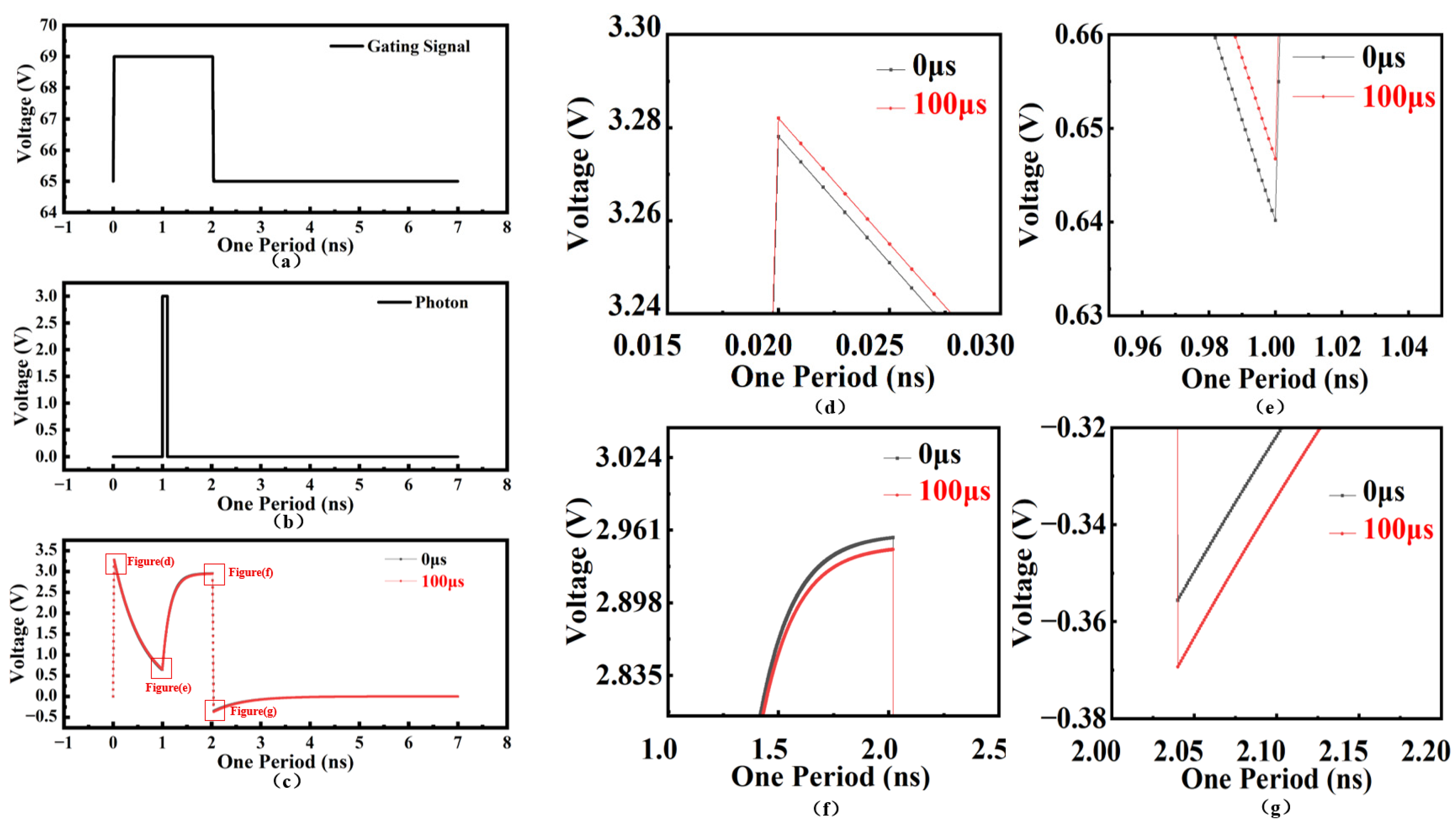
Figure 12 presents the transient characteristic data of the SPAD within a single operating cycle under the simulation conditions of pulsed photon incidence, 4 V overbias voltage, and 10 kΩ readout resistor R r e a d o u t . Among them, Figure 12a shows the gated signal waveform, Figure 12b depicts the incident photon pulse waveform, Figure 12c illustrates the voltage waveform across the readout resistor, and Figure 12d–g display the locally amplified views of the voltage waveform at different stages in Figure 12c. It can be seen from Figure 12d that when the gated signal switches from the low potential to the high potential, the self-heating effect significantly increases the voltage peak across the readout resistor. The underlying mechanism is that the self-heating effect leads to an increase in device capacitance, which in turn enhances the response current, I t r a n , at the moment of gated signal transition. The variation law of this current can be derived from Equation (23), where V t r a n represents the instantaneous voltage. This increase in current further causes a synchronous rise in the voltage across the readout resistor after the SPAD receives photons, as shown in Figure 12e.
I t r a n = C j · d V t r a n d t
Figure 12f displays the signal waveform of the SPAD after photon absorption and avalanche breakdown. It can be observed that the capacitance variation induced by the self-heating effect reduces the readout signal voltage by approximately 0.01 V. This is because the self-heating effect alters the breakdown voltage of the device, leading to a decrease in the overbias voltage, which in turn weakens the avalanche current of the SPAD and ultimately results in a voltage drop across the readout resistor. Notably, after this voltage drop is processed by the subsequent amplification circuit, the negative impact of the self-heating effect will be further amplified, thus degrading the detection accuracy of the system. In Figure 12g, the self-heating effect increases the junction capacitance of the device, thereby increasing the amount of stored charge accordingly. Therefore, when the gated signal switches from high potential to low potential, a higher peak voltage appears across the readout resistor, and the time required for charge release is also prolonged.
The negative spike across the readout resistor in Figure 12g reflects the voltage variation during SPAD quenching and recovery. The negative falling edge and subsequent voltage restoration of the avalanche signal correspond to junction charge dissipation and electric field reconstruction after avalanche quenching, and this whole relaxation process is defined as the intrinsic recovery behavior of the SPAD. During this period, the SPAD cannot maintain Geiger-mode operation. The device total dead time covers two sequential stages: the avalanche duration and the intrinsic recovery time. Therefore, the intrinsic recovery time is an essential part of the dead time under the gated operation scheme.
The intrinsic recovery time, τ r e t , is uniformly defined as the time interval from the peak of the quenched avalanche pulse to the complete stabilization of device voltage and electric field, which is a core component determining the total dead time. The overall device dead time refers to the total period from avalanche triggering to the full restoration of the SPAD for detecting subsequent single photons. It is co-determined by the avalanche sustaining duration and the intrinsic recovery time, and fundamentally restricts the maximum photon counting rate and time resolution of the SPAD.
The variation in junction capacitance induced by the self-heating effect greatly affects the recovery time of the SPAD. An extended recovery time will restrict the maximum photon counting capability. Especially under high-frequency photon incidence, excessive dead time will lead to the loss of subsequent photon signals, reduce photon counting accuracy, and further degrade the detection performance of LiDAR for high-speed moving targets.
To quantitatively analyze the self-heating effect on recovery time and further clarify its impact on total device dead time, the intrinsic recovery time can be calculated by Equation (24) [24]:
τ r e t ( C j + C s ) · R r e a d o u t
where C s is defined as the stray capacitance existing between the device anode and cathode. Consequently, the quantitative expression for temperature-induced recovery time drift is derived as
τ r e t C · R r e a d o u t
The calculation results demonstrate that the overall dead time of the SPAD device increases by 3.34 ps due to the recovery time drift induced by self-heating. Benefiting from the low junction capacitance of the single-pixel device in this work, the influence of self-heating on individual-pixel timing performance is relatively weak. However, for large-scale SPAD arrays, the parallel pixel layout greatly raises the equivalent total capacitance. In this case, self-heating will obviously prolong the recovery time and further deteriorate the dead-time characteristic of the array. Therefore, investigating the mechanism of the self-heating effect on SPAD devices is essential for the design and performance optimization of SPAD arrays in further research.

4. Conclusions

This study proposes an integrated electro-thermal coupling model for SPAD devices that characterizes the transient evolution of lattice temperature during the avalanche process through a thermal network and quantifies the temperature dependence of key physical parameters, including junction capacitance, breakdown voltage, impact ionization coefficients and SRH recombination rates. The quenching circuit adopted in this paper is an idealized model, where the thermal contribution from the quenching circuit is neglected, aiming to investigate the impact of the device’s intrinsic heat generation. The simulation results show that after 100 μs of operation, the temperature rise caused by avalanche increases the device dead time by approximately 3.34 ps and reduces the detection accuracy of LiDAR. Meanwhile, the self-heating effect leads to a 0.34 V shift in the SPAD breakdown voltage, which significantly degrades the device performance. Specifically, the photon detection probability drops by 1.13% at 5 V overbias voltage, and the reduction rises to 1.67% when the overbias voltage decreases to 3 V, indicating that a lower overbias voltage aggravates the degradation of photon detection probability induced by self-heating. Further dark count rate simulations reveal that the rise of junction lattice temperature increases the device breakdown voltage, which reduces the actual effective overbias voltage and avalanche probability, thus weakening the avalanche probability triggered by thermal carriers. Nevertheless, the number of thermal carriers keeps growing with the increase of junction temperature, resulting in an overall rise of the dark count rate contributed by thermal carriers and an upward trend of the total dark count rate. In summary, this study successfully establishes an electro-thermal coupling model for SPAD devices. The model can effectively describe the performance variations caused by the change of junction lattice temperature after long-term avalanche, accurately predict the practical operating characteristics of the device, and provide important technical support for the industrial development of solid-state LiDAR.

Author Contributions

Conceptualization, C.W.; methodology, C.W.; software, C.W.; validation, C.W.; formal analysis, C.W.; investigation, J.L.; resources, J.L.; data curation, C.W.; writing—original draft preparation, C.W.; writing—review and editing, Z.Z. and W.L.; visualization, C.W.; supervision, J.L.; project administration, J.L.; funding acquisition, J.L. All authors have read and agreed to the published version of the manuscript.

Funding

This work was supported by the Fundamental Research Funds for the Central Universities (JUSRP123062) and the Natural Science Foundation of Jiangsu Province of China (BK20231038).

Data Availability Statement

The data is unavailable due to privacy and ethical restrictions.

Acknowledgments

We gratefully acknowledge the financial support from the Fundamental Research Funds for the Central Universities (Grant No. JUSRP123062) and the Natural Science Foundation of Jiangsu Province of China (Grant No. BK20231038).

Conflicts of Interest

The authors declare no conflicts of interest.

Abbreviations

The following abbreviations are used in this manuscript:
SPADSingle-Photon Avalanche Diode
PDPPhoton Detection Probability
DCRDark Count Rate
SRHShockley–Read–Hall
ESDElectrostatic Discharge
TCADTechnology Computer-Aided Design
BCDBipolar-CMOS-DMOS
SPICESimulation Program with Integrated Circuit Emphasis

References

  1. Albert, K.; Ligges, M.; Henschke, A.; Ruskowski, J.; De Zoysa, M.; Noda, S.; Grabmaier, A. Performance Comparison of Multipixel Biaxial Scanning Direct Time-of-Flight Light Detection and Ranging Systems with and Without Imaging Optics. Sensors 2025, 25, 3229. [Google Scholar] [CrossRef] [PubMed]
  2. Villa, F.; Severini, F.; Madonini, F.; Zappa, F. SPADs and SiPMs Arrays for Long-Range High-Speed Light Detection and Ranging (LiDAR). Sensors 2021, 21, 3839. [Google Scholar] [CrossRef] [PubMed]
  3. Beer, M.; Haase, J.F.; Ruskowski, J.; Kokozinski, R. Background Light Rejection in SPAD-Based LiDAR Sensors by Adaptive Photon Coincidence Detection. Sensors 2018, 18, 4338. [Google Scholar] [CrossRef] [PubMed]
  4. Chen, M.; Rao, P.R.; Venialgo, E. Depth estimation in SPAD-based LIDAR sensors. Opt. Express 2024, 32, 3006. [Google Scholar] [CrossRef] [PubMed]
  5. Dalla Mora, A.; Tosi, A.; Tisa, S.; Zappa, F. Single-Photon Avalanche Diode Model for Circuit Simulations. IEEE Photon. Technol. Lett. 2007, 19, 1922–1924. [Google Scholar] [CrossRef]
  6. Zappa, F.; Tosi, A.; Mora, A.D.; Tisa, S. SPICE modeling of single photon avalanche diodes. Sens. Actuators A Phys. 2009, 153, 197–204. [Google Scholar] [CrossRef]
  7. Mita, R.; Palumbo, G.; Fallica, P.G. Accurate model for single-photon avalanche diodes. IET Circuits Devices Syst. 2008, 2, 207–212. [Google Scholar] [CrossRef]
  8. He, Q.; Xu, Y.; Zhao, F. An accurate simulation model for single-photon avalanche diodes including important statistical effects. J. Semicond. 2013, 34, 104007. [Google Scholar] [CrossRef]
  9. Giustolisi, G.; Mita, R.; Palumbo, G. Behavioral modeling of statistical phenomena of single-photon avalanche diodes. Circuit Theory Apps 2012, 40, 661–679. [Google Scholar] [CrossRef]
  10. Maciazek, P.; Nicholson, I.; Manouvrier, J.; Rideau, D.; Kaklin, F.; Lacombe, E.; Al–Rawhani, M.; Bu, C.; Pellegrini, S.; Georgiev, V. Automated Algorithmic Parameter Extraction of TCAD-Based SPAD SPICE Models. In Proceedings of the 2024 International Conference on Simulation of Semiconductor Processes and Devices (SISPAD); IEEE: San Jose, CA, USA, 2024; pp. 1–4. [Google Scholar]
  11. Klauner, T.; Alirezaei, I.S.; Roisin, N.; André, N.; Flandre, D. SPICE Model of SPAD Transient Intrinsic Response Validated using Mixed-Mode TCAD Simulations. In Proceedings of the ESSDERC 2023—IEEE 53rd European Solid-State Device Research Conference (ESSDERC); IEEE: Lisbon, Portugal, 2023; pp. 136–139. [Google Scholar]
  12. El-Dakroury, M.M.; Eladawy, M.I.; Nosseir, Z.B.; Ismail, Y.; Abdelhamid, H. Modeling of Double-gate LDMOSFET Devices including Self-heating. In Proceedings of the 2019 31st International Conference on Microelectronics (ICM); IEEE: Cairo, Egypt, 2019; pp. 235–239. [Google Scholar]
  13. Pan, Z.; Li, C.; Di, M.; Zhang, F.; Wang, A. 3D TCAD Analysis Enabling ESD Layout Design Optimization. IEEE J. Electron Devices Soc. 2020, 8, 1289–1296. [Google Scholar] [CrossRef]
  14. Wang, H.; Liang, H.; Liu, J. A Compact Model with Self-Heating Effect Applying to the SCR Device for ESD Protection. Electronics 2025, 14, 843. [Google Scholar] [CrossRef]
  15. Chen, X.; Chen, Y.; Liu, J.; Ren, M. PN junction. In Microelectronic Devices, 4th ed.; Publishing House of Electronics Industry: Beijing, China, 2018; pp. 74–76. [Google Scholar]
  16. Vecchi, M.C.; Rudan, M. Modeling electron and hole transport with full-band structure effects by means of the Spherical-Harmonics Expansion of the BTE. IEEE Trans. Electron Devices 1998, 45, 230–238. [Google Scholar] [CrossRef]
  17. Panglosse, A.; Martin-Gonthier, P.; Marcelot, O.; Virmontois, C.; Saint-Pé, O.; Magnan, P. Modeling, simulation methods and characterization of photon detection probability in CMOS-SPAD. Sensors 2021, 21, 5860. [Google Scholar] [CrossRef] [PubMed]
  18. Miah, M.A.R.; Islam, M.S.; Alam, M.S. Simulation and modeling of single photon avalanche diodes. Int. J. High Speed Electron. Syst. 2015, 24, 1520006. [Google Scholar]
  19. Hofbauer, M.; Steindl, B.; Zimmermann, H. Temperature Dependence of Dark Count Rate and After Pulsing of a Single-Photon Avalanche Diode with an Integrated Active Quenching Circuit in 0.35 μm CMOS. J. Sens. 2018, 2018, 9585931. [Google Scholar] [CrossRef]
  20. Shockley, W.; Read, W.T. Statistics of the Recombinations of Holes and Electrons. Phys. Rev. 1952, 87, 835–842. [Google Scholar] [CrossRef]
  21. Wachutka, G. An Extended Thermodynamic Model for the Simultaneous Simulation of the Thermal and Electrical Behaviour of Semiconductor Devices. In Proceedings of the Sixth International Conference on the Numerical Analysis of Semiconductor Devices and Integrated Circuits (NASECODE VI), Dublin, Ireland, 11–14 July 1989; pp. 409–414. [Google Scholar]
  22. Callen, H.B. Thermodynamics and an Introduction to Thermostatistics, 2nd ed.; John Wiley & Sons: New York, NY, USA, 1985. [Google Scholar]
  23. Shanks, H.R.; Maycock, P.D.; Sidles, P.H.; Danielson, G.C. Thermal Conductivity of Silicon from 300 to 1400 K. Phys. Rev. 1963, 130, 1743–1748. [Google Scholar] [CrossRef]
  24. Tisa, S.; Zappa, F.; Tosi, A.; Cova, S. Electronics for single photon avalanche diode arrays. Sens. Actuators A Phys. 2007, 140, 113–122. [Google Scholar] [CrossRef]
Figure 1. SPAD equivalent circuit diagram.
Inventions 11 00045 g001
Figure 2. Charge transport relationship at PN junction equilibrium.
Inventions 11 00045 g002
Figure 3. Simulation of SPAD lattice temperature in (a) at 25 μs; (b) at 50 μs; (c) at 75 μs; (d) at 100 μs.
Inventions 11 00045 g003
Figure 4. Diagram of lattice temperature region division at 100 μs.
Inventions 11 00045 g004
Figure 5. Foster thermal model.
Inventions 11 00045 g005
Figure 6. (a) SPAD self-heating model flowchart; (b) test diagram of SPAD.
Inventions 11 00045 g006
Figure 7. Variations in lattice temperature at different time intervals. (a) 0–30 ns; (b) 24.97–25 μs.
Inventions 11 00045 g007
Figure 8. Self-heating model simulation.
Inventions 11 00045 g008
Figure 9. SPAD static I-V curve.
Inventions 11 00045 g009
Figure 10. Simulation curve of PDP with self-heating effects.
Inventions 11 00045 g010
Figure 11. (a) Curves of relationship between overbias voltages and DCR at different times; (b) curves of relationship between temperature and DCR under different overbias voltages.
Inventions 11 00045 g011
Figure 12. Transient simulation of SPAD: (a) gating signal pulse; (b) voltage pulse of simulated photons; (c) voltage waveform across the readout resistor; (dg) staged partial enlarged views of the voltage waveform across the readout resistor.
Inventions 11 00045 g012
Table 1. Reference values of parameters for the model.
ParametersValues
R b r e a k   [ Ω ] 3500
I s   [ A ] 2 × 10 10
T 0   [ K ] 300
C j 0 [fF]50
C a / C c [fF]10
ε 0   [ F / m ] 8.854 × 10 12
ε r   [ F / m ] 11.7
q   [ C ] 1.602 × 10 19
k B   [ J / K ] 1.38 × 10 23
A   [ c m 3 K 3 / 2 ] 1.3 × 10 16
E g ( 0 )   [ e V ] 1.17
m 1
A c 4.0 × 10 4
α S i 4.73 × 10 4
β S i 636
V n 0.01
Table 2. Thermal network fitting parameters.
ParametersValues
C T 1   [ n F ] 0.287
R T 1   [ k Ω ] 57.7
Disclaimer/Publisher’s Note: The statements, opinions and data contained in all publications are solely those of the individual author(s) and contributor(s) and not of MDPI and/or the editor(s). MDPI and/or the editor(s) disclaim responsibility for any injury to people or property resulting from any ideas, methods, instructions or products referred to in the content.