Review

Recent Advances in Aluminum Nitride (AlN) Growth by Magnetron Sputtering Techniques and Its Applications

by
Nabeel Ahmad Khan Jadoon
,
Vaigunthan Puvanenthiram
,
Mayada Ahmed Hassan Mosa
,
Ashutosh Sharma
and
Kaiying Wang
*
Department of Microsystems, University of South-Eastern Norway, 3184 Horten, Norway
*
Author to whom correspondence should be addressed.
Inorganics 2024, 12(10), 264; https://doi.org/10.3390/inorganics12100264
Submission received: 29 August 2024 / Revised: 30 September 2024 / Accepted: 4 October 2024 / Published: 7 October 2024
(This article belongs to the Special Issue Advanced Inorganic Semiconductor Materials, 2nd Edition)

Abstract

:
This review explores the processes involved in enhancing AlN film quality through various magnetron sputtering techniques, crucial for optimizing performance and expanding their application scope. It presents recent advancements in growing AlN thin films via magnetron sputtering, elucidating the mechanisms of AlN growth and navigating the complexities of thin-film fabrication. Emphasis is placed on different sputtering methods such as DC, RF, pulsed DC, and high-power impulse DC, highlighting how tailored sputtering conditions enhance film characteristics in each method. Additionally, the review discusses recent research findings showcasing the dynamic potential of these techniques. The practical applications of AlN thin films, including wave resonators, energy harvesting devices, and thermal management solutions, are outlined, demonstrating their relevance in addressing real-world engineering challenges.

1. Introduction

Aluminum nitride (AlN)-based thin films have gained significant attention due to their unique physicochemical characteristics [1], including high piezoelectricity [2,3,4], substantial surface acoustic velocity [5,6,7,8], electromechanical coupling [9], chemical stability, and broad transparency across various spectral ranges [10,11,12]. In addition to AlN, other materials such as GaN and InN are significant within the III-nitride family. GaN is particularly well-known for its excellent thermal stability, and ability to emit light across both the visible and ultraviolet spectrum [13]. While GaN is typically grown using techniques like molecular beam epitaxy (MBE) or metal–organic chemical vapor deposition (MOCVD), sputtering presents a more cost-effective alternative, making it an attractive option for certain applications [14]. Furqan et al. have demonstrated that the thin-film growth of GaN with magnetron sputtering creates growth along the (002) plane, as well as demonstrating the effects of growth parameters on the quality of films [15].
Another material, like indium nitride (InN), characterized by Faiza et al., showed excellent growth in the c-plane and related to film hexagonal material properties like electrical resistivity, which is decreased when increasing the power in the process of DC magnetron sputtering [16]. Zinc oxide (ZnO), a hexagonal material known for its high Seebeck coefficient and transparent thermoelectric performance, is suitable for thermoelectric and optoelectronic applications [17]. Among various deposition methods available for synthesizing ZnO films, magnetron sputtering stands out for its ability to maintain precise control over growth conditions, leading to the facilitation of the production of c-axis-oriented ZnO films with reproducible and controllable properties [18]. Although several options can be explored, the focus of this review is to explore AlN for magnetron sputtering.
Achieving the optimal performance of AlN films heavily depends on the methods used for their deposition. The deposition techniques play a critical role in producing AlN films with the desired quality and preferred orientations, which directly impact their effectiveness and functionality in specific technological contexts. The deposition methods include molecular beam epitaxy [19,20], magnetron sputtering [21], and chemical vapor deposition [22,23]. Among these techniques, magnetron sputtering stands out due to its superior parameter control, low-temperature operation, and compatibility with semiconductor technology. For example, studies [24,25,26] have shown that magnetron sputtering allows for precise control over film thickness and composition, which is crucial for applications requiring high precision.
The utilization of magnetron sputtering has showcased significant progress in maximizing the yield and quality of AlN films. For instance, Barth [24] highlighted the potential of scandium doping in AlN films by pulse magnetron sputtering to enhance energy harvesting capabilities, while Jiang [27] proposed a deposition using middle-frequency magnetron sputtering yielding highly c-axis-oriented AlN films on titanium alloy substrate, particularly suited for piezoelectric MEMS and SAW devices [25]. Additionally, Uchiyama [28] achieved uniform and smooth AlN films on sapphire substrates by RF magnetron sputtering, and Ke et al. [29] enhanced the deposition rate of highly c-axis-oriented AlN films using unbalanced magnetron sputtering. This method involves the use of an asymmetrical magnetic field configuration to increase plasma density near the target, resulting in denser grains and reduced surface roughness. Unlike conventional magnetron sputtering, unbalanced magnetron sputtering enhances ion bombardment and increases plasma density at the substrate surface, thereby resulting in improved film properties such as higher density and better crystalline quality, which are critical for high-performance electronic and optical devices.
While magnetron sputtering is acknowledged as an effective technique for AlN growth, it presents several challenges, such as predicting thin-film structures amidst fluctuating sputter parameters [20]. Additionally, the meticulous management of crystallinity, thickness consistency, and stress levels is required to meet the demands of high-volume manufacturing. The formation of the transparent AlN phase is susceptible to variations in reactant gases like nitrogen (N2) and the flow rates during sputtering procedures [26]. Achieving superior quality AlN films necessitates adherence to specific processing prerequisites, such as an optimized nitrogen and argon ratio (N2/Ar) and reduced pressure during growth [30]. Furthermore, depositing AlN onto diverse substrates can induce divergent stress states within the film, influencing its inherent properties [31]. These challenges underscore the importance of precise control and optimization in the magnetron sputtering processes for the successful fabrication of high-quality AlN films. One significant challenge is the incorporation of oxygen in vacuum systems, which can adversely affect the crystallinity and properties of the films. Magnetron sputtering, particularly RF magnetron sputtering, mitigates oxygen incorporation by enabling precise control over sputtering parameters, thus ensuring the growth of high-quality crystalline AlN films, as demonstrated by studies such as [32] using radio frequency (RF) magnetron sputtering. Through meticulous parameter control—including adjusting the N2/Ar gas flow ratio, sputtering power, substrate temperature, and deposition pressure—researchers achieved high-quality films with optimal stoichiometry and minimal oxygen content. Control was attained by precisely regulating gas flow rates, maintaining substrate temperatures within an optimal range of 200–500 °C, and fine-tuning sputtering power and deposition pressure. This comprehensive approach underscores the effectiveness of magnetron sputtering in addressing oxygen incorporation challenges and ensuring the fabrication of crystalline AlN films with the desired properties.
Apart from the need for optimizing operational parameters in magnetron sputtering, achieving desired orientation growth in the (100), (110), or (001) planes is critically dependent on the specific methods used within the magnetron sputtering domain. Investigating parameters related to the type of magnetron sputtering method is essential, and a combined discussion of these methods for AlN growth has not been explored in previous reviews. Therefore, this review aims to provide a comprehensive understanding of the sequential growth of AlN films in light of recent advances in magnetron sputtering. Additionally, we examine how different magnetron sputtering methods influence AlN film fabrication and application, focusing on sputtering conditions and parameter controls.
Although several parameters are essential for the control of the thin-film growth of AlN, some superior parameter control in magnetron sputtering involves the precise adjustment of several key deposition parameters, such as gas flow ratios (N2/Ar), sputtering power, substrate temperature, deposition pressure, and ion bombardment control through magnetic field adjustments. These parameters are crucial for optimizing aluminum nitride (AlN) film quality. For instance, the N2/Ar ratio influences the film’s stoichiometry and properties, while sputtering power affects the energy of the sputtered atoms and the deposition rate. Maintaining an optimal substrate temperature, typically between 200–500 °C, enhances atom mobility and promotes desirable crystalline structures. Additionally, controlling the deposition pressure allows for better management of the mean free path of the sputtered particles, essential for achieving uniform film growth. Finally, regulating ion bombardment through magnetic field configuration significantly impacts film density and crystalline quality. Together, these factors facilitate the fabrication of high-quality AlN films with tailored properties for various applications.
The paper is structured as follows: The section on AlN growth describes the growth mechanisms, focusing on the desired crystallographic growth of aluminum nitride (AlN) and offering a comprehensive overview of the process. This foundational understanding is essential as it sets the stage for the subsequent sections. Given that the growth mechanism necessitates various fabrication methods through magnetron sputtering, the Fabrication section delves into these requirements, detailing the system architecture involved in magnetron chambers. It emphasizes the significance of different sputtering techniques, thoroughly analyzing their contributions and ultimately recommending the most suitable methods for specific applications within the magnetron sputtering domain. This section also discusses the doping mechanisms for AlN with other materials, highlighting how these modifications can enhance the material’s properties. Furthermore, the final section introduces the applications of AlN-based products. The schematic depiction in Figure 1 encapsulates the sequential progression inherent in developing and deploying AlN-based sensors, commencing from the foundational magnetron sputtering process and extending to their varied applications across diverse fields.

2. AlN Growth and Mechanism

2.1. AlN Crystal Structure and Growth Mechanism

The orientation of aluminium nitride (AlN) growth on a substrate is determined by which plane of the AlN unit cell becomes parallel to the substrate surface. The covalent bonds between aluminium (Al) and nitrogen (N) atoms form a triangular prism base, resulting in different lattice parameter values. An illustration of the lattice structure with these parameter values is depicted in Figure 2b, while the AlN unit cell, forming a hexagonal wurtzite structure, is shown in Figure 2a. Detailed studies have shown that substrate temperature and sputtering power significantly affect this orientation, highlighting the importance of precise control over these parameters [1].
The potential crystal orientations for AlN film growth primarily include the AlN(100) and AlN(001) planes. The preferred orientation is determined by the ratio of energy absorbed by the two vibrational phonon modes. The c-axis lies in the (100) plane, while the a-axis is parallel to the (001) plane. Detailed studies have shown that when the target-to-substrate distance is significantly larger than the mean free path, the AlN(100) orientation is favored due to lower energy atoms. In contrast, high-energy nitrogen and aluminium species, with a considerable mean free path relative to the target–substrate distance, favor the AlN(001) orientation. The mean free path during AlN growth is influenced by the working pressure, affecting the c-axis orientation of the deposited films. At higher working pressures, the mean free path of the sputtered species is reduced, resulting in lower-energy atoms reaching the substrate and favoring the AlN(100) orientation. Conversely, at lower working pressures, the mean free path increases, allowing higher-energy species to reach the substrate, supporting the AlN(001) orientation [37]. The key parameters influencing these orientations include RF power, working pressure, substrate temperature, and substrate-to-target distance, which control the energy of these species. The precise adjustment of these parameters allows for tailored film properties [38].
The deposition of a thin film on a substrate is an iterative process involving several stages. Initially, atoms reach the substrate’s surface, where they are adsorbed and diffuse across it. Concurrently, these atoms collide and coalesce with atomic clusters, leading to nucleation. This nucleation progresses to form larger atomic clusters, eventually evolving into substantial islands. Through successive iterations of this process, these islands coalesce to form continuous layers. The accumulation of these layers results in the formation of a thin film [1]. Understanding each stage of this process is critical for optimizing film properties, particularly through the control of deposition parameters like substrate temperature and sputtering power.

2.2. Effect of Operational Parameters and Development Techniques on Grown AlN Film Properties

The operational parameters of film deposition/growth technique, such as working pressure, gas flow rate, energy supplied (RF power, temperature), as well as factors like substrate orientation and seed materials, influence the properties of the film developed and are widely studied. Detailed investigations by [39] have shown that optimizing these parameters can enhance film quality, such as by increasing crystalline orientation and reducing surface roughness.The orientation of the substrate and the choice of seed material determine the nanostructure formation. Chirumamilla et al. conducted a study investigating the normal and glancing angle deposition of AlN using reactive magnetron sputtering on silicon (Si) substrates, employing various seed materials. Their research aimed to characterize and compare the resulting nanostructures, and the study revealed that employing silver (Ag) as a seed material led to the formation of longer nanostructures and a higher deposition rate compared to gold (Au) and aluminium (Al). The use of Ag as a seed material significantly influenced the process temperature by enhancing the local energy transfer during sputtering. This led to an increase in adatom mobility, facilitating higher deposition rates and affecting the overall thermal dynamics of the sputtering process. The investigation concluded that the observed nanostructures primarily consisted of preferential c-axis lamellae growth, highlighting the potential for engineering nanostructure growth via reactive magnetron sputtering [39]. The utilization of glancing angle deposition (GLAD) for AlN holds promise, particularly in shaping the thin-film morphology for diverse applications in optics, gas sensing, and biocompatibility [37]. Bairagi et al. conducted a similar comparative study examining the growth of columnar AlN films using GLAD configuration and regular deposition, while maintaining consistent parameters such as pressure and temperature. Their investigation revealed the dependency of the AlN growth rate on working pressure and flux direction. Notably, a transition in nanocolumn growth direction from 2° to 38° was observed with decreasing working pressure, alongside an abrupt change in c-axis tilt from 0° to 6° with increasing pressure from 3 to 5 mTorr [37,40]. The importance of these findings underscores the role of working pressure and flux direction in determining the film’s final structure and properties.
Sandager [41] investigates the impact of processing parameters on AlN thin-film growth, identifying the optimal conditions conducive to high-quality film production by studying the film structure and stress for a DC magnetron sputtering with the set of configuration of magnetron power, working pressure and N2/Ar ratio, and found that the c-axis orientation and tensile stress prevalent in all configurations with the increasing trend with magnetron power. This study underscore the characteristics AlN film exhibits with a DC magnetron sputtering technique, which helps to further advance the AlN development technique [41].
The effect of working pressure on the optical properties of AlN thin films has also been studied. Alyousef et al. conducted a characterization of the optical properties of AlN thin films developed via DC reactive magnetron sputtering (DCMS). Their investigation covered the variation in working pressure for the films produced with a substrate bias voltage of −50 V. The study revealed that optical transparency of AlN increased with the decrease in working pressure from 6 to 1 mTorr for a thickness of 200 nm. Additionally, a decrease in the refractive index of AlN from 1.92 to 1.65 was observed as working pressure increased [34]. These findings highlight the importance of optimizing working pressure to enhance the optical properties of AlN thin films for potential applications [42].
Riah et al. explored the hetero-epitaxial growth of AlN on silicon substrates and compared it with AlN deposited on Si(100) and Si(111) planes without buffer layers. Given the criticality of AlN film quality in various applications and the imperative to enable efficient epitaxial growth on silicon substrates for mass production, this experiment holds significant relevance. The study found that the use of an AlN buffer layer enhanced the crystallinity, resulting in superior columnar crystal formation and mitigated in-film stress. These findings were observed in hetero-epitaxial AlN deposited atop a buffer layer utilizing DCMS [26].
The concentration percentage of nitrogen emerges as a critical determinant of AlN surface morphology. Surface roughness affects the crystal structure and lattice parameters of deposited AlN films, influencing dislocation density, grain size, and microstrain of the films [43]. Chen et al. found that an increase in nitrogen concentration up to 70% led to improved surface roughness, attributed to reduced argon ion bombardment resulting in lower-energy aluminum atoms facilitating gap atom growth on sapphire substrates. However, beyond this threshold, a decline in surface roughness was observed due to the poor surface mobility of aluminum atoms caused by excessive nitrogen flow, which resulted in less energy for the effective lateral growth of the film grains. Additionally, the study underscored the influence of deposition rate on film roughness. When the deposition rate is slow, grains have more time to grow laterally, leading to smoother surfaces. Higher deposition rates, conversely, provide less time for this lateral growth, resulting in increased roughness [44].
The deposition rate significantly influences the growth dynamics of AlN films. As reported by Sandager et al., higher deposition rates can lead to increased surface roughness due to insufficient time for lateral grain growth, which is essential for achieving a smooth film surface. Conversely, lower deposition rates allow for better lateral growth and reduced roughness, enhancing the overall crystalline quality of the films [41,45]. Moreover, the manipulation of nitrogen flow during deposition plays a crucial role in modulating both the composition and crystallization behavior of AlN films, further impacting their morphological characteristics. This relationship between deposition rate and film morphology is critical for optimizing AlN films for various applications such as optoelectronics and high-temperature devices [46,47].
The structural and electrical properties of AlN play pivotal roles in its application in surface acoustic wave (SAW) devices and energy harvesting technologies. Sanjeeva et al. investigated these properties on Si (111) substrates concerning sputtering power. Their research demonstrated that increased sputtering power correlated with reduced leakage current, attributed to diminished grain boundaries and larger crystal sizes resulting from higher power (>100 W) settings. Moreover, higher power and faster deposition rates were associated with reduced compressive stress in the films, potentially due to the rearrangement of adatoms and momentum transfer from high-energy particles, as well as the dynamics of vacancies and interstitials [48].
These studies collectively deepen our understanding of the intricate relationship between deposition parameters and the resulting properties of AlN thin films, offering valuable insights for optimizing their performance across various applications and authors have summarized the key points in Table 1.
In the next section, different categories are explored in the sputtering domain for the deposition of aluminum nitride (AlN) thin films, which offer precise control over film properties and deposition conditions. Researchers employ various methods such as DC magnetron reactive sputtering, radio frequency (RF) magnetron sputtering, and pulsed DC magnetron sputtering to achieve the desired film characteristics.

3. Fabrication

3.1. Magnetron Sputtering General Mechanism

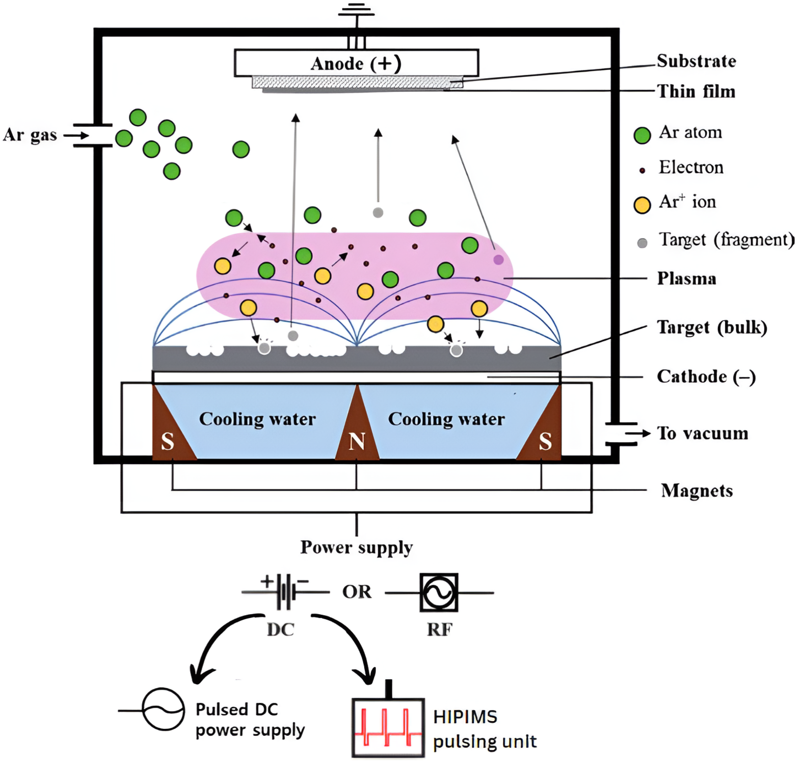
Magnetron sputtering is a technique used to deposit thin films by utilizing a gaseous plasma. Plasma, commonly known as the fourth state of matter, differs fundamentally from solids, liquids, and gases. It consists of an ionized gas, often referred to as cold plasma in the context of magnetron sputtering, as the ions and electrons are not in thermal equilibrium and the gas temperature is relatively low compared to thermal plasmas [49]. The presence of these charged particles allows plasma to conduct electricity and respond to magnetic fields, making it essential for processes like magnetron sputtering. The main difference between magnetron sputtering and other sputtering techniques is the use of magnets and magnetic fields, introduced by Penning in 1936 [50], to trap electrons in the plasma near the cathode and extend their lifetime. This increases the probability of collisions between these electrons and argon (Ar) gas atoms, ionizing them into Ar+. The magnetic field thus helps maintain a high-density plasma necessary for efficient sputtering.
A simple schematic is shown in Figure 3, representing the main components of a magnetron sputtering system, and illustrating the dynamics of ions and electrons. The diagram highlights the vacuum chamber, with a target material (cathode) and an anode, it depicts the spiral movement of electrons and the direct paths of the ions towards the cathode.
In a standard magnetron sputtering process, the chamber is initially evacuated to achieve a high vacuum, which helps to significantly reduce the partial pressures of any residual gases and contaminants [52]. After achieving the base pressure, argon gas is introduced into the chamber, and the total pressure is regulated. Plasma generation is initiated with the application of a high voltage between the cathode, which is usually positioned directly behind the sputtering target, and the anode, which is often connected to the chamber as the electrical ground. The presence of plasma ensures that there are enough high-energy ions to bombard the target material, as collisions of electrons with nearby argon atoms knock off electrons from these argon atoms, ionizing them into positive argon ions (Ar+). These Ar+ ions are then directed towards the negatively charged cathode, which leads to high-energy collisions with the target surface. Each collision has the potential to eject atoms from the target’s surface, propelling them into the vacuum environment. Knocked-off atoms traverse the vacuum and settle onto the substrate, creating a thin film [53].

3.1.1. Types of Magnet Configurations and Arrangements

Magnetron sputtering systems utilize various magnet configurations to optimize the deposition process for different applications. The primary configurations include:
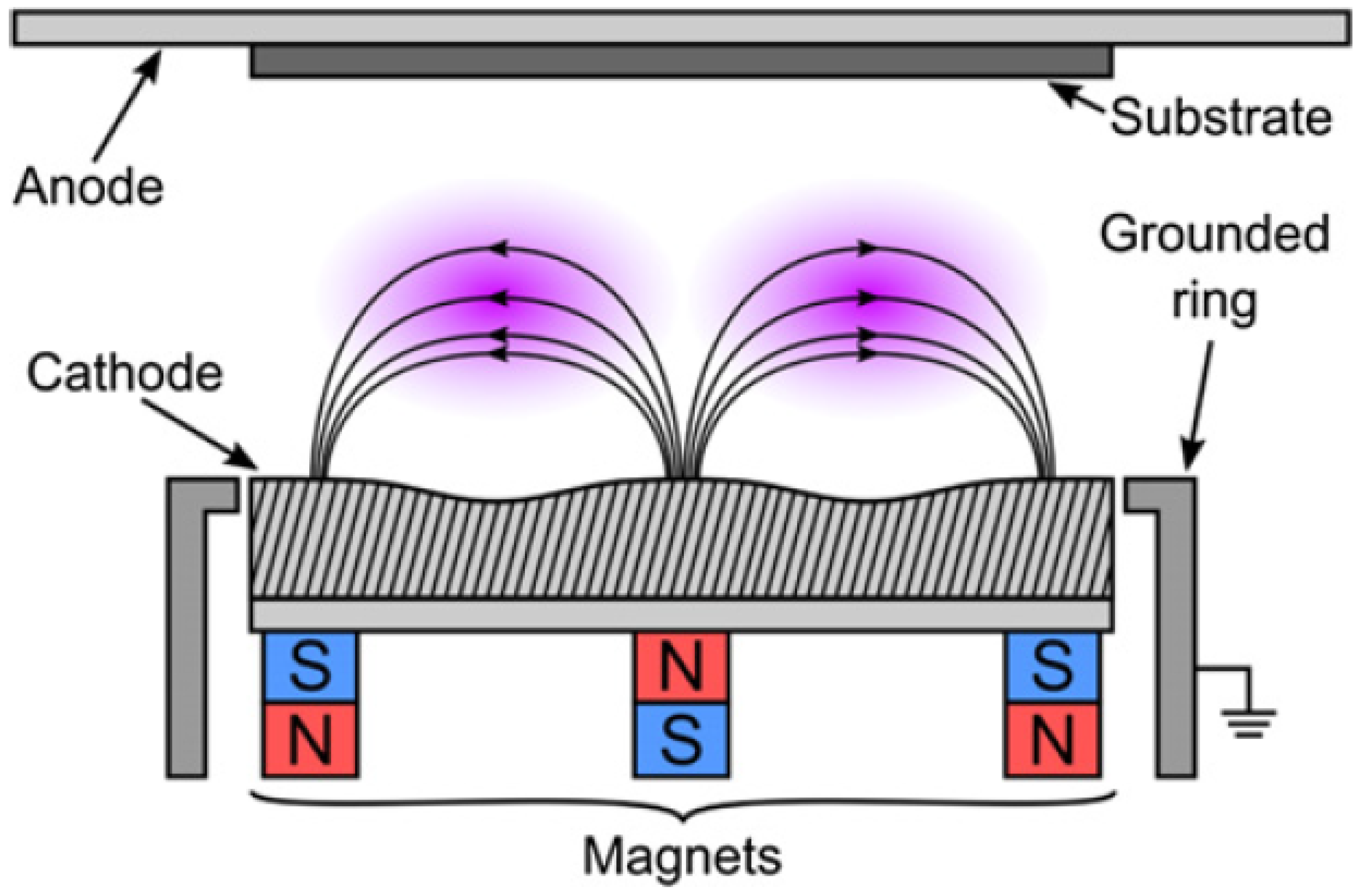
  • Planar Magnetron Sputtering: In this configuration, magnets are arranged behind a flat target. The magnetic field lines run parallel to the target surface, creating a closed loop that traps electrons near the target. This is the most common configuration and is widely used for a variety of applications [50,54], depicted in Figure 4.
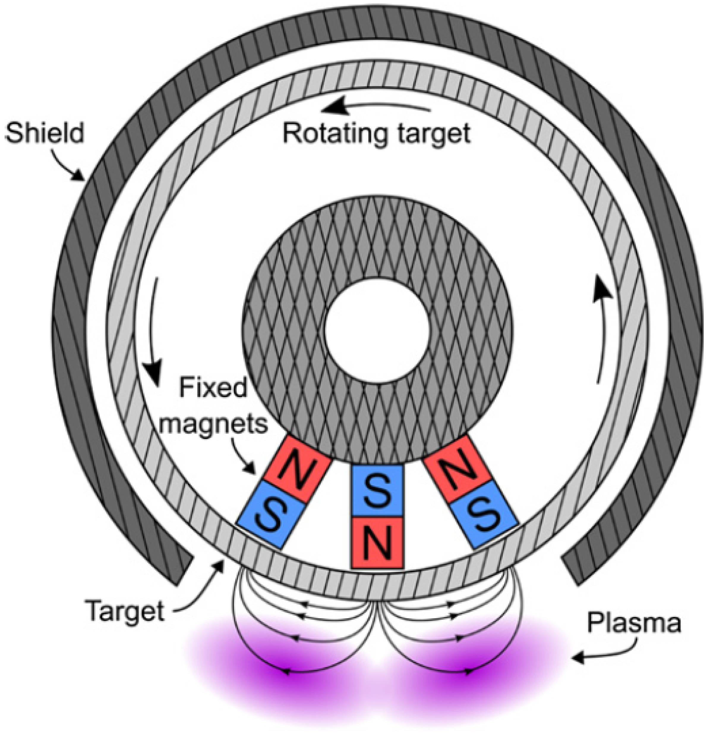
  • Rotatable Cylindrical Magnetron: In this advanced configuration, the target is a cylindrical tube that rotates around a stationary magnet assembly, as shown in Figure 5. This setup maximizes target utilization and is used for large-area coatings, such as architectural glass and display panels [50,54].
  • Balanced and Unbalanced Magnetrons: Balanced magnetrons have equal magnetic flux from the central and outer magnets, which is the case in Figure 4, in a planner configuration. On the other hand, unbalanced magnetrons have stronger outer magnets, allowing magnetic field lines to extend towards the substrate [50,54].

3.1.2. Magnetron Sputtering Categorization

Magnetron sputtering can be categorized based on its power delivery system. In DC magnetron sputtering, a continuous direct current (DC) induces a stream of electrons from the cathode to the anode. This electron flow causes the argon gas to ionize, creating a plasma state, and the target material is sputtered onto the substrate. Pulsed DC magnetron sputtering (PDC MS) employs periodic interruptions in the DC power supply to reduce ion bombardment damage. High-Power Impulse Magnetron Sputtering (HIPIMS) uses short pulses of high power to generate a denser plasma compared to conventional DC sputtering, enhancing film quality and minimizing target damage. For Radio Frequency (RF) magnetron sputtering, an alternating current (AC) at radio frequencies is used to generate a plasma state, allowing for more uniform ionization and deposition of dielectric target materials and the alternate polarity curbs the charge buildup which could cease the discharge of atoms [50].

3.2. Pre-Experimental Steps for AlN Deposition in Magnetron Sputtering Methods

For optimal AlN deposition, certain pre-experimental steps should be carefully carried out, including the preparation and cleaning of the substrate and the aluminium target (either pure or doped), adjusting the sputtering setup, chamber deposition parameters, N2/Ar ratio, processing pressure, and balancing the magnetron power. The characterization techniques used post deposition are crucial for determining the crystallographic structure, topology, sectional architecture, and piezoelectric characteristics of the AlN films.

3.2.1. Substrate Cleaning

Normally, the cleaning process includes soaking the substrate or wafer in acetone, and subjecting it to an ultrasonic cleaning process for a duration of ten minutes. This is followed by a thorough rinse with isopropanol and a subsequent drying using nitrogen gas. Such surface preparation is aimed at removing contaminants that could compromise the integrity of the deposited AlN films [41]. Depending on the type of substrate in use, slight variations in the cleaning procedure may be employed; for example, C. K. Lee et al. used an ultrasonic bath with isopropyl alcohol for 15 min to remove surface impurities on a glass substrate before depositing the AlN using RF magnetron sputtering [55]. Another cleaning method used by D.L. Maa et al. involved a glow discharge with argon ions to remove surface contaminants on a silicon (Si) wafer before depositing AlN through high-power impulse DC magnetron sputtering [56]. These cleaning methodologies have been shown to improve film adhesion.

3.2.2. Target Preparation and Positioning

The purity of the aluminum (Al) target used in magnetron sputtering is often maintained at a high level, typically around 99.999%, to ensure optimal results [41,55,56]. Prior to the sputtering process, the target is cleaned to remove any surface oxides or contaminants. Sputtering can be used for cleaning the target surface; as for Maa et al., the Al target was cleaned using a 2A DC sputtering for 5 min [56,57]. The distance between the target and the substrate is a critical parameter in DC magnetron sputtering, as it directly influences the kinetic energy and spatial distribution of the sputtered atoms during deposition. Variations in this distance can significantly affect the quality and properties of the deposited films, by affecting their crystal size, lattice constants, and chemical composition [58]. An optimal distance is essential to achieve uniform plasma density and energy distribution, as experienced by Dong-Woo Ko et al. [59]. Typically, in DC magnetron sputtering, the target-to-substrate distance can range from a few centimeters to over a dozen centimeters [41]. In contrast, high-power impulse DC magnetron sputtering (HiPIMS) often employs a shorter target-to-substrate distance, such as the 60 mm specified by Maa et al. [56], which increases the kinetic energy of the sputtered particles due to the reduced mean free path in the chamber. This shorter distance leads to a more focused and directed flux of ions and neutral species, which improves the film’s morphology [60].

3.3. Sputtering Conditions and Deposition Parameters for Magnetron Sputtering of AlN Films

Prior to deposition, vacuuming the sputtering environment is crucial for minimizing contamination and ensuring the growth of high-quality films. The specific technology employed in magnetron sputtering significantly influences the process parameters. This section examines the various categories of magnetron sputtering, including RF magnetron sputtering, DC magnetron sputtering, and high-power impulse magnetron sputtering (HiPIMS).

3.3.1. RF Magnetron Sputtering Conditions and Related Work

Lee et al. [55] investigated the RF magnetron sputtering process to deposit AlN films on glass substrates at room temperature. They used a Cryo Vacuum Chamber (CVC) RF magnetron sputtering machine with a high-purity aluminum target, maintaining a target-to-substrate distance of 24 cm. The substrates were ultrasonically cleaned, and the chamber pressure was reduced to approximately 10 6 Torr. To explore the effects of different deposition conditions, they varied RF power from 300 W to 800 W at a fixed sputtering pressure of about 5 mTorr in a pure nitrogen (N2) atmosphere. They also adjusted the sputtering pressure from 3.69 to 9.65 mTorr while keeping RF power constant at 800 W and modified argon (Ar) gas flow rates from 1 to 5 sccm, adjusting N2 flow to maintain a total flow rate of 10 sccm, with RF power and pressure held constant at 800 W and approximately 5 mTorr, respectively.
X-ray diffraction (XRD) results from [55] indicated that higher RF power promotes the (002) orientation and increases the deposition rate. Varying the sputtering pressure affected the film’s structural orientation but not the deposition rate significantly. Introducing argon gas enhanced the deposition rate but caused a shift in orientation from (002) to (101) as the argon ratio increased. The optimal conditions for achieving a highly (002)-oriented AlN film were identified as 800 W RF power and around 6 mTorr sputtering pressure in a pure N2 atmosphere.
Another investigation by Wei et al. [61] into aluminum nitride (AlN) film fabrication using RF magnetron sputtering focused on understanding distinct orientation preferences on silicon (Si) wafers. The study revealed a shift in preferred orientation from (002) to (100) with increasing distance between target and substrate, as depicted in Figure 6. Cross-sectional SEM images illustrated that the crystalline orientation strongly influenced the film’s morphology. The (002)-oriented AlN films exhibited dense columnar grains, while (100)-oriented films lacked a columnar structure. Additionally, mixed orientation growth resulted in a unique rose-like microstructure. The thickness of the AlN films varied with orientation, decreasing from (002) to (100) orientation due to surface energy minimization.
The SEM images in Figure 6 provide crucial insights into the relationship between crystalline orientation and film morphology in aluminum nitride (AlN) thin films deposited via RF magnetron sputtering. Each image visually represents a distinct orientation preference: (002), (100), and mixed orientations. Figure 6a highlights AlN films with a (002) orientation, characterized by dense columnar grains essential for high crystallinity and piezoelectric response. Conversely, Figure 6b showcases films with (100) orientation, lacking columnar grain structure, making them ideal for surface passivation in electronics. Furthermore, Figure 6c presents mixed orientation films, offering tailored properties advantageous for enhancing mechanical stability in thin-film devices. Accompanied by Figure 6d–f, which illustrate the morphology evolution with orientation, these images provide a comprehensive understanding of how different orientations influence film growth. This insight aids in optimizing the deposition processes to achieve the desired film properties, thereby contributing significantly to the advancement of AlN thin-film technology.
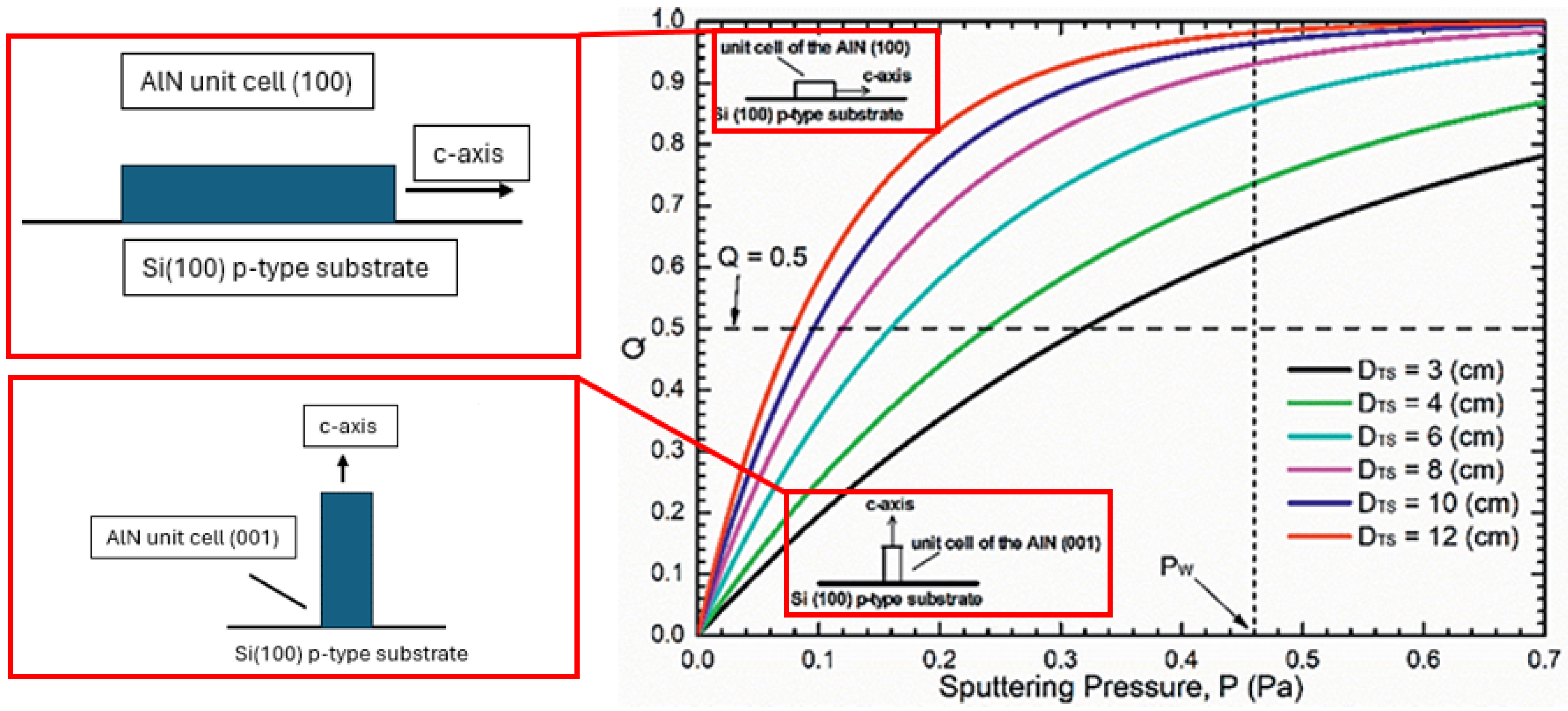
A novel method was devised for growing highly (100)-oriented aluminium nitride (AlN) thin films on (100) Si substrates under poor vacuum conditions using radio frequency (RF) magnetron sputtering [1]. This method enabled the prediction of optimal deposition conditions, resulting in high-quality films with desirable stoichiometry (Al/N ratio ≈ 1:1) and low oxygen concentration (<10). Throughout the deposition process, the substrate was maintained at floating potential, while parameters such as temperature, nitrogen flow, RF power, and sputtering pressure were held constant. Variations in the target–substrate distance and deposition time were systematically explored, as shown in Figure 7. The results from [1] revealed that films grown outside the cathodic sheath region exhibited good crystallinity and preferred (100) orientation, and under specific working pressure and mean free path conditions, films can grow with the preferred orientation of the c-axis, a direction of [001], parallel to the substrate surface. Within the cathodic sheath region, conditions are less favorable for the formation of high-quality films due to increased ion bombardment and potential thermal effects that can disrupt the growth process. Beyond the cathodic sheath, the mean free path of gas species is significantly smaller than the distance between the target and the substrate, which results in frequent collisions among aluminium and nitrogen molecules. These collisions facilitate the formation of dimers (Al-N), which contribute to a more uniform deposition on the substrate which enhances the crystal structure. The energy of the arriving species is controlled by adjusting the substrate temperature, working pressure, and the target–substrate distance. High energy levels favor the growth of AlN films with the c-axis ([001] direction) parallel to the substrate, while lower energy levels promote the preferred (100) orientation. The choice of our deposition technique allows for precise control over the growth environment, and the minimization of impurities like oxygen, which may adversely affect film quality. Hence, these factors create optimal conditions for achieving AlN films with high crystallinity and desired orientations. These findings underscore the potential of RF magnetron sputtering for fabricating highly (100)-oriented AlN films suitable for surface acoustic wave (SAW) sensing devices.
Moving forward, adjusting critical parameters such as the mean free path L, temperature T, pressure P, and target–substrate distance allows for control over the crystal orientation in the (100) and (001) directions during AlN growth, as these parameters determine the energy imparted by plasma species onto the substrate. This regulation directly affects both the mean free path L and the collision probability Q of these species within the deposition environment, as illustrated in Figure 7. The mean free path L (measured in meters) represents the average distance a particle travels before colliding with another particle during the deposition process. It is influenced by temperature T, pressure P, and the size of the plasma particles, as described in Equation (1). The theoretical framework linking these parameters is encapsulated in the mean free path equation, where the Boltzmann constant k B = 1.38 × 10 23 J / K relates the kinetic energy of particles to temperature, expressing energy on a per-particle basis in Joules per Kelvin. Furthermore, the mean free path L is related to the collision probability Q, which is given in Equation (2) and is calculated after the species pass through a target–substrate distance D TS . The parameter d, defined as the ratio between the target–substrate distance and the target diameter ϕ T , influences the dependency of the ratio D TS L . For instance, if the substrate is close to the target ( d < 0.5 ) , the film tends to exhibit amorphous characteristics, independent of the ratio D TS L . However, when the substrate is further away ( d > 0.5 ) , AlN peaks such as (100) and (001) become more prominent as the ratio D TS L increases. This correlation between film orientation and surface morphology highlights the significance of deposition conditions in shaping film properties [38].
L = k B T 2 · ( 4 π r mean 2 ) P
Q = 1 exp D T s L

3.3.2. Reactive Magnetron Sputtering Conditions and Related Work

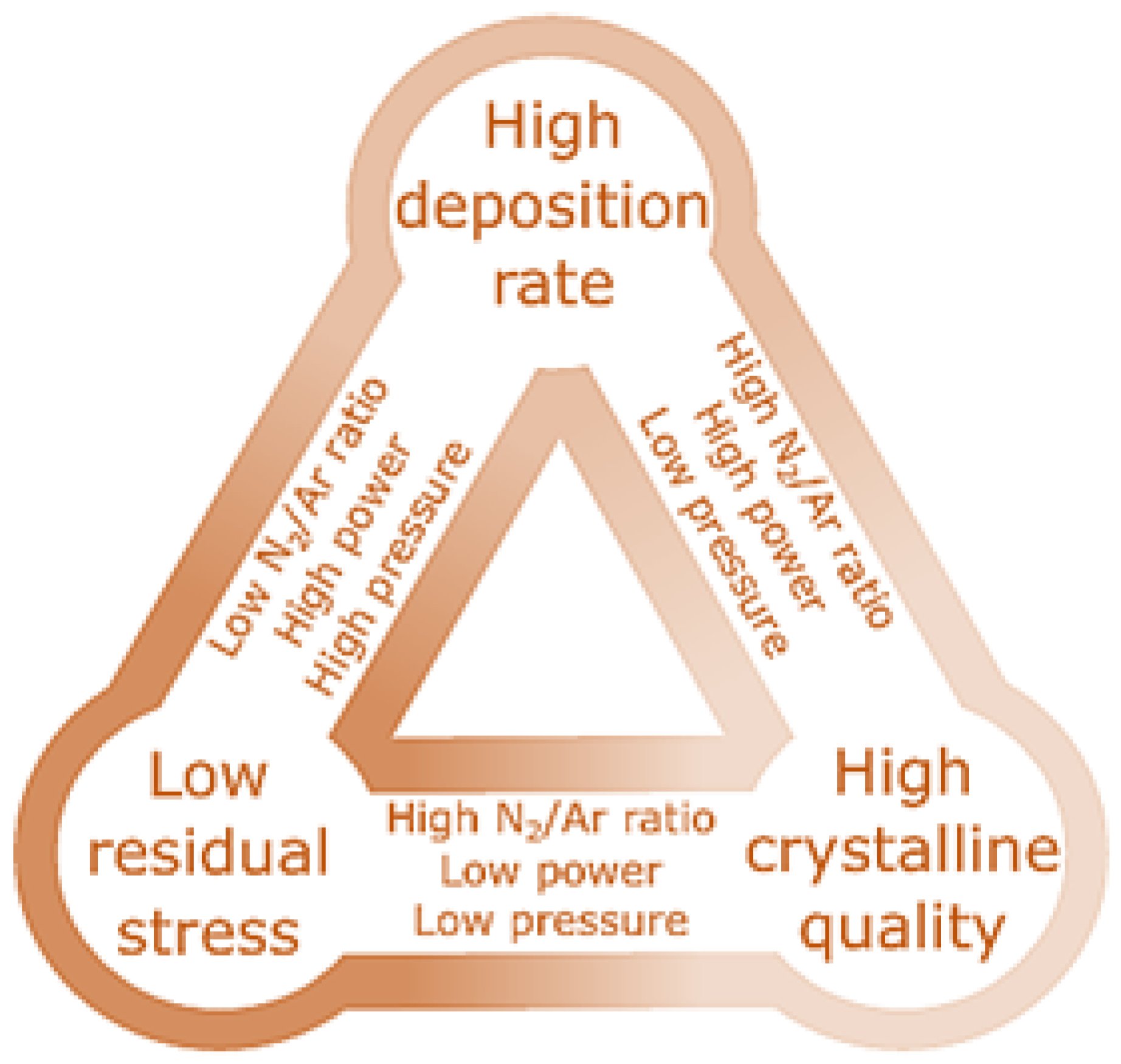
Reactive magnetron sputtering is a variation of magnetron sputtering where a reactive gas, such as nitrogen or oxygen, is introduced into the vacuum chamber along with the inert gas (typically argon). When the sputtered atoms from the target combine with the reactive gas, they form a compound film on the substrate. In the deposition of AlN thin films via reactive magnetron sputtering, achieving optimal quality involves balancing various parameters such as crystalline quality, surface roughness, residual stress, and deposition rate, alongside factors like target-to-substrate distance, pressure, and temperature, as well as gas ratios. For instance, to enhance crystalline quality and minimize surface roughness, a compromise between high N 2 / Ar gas flow ratios and low processing pressures is proposed by Sandager et al. [41], albeit with potential issues like target poisoning and reduced deposition rates, which can pose challenges for industrial applications. Reactive magnetron sputtering exacerbates this with target poisoning, where non-sputterable compounds accumulate on the target surface due to reactions with the reactive gas, diminishing sputtering efficiency and thin-film quality. Adjusting magnetron power can help balance residual stress and deposition rate, while employing lower N 2 / Ar ratios can yield acceptable quality films with higher deposition rates, illustrating the trade-offs in optimization efforts. Various studies [24,62,63] underscore these complexities. Figure 8 visually summarizes these compromises, offering guidance for achieving functional AlN films across different operational priorities.

3.3.3. DC Magnetron Sputtering Conditions and Related Work

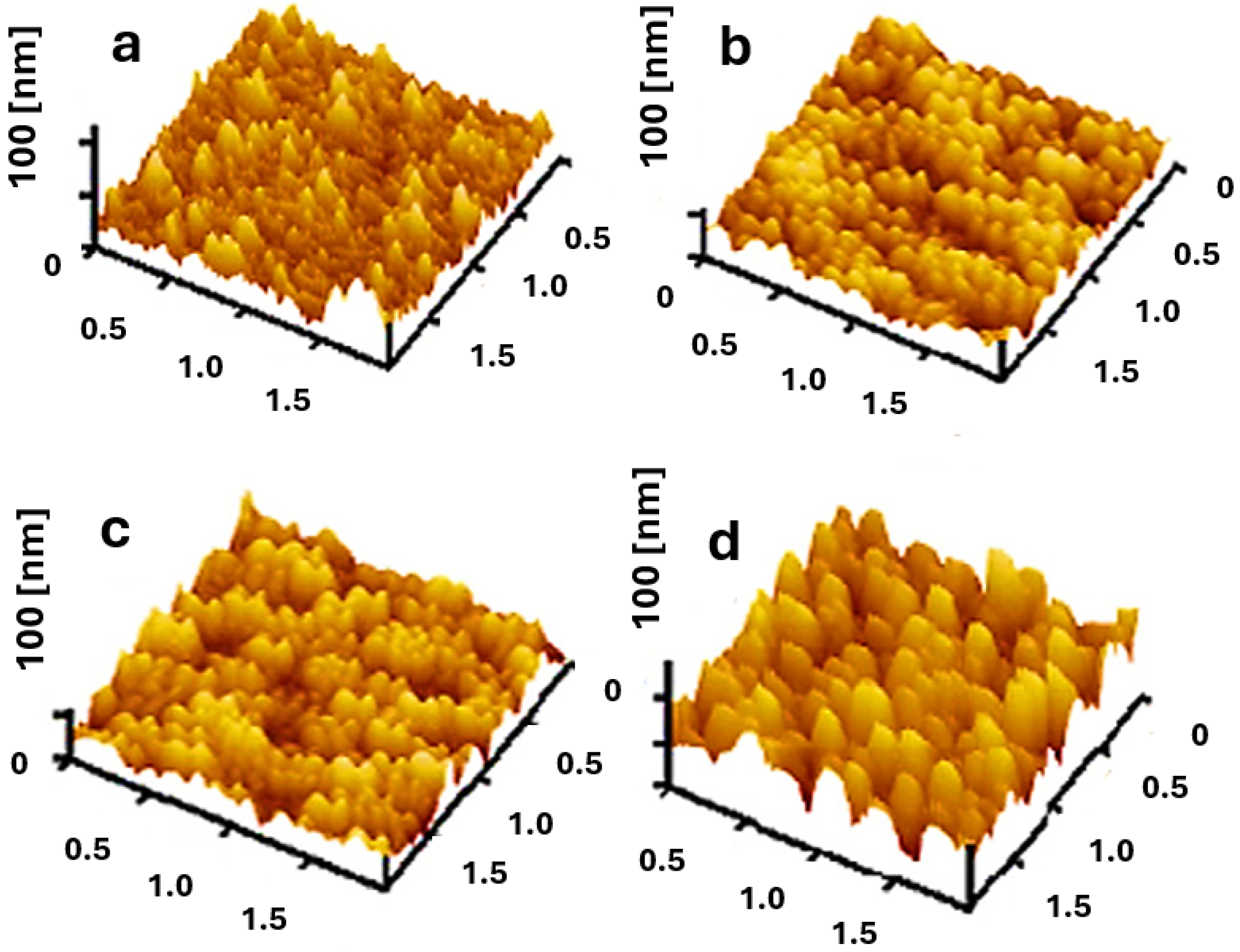
The research in the domain of DC magnetron sputtering explores the development and use of aluminum nitride (AlN) thin films to enhance heat dissipation in flexible electronics [64]. The study employs DC magnetron reactive sputtering at ambient temperature to deposit AlN films, analyzing the impact of varying deposition power on the films’ characteristics. The results revealed that increasing the deposition power boosts the deposition rate, peaking at 3.3 μm/h at 600 W. X-ray diffraction (XRD) results in [64] showed that thicker films had better crystalline quality, transitioning from disordered to ordered AlN (002) orientation. Thermal conductivity was found to be dependent on film thickness, with measured values of 7.5, 9.8, and 13.3 W/(m·K) for thicknesses of 1, 5, and 10 μm, respectively. The optimal power for achieving high-quality, thermally efficient AlN films was determined to be 600 W. This pivotal finding guided the subsequent investigation into the surface morphology of the deposited films. Illustrated in Figure 9a–d, the atomic force microscopy images offer a comprehensive analysis of the surface characteristics across different power levels. At 300 W (Figure 9a), the films had smaller grains and smoother surfaces, with a mean surface roughness (Ra) of 7.2 nm and a grain diameter (D) of 40.1 nm. When the power was increased to 400 W (Figure 9b), the grain size grew to 138.4 nm and surface roughness increased to Ra 14.2 nm. Further increasing the power to 500 W (Figure 9c) led to a grain diameter of 186.6 nm and a similar surface roughness of around 14.0 nm. At the maximum power of 600 W (Figure 9d), the films exhibited the largest grain size of 250.8 nm and a surface roughness of Ra 14.6 nm. These findings indicate that higher sputtering power results in larger grain sizes and slightly increased surface roughness, suggesting improved crystalline quality and enhanced thermal properties.
In their study, Wu et al. (2024) [65] discuss the growth parameters for aluminum nitride (AlN) thin films. To produce high-quality AlN piezoelectric thin films characterized by a highly c-axis orientation and low stress, 1 μm-thick AlN films were deposited via DC magnetron sputtering on an 8-inch Mo/AlN-interlayer/Si substrate under varied growth conditions. Optimization efforts resulted in achieving a low full width at half the maximum (FWHM) of the AlN (002) rocking curve, reaching as low as 0.905, as shown in Figure 10. The study systematically analyzed the relationship among film quality, morphology, stress, and the underlying growth mechanism of AlN films. Different morphologies and residual stresses were observed in the AlN films, attributed to variations in deposited conditions affecting sputtering particles and film grains. Additionally, the pseudo-Voigt function was employed theoretically to assess grain size and stress in the AlN film, suggesting its feasibility for evaluation when a uniform grain distribution is maintained.

3.3.4. High-Impluse DC Magnetron Sputtering Conditions and Related Work

For the high-power impulse magnetron sputtering (HiPIMS) AlN thin-film experiment by Maa D. L et al., the chamber pressure was kept below 8 × 10 4 Pa. The nitrogen (N2) gas flow rates ranged from 0 to 15 sccm, with argon (Ar) flow kept constant at 40 sccm. The pulsed power supply was set to −800 V, with a frequency of 200 Hz and pulse widths ranging from 50 to 80 μs. Substrates were cleaned using a glow discharge with Ar+ ions. As N2 flow increased, the sputtering mode transitioned from metallic (pure aluminum target surface) to transitional (partial nitridation of the target surface) and then to compound mode (complete nitridation of the target surface), resulting in an increased ion-to-neutral ratio of Al species and reduced Al flux. Higher pulse widths (80 μs) led to increased deposition rates compared to shorter ones (50 μs). Films exhibited compressive stress, which increased with N2 flow, while longer pulse widths resulted in lower residual stresses. Stoichiometric AlN films were achieved at 5 sccm for 50 μs and 8 sccm for 80 μs, confirmed by XPS analysis. They demonstrated that films deposited at 80 μs and higher N2 flows exhibited a strong (002) texture, as confirmed by XRD analysis. However, excessive ion bombardment shifted the preferred orientation to (100). At lower sputtering pressures, the mean free path of the particles is longer, resulting in higher kinetic energy for the Al and N atoms. This higher energy allows the atoms to migrate more effectively, favoring the growth of the (002) orientation due to its lower surface energy and higher stability. As the sputtering pressure increases, the mean free path decreases, leading to more collisions and reduced kinetic energy of the particles. This reduction in energy makes it more difficult for the atoms to migrate to the (002) sites, causing a shift to the (100) orientation, which requires less energy to form under these conditions.
Additionally, the films showed increased surface roughness in compound mode and a dense, compact morphology. There can be several impacts of this increased surface roughness on the optical, electrical, and mechanical properties of the film. Optically, surface roughness can scatter light, reducing the transparency of the film. This scattering can also affect the refractive index and the optical band gap of the film. For example, a rougher surface can lead to a lower refractive index compared to bulk AlN due to the presence of surface oxides and non-stoichiometric phases. Increased roughness can also introduce defects and grain boundaries, which can act as scattering centres for charge carriers. This can degrade the electrical properties of the film, such as its conductivity and dielectric strength. Rough surfaces can also lead to stress concentration points, which can affect the mechanical integrity of the film. This can be particularly important in applications where the film is subjected to mechanical stress or thermal cycling. Despite the increased surface roughness, AlN films can still exhibit a dense and compact shape. This is because the columnar growth mode, typical in sputtered films, can lead to densely packed columns that are closely aligned. The cross-sectional morphology of the films often shows highly parallel columnar crystals, which contribute to the overall dense structure of the film [56].
Another investigation of AlN thin-film deposition by Jyotish Patidar et al. utilized synchronized HiPIMS, where the substrate bias was timed to coincide with the arrival of Al-rich species during each HiPIMS pulse. The research also included a comparison with the thin films deposited using direct-current magnetron sputtering (DCMS) under similar conditions, and the experimental results were compared to those of HiPIMS. The substrates, p-type silicon wafers (001), were cleaned ultrasonically and maintained at a temperature of 280 °C during deposition. A 2-inch aluminum (Al) target with 99.999% purity was used, positioned 12 cm from the substrate, and angled at 26° relative to the normal substrate. The base pressure was maintained at less than 1 × 10 6 Pa to ensure minimal contamination. The working pressure was set at 0.3 Pa with a gas mixture of argon (Ar) and nitrogen (N2) flowing at 20 sccm and 10 sccm, respectively. For HiPIMS, the pulse width was 10 μs, and the frequency was 7.5 kHz. A pulsed substrate bias of −30 V was applied, synchronized with the HiPIMS pulse, with a duration of 40 μs and a delay of 15 μs relative to the onset of the HiPIMS pulse. Between pulses, the substrate potential was actively controlled and set to 0. The ion energy distribution functions (IEDFs) for Al, N, and Ar were measured using an EQP-300 Hiden analytical mass spectrometer positioned at the substrate’s working distance. Time-resolved measurements were synchronized with the HiPIMS pulse to capture the ion arrival times and their energies. AlN films deposited using HiPIMS were compared to those deposited with DCMS under similar conditions to assess differences in ion flux, kinetic energy, and film growth dynamics.
The HiPIMS process involved applying highly energetic pulses to the sputtering target, resulting in higher ionization rates and increased adatom mobility. This approach significantly improved the texture and crystalline quality of the AlN films, achieving a pronounced c-axis orientation with uniform grain polarization while also reducing defect-related stresses. The process resulted in a denser, more compact columnar structure, crucial for piezoelectric applications such as surface acoustic wave (SAW) devices [66].
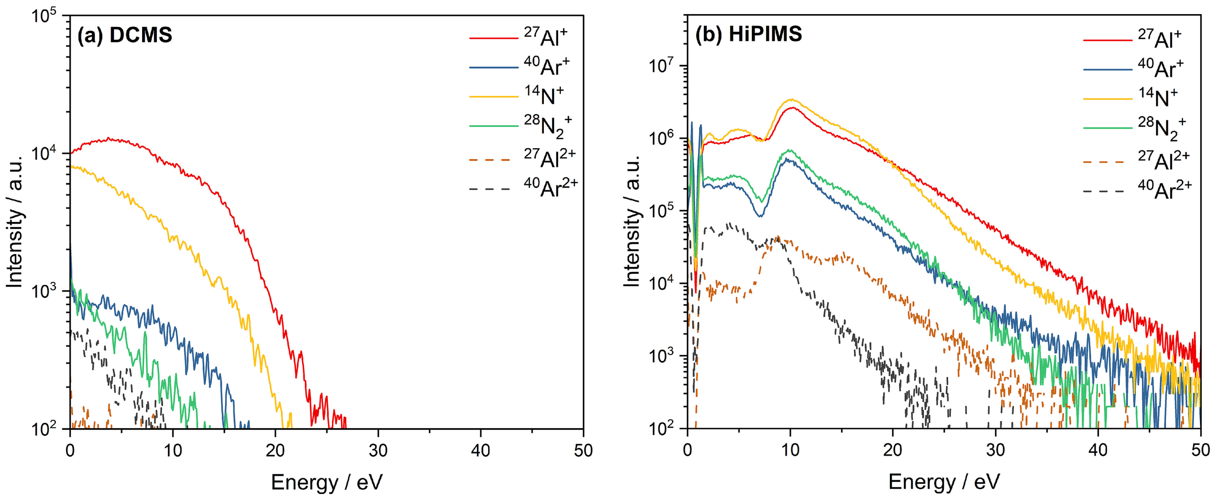
Figure 11 compares the ion energy distribution functions (IEDFs) for both DCMS and HiPIMS. The graphs illustrate the intensity of various ion species (such as Al + , Ar + , N + , N 2 + , and Ar + 2 ) as a function of their energy. The key observation is that HiPIMS generates a significantly higher ion flux and higher kinetic energies compared to DCMS. Specifically, the median kinetic energy of Al + ions increases from about 6.6 eV in DCMS to 10.7 eV in HiPIMS. This higher ion energy in HiPIMS is attributed to the high-power pulses used, which result in a more energetic plasma and a higher degree of ionization. Consequently, HiPIMS produced denser and more crystalline films due to the enhanced ion bombardment during deposition [66].

3.4. Comparative Study of Synthesis of AlN with Various Deposition Techniques

Various deposition techniques have been employed to synthesize AlN thin films, each with its advantages and challenges. Here, we provide an overview and comparison of different methods used for forming AlN thin films.

3.4.1. Dual Ion Beam Sputtering

Two ion beams are used in dual ion beam sputtering: one for sputtering the target material and another to help the film grow on the substrate. Improved control over the composition and quality of the film is possible with this technology. In comparison to single ion beam systems, this results in better control over film composition as well as increased film adhesion and density, but it also necessitates more sophisticated and costly equipment [67].

3.4.2. Molecular Beam Epitaxy (MBE)

In the highly regulated technique of molecular or atomic beam epitaxy (MBE), the substrate is exposed to beams of various species in an ultra-high vacuum setting. This process is well known for yielding single-crystal films of excellent purity with exact control over composition and thickness. It produces an epitaxial film of superior quality and allows for exact control over film growth. Low deposition rates, expensive equipment, and ongoing maintenance must all be tolerated as a trade-off [68].

3.4.3. Chemical Vapor Deposition (CVD)

In order to create the desired layer, CVD uses chemical interactions between gaseous precursors and a heated substrate surface. Variants of plasma-enhanced CVD (PECVD) can reduce the necessary substrate temperatures. It has the ability to uniformly and evenly deposit high-quality films across vast regions. Additionally, because of the high temperature and intricate process control, there is a chance of contamination linked to precursors [69].

3.4.4. Pulsed Laser Deposition (PLD)

PLD deposits the film onto the substrate by ablating a target material with high-energy laser pulses, which produce a plasma plume. Complex compounds with stoichiometric transfer from target to substrate can be deposited using this approach. It is able to deposit different elements, such as AlN, and has a high stoichiometric transfer [70].
Each technique offers unique advantages and poses specific challenges. The choice of deposition method depends on the desired film properties, application requirements, and available resources. Below is a summary Table 2 comparing key parameters for these techniques.

3.5. Doping and Coating Al Target with Other Materials

The doping of aluminium target (Al) with other dopant materials during deposition with magnetron sputtering techniques is carried out by combining Al with the other material before sputtering and using the compound as a target instead of the Al target. The introduction of materials like scandium (Sc), erbium (Er) and chromium (Cr) into AlN films has been a focal point of research, due to the resulting films with improved piezoelectric response, surface roughness, high resistance to stress and thermal stability of frequency.

3.5.1. Scandium Doping

Mei Wang et al. investigated the introduction of Sc into the AlN, with 6% Sc and the use of DC Magnetron Sputtering. The target-to-substrate distance maintained during the sputtering process was 8 cm. This doping led to a reduction in surface roughness from 2.1 nm to 1.18 nm and a decrease in film nonuniformity from 1% to 0.4% [71]. Figure 12 illustrates the surface scanning electron microscopy (SEM) image of the undoped aluminium nitride (AlN) film, and the aluminium scandium nitride (AlScN) film, which has been doped with 6% scandium. It provides a clear view of the grain distribution of the film’s surface, before and after scandium doping, showing that the Sc doping does not affect the uniformity of grain distribution and the compactness of the surface, while it can reduce the surface roughness, resulting in a smoother film surface [71]. This smoothness enhances piezoelectric performance by minimizing scattering and defects [18]. More importantly, the changes in the crystal structure caused by the incorporation of scandium increase the internal polarization of the material and significantly increase the piezoelectric coefficient (d33), which leads to a more pronounced piezoelectric response, making Sc-doped AlN films more suitable for high-performance applications such as Film Bulk Acoustic Resonator (FBAR) devices [71].

3.5.2. Chromium Doping

Chromium (Cr) doping is another approach used to modify the properties of AlN films, particularly to improve their piezoelectric activity and adjust the temperature coefficient of frequency. This method involves co-sputtering aluminum and chromium targets. V. Felmetsger and M. K. Mikhov carried out the deposition with Cr to produce AlCrN thin films, using RF magnetron sputtering and a dual-target S-gun magnetron system, with setup parameters of 40 kHz AC power applied between the two targets (95.28% aluminum and 4.72% chromium) leading to a plasma discharge. These films of AlCrN were assessed for their piezoelectric activity using solidly mounted resonator bulk acoustic wave (SMR BAW) devices and contour mode resonator (CMR) devices, in which they demonstrated lower values of Q factor and an electromechanical coupling coefficient, with values approximately at 250 and 0.55%, respectively, while the temperature coefficient of frequency (TCF) was higher (at about −68 ppm/K) compared with pure AlN films. Moreover, the surface morphology of the AlCrN film was notably different across various substrates, showing distinct variations on silicon and platinum substrates [72].

3.5.3. Chromium Coating

Another way of adding chromium to the AlN film is through a coating mechanism, which involves depositing a layer of chromium onto the AlN film surface. In a study carried out by Y.L. Su et al., the films of Cr-Al-N were prepared by unbalanced magnetron sputtering under a base pressure of 1.59 × 10 3 Pa and a working pressure of 0.37 Pa. As a result, the corrosion resistance and the electrical conductivity of the films were improved, as the Cr-Al-N coating scored a corrosion current density of 5.35 × 10 7 A / cm 2 and an electrical conductivity of 5.5 ohm.cm. This makes the coatings suitable as protective coatings for the bipolar plates of proton exchange membrane fuel cells (PEMFCs) [73].

4. Applications of AlN

The multifaceted attributes of aluminum nitride (AlN) render it highly suitable for a diverse array of applications, encompassing resonators, energy harvesting, and thermal management. Within wave resonators, such as Film Bulk Acoustic Wave Resonators (FBARs), AlN’s characteristics of low dielectric loss, high bulk acoustic wave velocity, chemical and thermal stability, moderate electromechanical coupling constant, and wide band gap, facilitate the efficient propagation of signals and resonant behavior, both of which are imperative for operational efficacy.
Aluminum nitride (AlN) exhibits several characteristics that distinguish it from other piezoelectric materials such as PZT and ZnO. One significant advantage is its high thermal stability and ability to operate effectively at elevated temperatures, making it suitable for applications in harsh environments where other materials may fail. AlN has a wide band gap of approximately 6.2 eV, which allows it to be used in high-frequency devices without significant energy loss due to dielectric heating. Unlike PZT, which is ferroelectric and can exhibit fatigue over time, AlN’s non-ferroelectric nature contributes to its durability and long-term reliability in piezoelectric applications. AlN’s lower density compared to PZT enhances its suitability for lightweight applications in micro-electromechanical systems (MEMSs) [45]. As also discussed previously, recent studies have also shown that doping AlN with elements like scandium can significantly improve its piezoelectric properties without compromising its thermal stability [74]. These unique characteristics position AlN as a superior choice for next-generation devices, requiring robust performance across various operating conditions.
In energy harvesting contexts, AlN’s favorable combination of a moderate electromechanical coupling coefficient (k) and high-quality factor (Q) position it as an optimal choice for the development of proficient piezoelectric generators, outperforming alternatives like lead zirconate titanate (PZT). There also exist examples where AlN plays a pivotal component in power electronics and high-frequency circuitry, one of the reasons being its efficacy in dissipating heat in various applications. The following section delves into the applications and utilization of AlN, particularly when produced through the magnetron sputtering technique.

4.1. Application in Wave Resonators

In the construction of resonators like the Film Bulk Acoustic Wave Resonator (FBAR), a configuration typically involves a thin piezoelectric film positioned between two electrodes, as depicted in Figure 13. When a voltage is applied across these electrodes, a resonant acoustic wave is generated within the piezoelectric layer. In this context, aluminum nitride (AlN) is the piezoelectric material for FBAR construction. AlN facilitates the conversion of electrical signals into mechanical vibrations and vice versa, thereby fostering the resonant behavior essential for the functioning of FBARs.
Aluminum nitride (AlN) facilitates efficient signal propagation due to a bulk acoustic wave velocity of approximately 11,000 m/s, the highest among alternatives like PZT and ScAlN. Its moderate electro-mechanical coupling constant indicates efficient conversion between electrical and mechanical energy. Additionally, due to its low dielectric constant, it reduces energy dissipation during signal transmission. AlN boasts excellent chemical and thermal stability, with a melting point of 2100 °C, further contributing to its suitability. Its wide band gap of 6.2 eV renders it suitable for high-frequency operations. The piezoelectric properties of AlN depend on its crystalline structure and orientation along the c-axis. Proper orientation along the c-axis enhances its piezoelectric performance [33], which can be sufficiently obtained using the sputtering process.
High-quality crystalline AlN films can be produced at lower temperatures (in the range of 500 °C) through sputtering. Parameters such as the distance between the target and substrate, pressure, N2 concentration, sputtering power, and substrate temperature influence the quality and orientation of the deposited film. Fine-tuning these parameters optimizes the performance of Film Bulk Acoustic Resonator (FBAR) devices, aiding in the optimization of deposition conditions for FBAR fabrication. The degree of crystallization, preferred orientation, and surface morphology of the deposited AlN layer serve as indicators of FBAR device effectiveness [75].

4.2. AlN-Based Energy Harvesting Application

To develop small sensors and liberate them from the bounds of battery and their limitations, alternative power sources are being developed. Among them is the concept of energy harvesting, where residual or ambient energy is utilized to harness the surrounding energy for the system. Aluminium nitride (AlN) is a material widely used in the application of energy harvesting, leveraging its conversion property from mechanical to electrical energy. While zinc oxide (ZnO), polyvinylidene fluoride (PVDF), and lead zirconate titanate (PZT) are other promising candidates, AlN stands out in certain areas.
AlN possesses a high mechanical quality factor (Q) with a moderate electromechanical coupling coefficient (k), making it a good option for designing efficient piezoelectric generators. Unlike lead zirconate titanate (PZT), AlN lacks ferroelectric properties. AlN has a low crystallization temperature, which makes its fabrication compatible with CMOS processes [76]. The piezoelectric coefficient and permittivity for AlN are approximately ≈1.55 C / m 2 and 10, respectively [77]. This results in a good energy-harvesting figure of merits not on par with that of PZT, but one that can be utilized [78]. Additionally, AlN is not harmful to humans health-wise. These unique characteristics make it suitable for applications where a non-ferroelectric piezoelectric material is required.
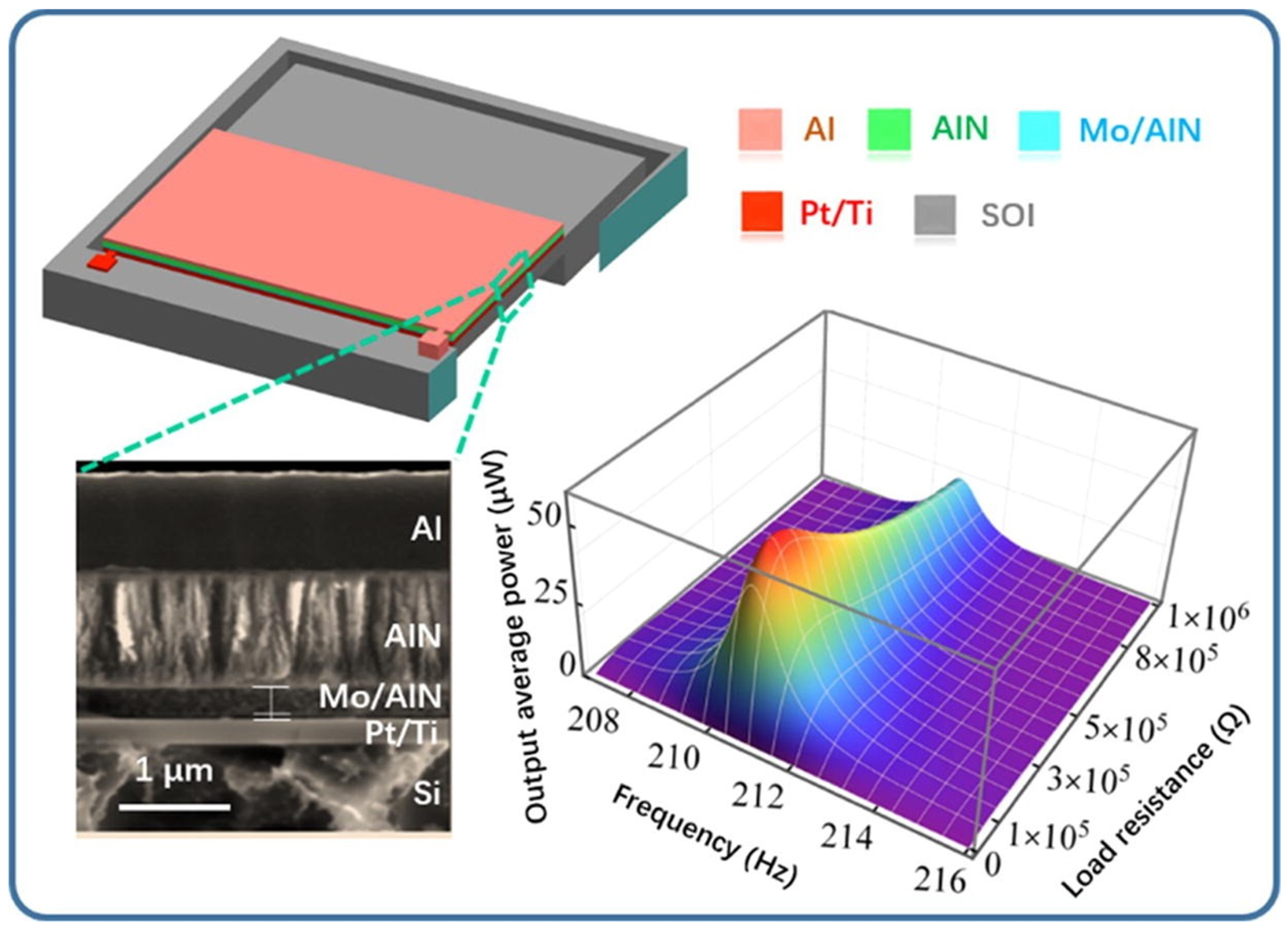
Xianming et al. [79] conducted a study on the micro-electromechanical system (MEMS) cantilever-based aluminium nitride (AlN) vibration energy harvester, as shown in Figure 14, where the c-axis-oriented AlN piezo thin film was deposited using pulsed direct-current magnetron sputtering. The prototype achieved a maximum output RMS voltage of 4.66 V at 1 g and 210.85 Hz , with an output average power of 56.4 μ W and a power density of 854.55 μ W / ( cm 3 · g 2 ) , aligning well with theoretical predictions. It provides effective guidance for design and optimization, particularly for devices with long tip mass, with potential applications in wireless sensor network nodes, such as structural health monitoring systems. A procedure of scandium doping was used by Stephan Barth et al. [24] to improve the piezoelectric properties of AlN films. These enhancements are ascribed to changes in elastic constants and an increase in piezoelectric constants. For instance, doping AlN films with scandium leads to a notable increase in the piezoelectric coefficient d 33 compared to pure AlN. It indicates that the piezoelectric coefficient d 33 increases with a higher scandium concentration in AlScN films, reaching a peak at around 40 % scandium content. This demonstrates the efficacy of these films in generating power from defined vibrations, with significant power output. Tiny AlN harvesters were introduced by Z Cao et al. [80] to harvest energy from low-frequency, two-dimensional vibrations. They used a stainless steel substrate with high fracture toughness and yield strength to enhance output power and reduce resonant frequency. AlN films were deposited on the substrate to fabricate the harvesters. This demonstrates that magnetron sputtering is a reliable and repeatable process for depositing good-quality AlN. In this way, novel harvesters using AlN are being developed to enhance the applicability of AlN. The sputtering technique offers an advantage over other techniques due to its low price point, relatively simple process with fewer precursor chemicals involved, moderate uniformity, and high scalability compared to CVD and PVD techniques.

4.3. AlN Applications in Thermal Management

Aluminium nitride (AlN) possesses a high thermal conductivity similar to metals like stainless steel, ranging from 2 to 200 W . m 1 K 1 . This notable thermal conductivity facilitates efficient heat transfer away from heat-generating components, aiding in preventing overheating, as AlN can withstand temperatures well above 1000 °C without significant degradation. The unique combination of thermal properties makes AlN suitable for various applications such as heat sinks, substrates, thermal interface materials, and packaging components, effectively dissipating heat and maintaining device performance [81,82]. For example, Elladan et al. [83] developed AlNB for effective thermal management applications in solid-state devices like LEDs at varying power levels. They achieved a lower thermal resistance of 8.5 ( K / W ) .
A technique for depositing thin films of aluminium nitride (AlN) with different thicknesses, ranging from 100 nm to 1.7 μm at low temperatures (<100 °C), was presented by C. Perez et al. [84]. By controlling deposition conditions, they achieved a wide range of thermal conductivity (36–104 W m 1 K 1 ) in 600 nm films. This highlights that there are methods to optimize AlN for specific thermal management applications in integrated circuits.
Aluminium nitride (AlN) thin films, deposited using sputtering techniques, present diverse applications. They can serve as dielectric layers, barrier coatings, or passivation layers in electronic devices, enhancing their performance and reliability, particularly in high-power and high-frequency applications [85]. Additionally, AlN thin films find utility in optoelectronics and photonics as waveguides, optical filters, or substrates for epitaxial layer growth, owing to their wide band gap and UV and visible spectrum transparency. Thus, AlN thin films offer a wide range of possibilities across thermal, optical, and mechanical domains, making them promising materials for advancing technology and magnetron sputtering a reliable deposition process to accomplish it.

5. Summary and Outlook

In conclusion, our review provides a comprehensive evaluation of magnetron sputtering for the deposition of high-quality AlN films based on the literature, with a focus on controlling orientation and optimizing film properties. By systematically examining the effects of key deposition parameters—such as working pressure, RF power, substrate temperature, and target-to-substrate distance, we have demonstrated the critical role these factors play in determining the quality and orientation of AlN films. Our results underscore that the precise control and optimization of these parameters are crucial for tailoring film properties to meet specific application requirements in electronics, optics, and sensor technologies.
The adaptability of sputtering parameters, combined with conventional temperature-dependent structural growth, enables the formation of advanced structures with improved deposition rates. This positions magnetron sputtering as a valuable technique in semiconductor manufacturing, offering opportunities to produce high-quality AlN films through various methods, including RF, DC, and impulse magnetron sputtering. Each technique provides unique advantages that can be harnessed to enhance AlN growth, making it suitable for a wide range of applications, such as wave resonators, energy harvesting, thermal management, and photonics.
Despite the significant progress made in understanding the relationship between deposition parameters and the resulting film properties, further research is necessary to explore AlN films’ behavior under extreme or elevated environmental conditions. Investigating the performance of AlN films in such challenging environments could unveil new applications and further expand their utility.
Future research should aim at further refining the deposition process to push the boundaries of AlN film quality and functionality. This includes investigating alternative seed materials to enhance nanostructure formation, optimizing deposition conditions for a variety of substrate types, and systematically studying the impact of additional parameters such as gas flow rates and substrate bias voltage. Additionally, the development and implementation of in-situ monitoring techniques during deposition can provide real-time insights into the growth mechanisms, enabling the production of more uniform and high-quality films. Such advancements could significantly enhance the reproducibility and scalability of the deposition process.

Author Contributions

Conceptualization, N.A.K.J., V.P., M.A.H.M., A.S. and K.W.; Investigation, N.A.K.J., V.P., M.A.H.M., A.S. and K.W.; Project administration, N.A.K.J. and K.W.; Supervision, K.W.; Visualization, N.A.K.J., V.P., M.A.H.M., A.S. and K.W.; Writing—original draft, N.A.K.J., V.P., M.A.H.M., A.S. and K.W. All authors contributed equally to this work. All authors have read and agreed to the published version of the manuscript.

Funding

This research received no external funding.

Conflicts of Interest

The authors declare no conflicts of interest.

References

  1. Cunha, C.L.A.; Pimenta, T.C.; Fraga, M.A. Development and Applications of Aluminum Nitride Thin Film Technology. In Thin Films; Yang, D., Ed.; IntechOpen: London, UK, 2022. [Google Scholar] [CrossRef]
  2. Yen, T.T.; Hirasawa, T.; Wright, P.K.; Pisano, A.P.; Lin, L. Corrugated aluminum nitride energy harvesters for high energy conversion effectiveness. J. Micromechanics Microengineering 2011, 21, 085037. [Google Scholar] [CrossRef]
  3. Elfrink, R.; Kamel, T.M.; Goedbloed, M.; Matova, S.; Hohlfeld, D.; van Andel, Y.; van Schaijk, R. Vibration energy harvesting with aluminum nitride-based piezoelectric devices. J. Micromechanics Microengineering 2009, 19, 094005. [Google Scholar] [CrossRef]
  4. Elfrink, R.; Renaud, M.; Kamel, T.M.; de Nooijer, C.; Jambunathan, M.; Goedbloed, M.; Hohlfeld, D.; van Andel, Y.; van Schaijk, R. Vacuum-packaged piezoelectric vibration energy harvesters: Damping contributions and autonomy for a wireless sensor system. J. Micromechanics Microengineering 2010, 20, 104001. [Google Scholar] [CrossRef]
  5. Bu, G.; Ciplys, D.; Shur, M.; Schowalter, L.J.; Schujman, S.; Gaska, R. Surface acoustic wave velocity in single-crystal AlN substrates. IEEE Trans. Ultrason. Ferroelectr. Freq. Control 2006, 53, 251–254. [Google Scholar] [CrossRef] [PubMed]
  6. Shelton, S.; Chan, M.L.; Park, H.; Horsley, D.; Boser, B.; Izyumin, I.; Przybyla, R.; Frey, T.; Judy, M.; Nunan, K.; et al. CMOS-compatible AlN piezo electric micromachined ultrasonic transducers. In Proceedings of the 2009 IEEE International Ultrasonics Symposium, Rome, Italy, 20–23 September 2009; pp. 402–405. [Google Scholar]
  7. Horsley, D. Aluminum nitride pMUT based on a flexurally-suspended membrane. In Proceedings of the 2011 Solid State Sensors, Actuators and Microsystems Conference, Beijing, China, 5–9 June 2011. [Google Scholar]
  8. Yokoyama, T.; Iwazaki, Y.; Nishihara, T.; Ueda, M. Analysis on electromechanical coupling coefficients in AlN-based bulk acoustic wave resonators based on first-principle calculations. In Proceedings of the 2012 IEEE International Ultrasonics Symposium, Dresden, Germany, 7–10 October 2012; pp. 551–554. [Google Scholar] [CrossRef]
  9. Hartnett, T.M.; Bernstein, S.D.; Maguire, E.A.; Tustison, R.W. Optical properties of ALON (aluminum oxynitride). In Proceedings of the Window and Dome Technologies and Materials V, Orlando, FL, USA, 27 June 1997. [Google Scholar]
  10. Fan, Z.; Qin, Z.; Sun, Z.; Wu, H. Broad Spectrum Detector Based on AlN Crystal. J. Phys. Conf. Ser. 2022, 2350, 012013. [Google Scholar] [CrossRef]
  11. Bickermann, M.; Epelbaum, B.M.; Filip, O.; Heimann, P.J.; Nagata, S.; Winnacker, A. UV transparent single-crystalline bulk AlN substrates. Phys. Status Solidi 2010, 7, 21–24. [Google Scholar] [CrossRef]
  12. Xu, X.; Huang, X.; Wang, X.; Kang, J.; Zheng, Y.; Chen, X. Aluminum Nitride Film and Preparation Method and Application Thereof. CN111690907A. 22 September 2020. Available online: https://www.iprdb.com/patent/CN111690907A.html#/basic (accessed on 2 September 2023).
  13. Park, J.H.; Steckl, A.J. Laser action in Eu-doped GaN thin-film cavity at room temperature. Appl. Phys. Lett. 2004, 85, 4588–4590. [Google Scholar] [CrossRef]
  14. Pearton, S.J.; Zolper, J.C.; Shul, R.J.; Ren, F. GaN: Processing, defects, and devices. J. Appl. Phys. 1999, 86, 1–78. [Google Scholar] [CrossRef]
  15. Furqan, C.M.; Ho, J.Y.L.; Kwok, H.S. GaN thin film: Growth and Characterizations by Magnetron Sputtering. Surfaces Interfaces 2021, 26, 101364. [Google Scholar] [CrossRef]
  16. Anjum, F.; Ahmad, R.; Afzal, N.; Murtaza, G. Characterization of InN films prepared using magnetron sputtering at variable power. Mater. Lett. 2018, 219, 23–28. [Google Scholar] [CrossRef]
  17. Ishibe, T.; Tomeda, A.; Watanabe, K.; Kamakura, Y.; Mori, N.; Naruse, N.; Mera, Y.; Yamashita, Y.; Nakamura, Y. Methodology of Thermoelectric Power Factor Enhancement by Controlling Nanowire Interface. ACS Appl. Mater. Interfaces 2018, 10, 37709–37716. [Google Scholar] [CrossRef] [PubMed]
  18. Polewczyk, V.; Magrin Maffei, R.; Vinai, G.; Lo Cicero, M.; Prato, S.; Capaldo, P.; Dal Zilio, S.; di Bona, A.; Paolicelli, G.; Mescola, A.; et al. ZnO Thin Films Growth Optimization for Piezoelectric Application. Sensors 2021, 21, 6114. [Google Scholar] [CrossRef] [PubMed]
  19. van Deurzen, L.; Singhal, J.; Encomendero, J.; Pieczulewski, N.; Chang, C.S.; Cho, Y.; Muller, D.A.; Xing, H.G.; Jena, D.; Brandt, O.; et al. Excitonic and deep-level emission from N- and Al-polar homoepitaxial AlN grown by molecular beam epitaxy. APL Mater. 2023, 11, 081109. [Google Scholar] [CrossRef]
  20. Popov, V.; Chirumamilla, M.; Krekeler, T.; Ritter, M.; Pedersen, K. Magnetron Sputter Grown AlN Nanostructures with Giant Piezoelectric Response toward Energy Generation. ACS Appl. Nano Mater. 2023, 6, 8849–8856. [Google Scholar] [CrossRef]
  21. Hasegawa, F.; Takahashi, T.; Kubo, K.; Nannichi, Y. Plasma CVD of amorphous AlN from metalorganic Al source and properties of the deposited films. Jpn. J. Appl. Phys. 1987, 26, 1555. [Google Scholar] [CrossRef]
  22. Hisyam, M.I.; Shuhaimi, A.; Norhaniza, R.; Mansor, M.; Williams, A.; Hussin, M.R.M. Study of AlN Epitaxial Growth on Si (111) Substrate Using Pulsed Metal–Organic Chemical Vapour Deposition. Crystals 2024, 14, 371. [Google Scholar] [CrossRef]
  23. Sanz-Hervás, A.; Vergara, L.; Olivares, J.; Iborra, E.; Morilla, Y.; García-López, J.; Clement, M.; Sangrador, J.; Respaldiza, M.A. Comparative study of c-axis AlN films sputtered on metallic surfaces. Diam. Relat. Mater. 2005, 14, 1198–1202. [Google Scholar] [CrossRef]
  24. Barth, S.; Bartzsch, H.; Glöß, D.; Frach, P.; Modes, T.; Zywitzki, O.; Suchaneck, G.; Gerlach, G. Magnetron sputtering of piezoelectric AlN and AlScN thin films and their use in energy harvesting applications. Microsyst. Technol. 2016, 22, 1613–1617. [Google Scholar] [CrossRef]
  25. Fu, Y.Q.; Luo, J.K.; Nguyen, N.T.; Walton, A.J.; Flewitt, A.J.; Zu, X.T.; McHale, G.; Matthews, A.; Iborra, E.; Rowland, D.J.; et al. Advances in piezoelectric thin films for acoustic biosensors, acoustofluidics and lab-on-chip applications. Prog. Mater. Sci. 2017, 89, 31–91. [Google Scholar] [CrossRef]
  26. Badis, R.; Camus, J.; Ayad, A.; Rammal, M.; Zernadji, R.; Rouag, N.; Abdou, M.; Hetero, D. Epitaxial Growth of AlN Deposited by DC Magnetron Sputtering on Si(111) Using a AlN Buffer Layer. Coatings 2021, 11, 1063. [Google Scholar] [CrossRef]
  27. Jiang, J.; Fu, Y.; Zhang, J.; Wei, Y.; Zhang, G.; Cui, J. Growth of c-axis oriented AlN thin films on titanium alloy substrate by middle frequency magnetron sputtering. J. Vac. Sci. Technol. 2015, 33, 041509. [Google Scholar] [CrossRef]
  28. Uchiyama, S.; Nishi, N.; Makishima, A.; Miyamoto, S.; Ohmori, A.; Araki, Y. Growth of AlN films by magnetron sputtering. J. Cryst. Growth 1998, 189, 448–451. [Google Scholar] [CrossRef]
  29. Ke, G.; Lu, P.; Jiang, L.; Zhao, W.; Li, Q.; Yu, Z.; Liu, Y. Highly c-axis oriented AlN film grown by unbalanced magnetron reactive sputtering and its electrical properties. J. Alloy. Compd. 2015, 646, 446–453. [Google Scholar] [CrossRef]
  30. Mishin, S.; Oshmyansky, Y. Magnetron Deposition of AlN and ScAlN for Massproduction for BAW Devices and MEMS. In Proceedings of the 2019 IEEE International Ultrasonics Symposium, Glasgow, UK, 6–9 October 2019. [Google Scholar] [CrossRef]
  31. Behera, L.; Pandey, N.; Gupta, M. Synthesis and characterization of AlN thin films deposited using DC and RF magnetron sputtering. J. Appl. Phys. 2020. [Google Scholar] [CrossRef]
  32. Foroughi-Abari, A.; Cadien, K.C. Growth, structure and properties of sputtered niobium oxide thin films. Thin Solid Film. 2011, 519, 3068–3073. [Google Scholar] [CrossRef]
  33. Mwema, F.M.; Akinlabi, E.T.; Oladijo, O.P. A systematic review of magnetron sputtering of AlN thin films for extreme condition sensing. Mater. Today Proc. 2020, 26, 1546–1550. [Google Scholar] [CrossRef]
  34. Iqbal, A.; Mohd-Yasin, F. Reactive Sputtering of Aluminum Nitride (002) Thin Films for Piezoelectric Applications: A Review. Sensors 2018, 18, 1797. [Google Scholar] [CrossRef]
  35. Liu, W.; He, L.; Wang, X.; Zhou, J.; Xu, W.; Smagin, N.; Toubal, M.; Yu, H.; Gu, Y.; Xu, J.; et al. 3D FEM Analysis of High-Frequency AlN-Based PMUT Arrays on Cavity SOI. Sensors 2019, 19, 4450. [Google Scholar] [CrossRef]
  36. Signore, M.A.; Velardi, L.; De Pascali, C.; Kuznetsova, I.; Blasi, L.; Biscaglia, F.; Quaranta, F.; Siciliano, P.; Francioso, L. Effect of silicon-based substrates and deposition type on sputtered AlN thin films. Appl. Surf. Sci. 2022, 599, 154017. [Google Scholar] [CrossRef]
  37. Bairagi, S.; Järrendahl, K.; Eriksson, F.; Hultman, L.; Birch, J.; Hsiao, C.L. Glancing Angle Deposition and Growth Mechanism of Inclined AlN Nanostructures Using Reactive Magnetron Sputtering. Coatings 2020, 10, 768. [Google Scholar] [CrossRef]
  38. Cunha, C.L.A.; Pimenta, T.C.; Fraga, M.A. Growth and properties of sputtered highly (100)-oriented oxygenated AlN thin films for SAW sensing applications. Microsyst. Technol. 2021, 27, 3773–3782. [Google Scholar] [CrossRef]
  39. Chirumamilla, M.; Krekeler, T.; Wang, D.; Kristensen, P.K.; Ritter, M.; Popok, V.N.; Pedersen, K. Magnetron Sputter Deposition of Nanostructured AlN Thin Films. Appl. Nano 2023, 4, 280–292. [Google Scholar] [CrossRef]
  40. Ababneh, A.; Dagamseh, A.M.K.; Albataineh, Z.; Tantawi, M.; Al-Bataineh, Q.M.; Telfah, M.; Zengerle, T.; Seidel, H. Optical and structural properties of aluminium nitride thin-films synthesized by DC-magnetron sputtering technique at different sputtering pressures. Microsyst. Technol. 2021, 27, 3149–3159. [Google Scholar] [CrossRef]
  41. Sandager, M.K.; Kjelde, C.; Popok, V. Growth of Thin AlN Films on Si Wafers by Reactive Magnetron Sputtering: Role of Processing Pressure, Magnetron Power and Nitrogen/Argon Gas Flow Ratio. Crystals 2022, 12, 1379. [Google Scholar] [CrossRef]
  42. Alyousef, H.A.; Hassan, A.M.; Zakaly, H.M.H. Reactive magnetron sputtered AlN thin films: Structural, linear and nonlinear optical characteristics. J. Mater. Sci. Mater. Electron. 2023, 34, 1088. [Google Scholar] [CrossRef]
  43. Yin, J.; Zhou, B.; Li, L.; Liu, Y.; Guo, W.; Talwar, D.N.; He, K.; Ferguson, I.T.; Wan, L.; Feng, Z.C. Optical and structural properties of AlN thin films deposited on different faces of sapphire substrates. Semicond. Sci. Technol. 2021, 36, 045012. [Google Scholar] [CrossRef]
  44. Chen, G.; Li, H.; Xie, X.; Xie, L.; Wang, E.; Liu, G.; Zhang, H.; Lu, B.; Li, C.; Pei, H. Influence of nitrogen flow ratio on properties of c-axis oriented AlN films grown by RF magnetron sputtering. Appl. Phys. A 2021, 127, 819. [Google Scholar] [CrossRef]
  45. Desideri, D.; Bernardo, E.; Corso, A.J.; Moro, F.; Pelizzo, M.G. Electrical Properties of Aluminum Nitride Thick Films Magnetron Sputtered on Aluminum Substrates. Materials 2022, 15, 2090. [Google Scholar] [CrossRef]
  46. Uesugi, K.; Shojiki, K.; Xiao, S.; Kuboya, S.; Miyake, H. Effect of the Sputtering Deposition Conditions on the Crystallinity of High-Temperature Annealed AlN Films. Coatings 2021, 11, 956. [Google Scholar] [CrossRef]
  47. Liu, S.; Li, Y.; Tao, J.; Tang, R.; Zheng, X. Structural, Surface, and Optical Properties of AlN Thin Films Grown on Different Substrates by PEALD. Crystals 2023, 13, 910. [Google Scholar] [CrossRef]
  48. Sanjeeva, S.; Rudresh, J.; Vinayakumar, K.B.; Nagaraja, K.K. A strong dependence of sputtering power on c-axis oriented aluminium nitride on Si (111): A structural and electrical study. IET Nanodielectrics 2024, 7, 7–17. [Google Scholar] [CrossRef]
  49. Wang, F.; Wu, J. Chapter 3—Fundamentals of Plasma Physics. In Modern Ion Plating Technology; Elsevier: Amsterdam, The Netherlands, 2023; pp. 29–89. [Google Scholar] [CrossRef]
  50. Gudmundsson, J.T.; Lundin, D. Introduction to magnetron sputtering. In High Power Impulse Magnetron Sputtering; Elsevier: Amsterdam, The Netherlands, 2020; pp. 1–48. [Google Scholar] [CrossRef]
  51. Hishimone, P.; Nagai, H.; Sato, M. Methods of Fabricating Thin Films for Energy Materials and Devices. In Lithium-Ion Batteries—Thin Film for Energy Materials and Devices; IntechOpen: London, UK, 2020. [Google Scholar] [CrossRef]
  52. Forge Project. High-Throughput Experiments in PVD Coating Technology. 2021. Available online: https://www.forge-project.eu/news/2021/high-throughput-experiments-pvd-coating-technology (accessed on 28 May 2024).
  53. Aijaz, A.; Sarakinos, K.; Lundin, D.; Brenning, N.; Helmersson, U. HiPIMS-Based Novel Deposition Processes for Thin Films. Linköping Studies in Science and Technology. Ph.D. Thesis, Linköping University Electronic Press, Linköping, Sweden, 2012. [Google Scholar]
  54. Gudmundsson, J.T. Physics and technology of magnetron sputtering discharges. Plasma Sources Sci. Technol. 2020, 29, 113001. [Google Scholar] [CrossRef]
  55. Lee, C.; Placido, F.; Kirk, K.F. RF Magnetron Sputtered AlN Films on Glass Substrate without Substrate Heating. 2008. Available online: https://www.researchgate.net/publication/272091562_RF_magnetron_sputtered_AlN_films_on_glass_substrate_without_substrate_heating (accessed on 2 September 2023).
  56. Ma, D.; Liu, H.; Deng, Q.; Yang, W.; Silins, K.; Huang, N.; Leng, Y. Optimal target sputtering mode for aluminum nitride thin film deposition by high power pulsed magnetron sputtering. Vacuum 2019, 160, 410–417. [Google Scholar] [CrossRef]
  57. Bakri, A.S.; Nafaziazi, A.S.; Abu Bakar, M.M.I.; Megat Hasan, N.A.; Raship, W.I.; Wan Omar, Z.; Azman, R.A.; Mohamed Ali, W.H.; Abd Majid, M.K.A. Electrical and Structural Comparison of (100) and (002) Oriented AlN Thin Films Deposited by RF Magnetron Sputtering. J. Mater. Sci. Mater. Electron. 2022, 33, 12271–12280. [Google Scholar] [CrossRef]
  58. Witit-Anun, N.; Buranawong, A. Effect of Substrate-Target Distance on the Structure of TiCrN Films Deposited from Mosaic Target by Reactive DC Magnetron Sputtering. Key Eng. Mater. 2019, 798, 163–168. [Google Scholar] [CrossRef]
  59. Ko, D.W.; Jang, S.H.; Kim, J.H.; Lee, K.Y.; Kim, Y.J. Improvement on Plasma Intensity Uniformity in Rectangular DC Magnetron Sputter by Optimizing Structures of Substrate Electrode. J. Korean Soc. Manuf. Technol. Eng. 2023, 32, 57–62. [Google Scholar] [CrossRef]
  60. Suresh Babu, S.; Fischer, J.; Barynova, K.; Rudolph, M.; Lundin, D.; Gudmundsson, J.T. High power impulse magnetron sputtering of a zirconium target. J. Vac. Sci. Technol. A 2024, 42, 043007. [Google Scholar] [CrossRef]
  61. Wei, Z.; Shen, L.; Kuang, Y.; Wang, J.; Yang, G.; Lei, W. The evolution of preferred orientation and morphology of AlN films under various sputtering parameters. J. Cryst. Growth 2024, 625, 127439. [Google Scholar] [CrossRef]
  62. Dubois, M.; Muralt, P. Stress and piezoelectric properties of aluminum nitride thin films deposited onto metal electrodes by pulsed direct current reactive sputtering. J. Appl. Phys. 2001, 89, 6389–6395. [Google Scholar] [CrossRef]
  63. Ababneh, A.; Roma, P.I.; Georgarakis, A.; Tichelaar, F.D.; Arnoldbik, W.M.; van den Berg, A.; van der Zaag, P.J. The influence of sputter deposition parameters on piezoelectric and mechanical properties of AlN thin films. Mater. Sci. Eng. B 2010, 172, 253–258. [Google Scholar] [CrossRef]
  64. Bian, Y.; Liu, M.; Ke, G.; Chen, Y.; DiBattista, J.; Chan, E.; Yang, Y. Aluminum nitride thin film growth and applications for heat dissipation. Surf. Coatings Technol. 2015, 267, 65–69. [Google Scholar] [CrossRef]
  65. Wu, S.; Xu, R.; Guo, B.; Ma, Y.; Yu, D. Influence of Growth Parameters and Systematical Analysis on 8-Inch Piezoelectric AlN Thin Films by Magnetron Sputtering. Mater. Sci. Semicond. Process. 2024, 169, 107895. [Google Scholar] [CrossRef]
  66. Patidar, J.; Sharma, A.; Zhuk, S.; Lorenzin, G.; Cancellieri, C.; Sarott, M.F.; Trassin, M.; Thorwarth, K.; Michler, J.; Siol, S. Improving the Crystallinity and Texture of Oblique-Angle-Deposited AlN Thin Films Using Reactive Synchronized HiPIMS. Surf. Coat. Technol. 2023, 468, 129719. [Google Scholar] [CrossRef]
  67. Han, S.; Chen, H.Y.; Cheng, C.H.; Lin, J.H.; Shih, H. Aluminum nitride films synthesized by dual ion beam sputtering. J. Mater. Res. 2004, 19, 3521–3525. [Google Scholar] [CrossRef]
  68. Davis, C.; Novikov, S.; Cheng, T.; Campion, R.; Foxon, C. Surface reconstruction patterns of AlN grown by molecular beam epitaxy on sapphire. J. Cryst. Growth 2001, 226, 203–208. [Google Scholar] [CrossRef]
  69. Guerrero, R.; Vargas-Garcia, J.R. Growth of AlN Films by Chemical Vapor Deposition. Superf. Vacío 1999, 9, 82–84. [Google Scholar]
  70. Vispute, F.; Narayan, J.; Wu, H.; Jagannadham, K. Epitaxial growth of AlN thin films on silicon (111) substrates by pulsed laser deposition. J. Appl. Phys. 1995, 77, 4724–4727. [Google Scholar] [CrossRef]
  71. Wang, M.; Bo, H.; Wang, A.; Cheng, Z.; Li, S.; Zou, W.; He, J.; Ma, X. High-quality c-axis oriented Al(Sc)N thin films prepared by magnetron sputtering. Thin Solid Film. 2023, 781, 140000. [Google Scholar] [CrossRef]
  72. Felmetsger, V.V.; Mikhov, M.K. Reactive Magnetron Sputtering of Piezoelectric Cr-doped AlN Thin Films. In Proceedings of the 2011 IEEE International Ultrasonics Symposium, Orlando, FL, USA, 18–21 October 2011; pp. 835–839. [Google Scholar] [CrossRef]
  73. Su, Y.; Kao, W.; Horng, J.; Hsueh, H.; Cian, Y.; Hsieh, T. Corrosion resistance and conductivity behavior of Cr-Al-N MAX phase coatings prepared by magnetron sputtering technology. Thin Solid Film. 2024, 793, 140274. [Google Scholar] [CrossRef]
  74. Nian, L.; Qu, Y.; Gu, X.; Luo, T.; Xie, Y.; Wei, M.; Cai, Y.; Liu, Y.; Sun, C. Preparation, Characterization, and Application of AlN/ScAlN Composite Thin Films. Micromachines 2023, 14, 557. [Google Scholar] [CrossRef]
  75. Chiu, K.H.; Chen, J.H.; Chen, H.R.; Huang, R.S. Deposition and characterization of reactive magnetron sputtered aluminum nitride thin films for film bulk acoustic wave resonator. Thin Solid Film. 2007, 515, 4819–4825. [Google Scholar] [CrossRef]
  76. Zhang, J.; Cao, Z.; Kuwano, H. Fabrication of Low-Residual-Stress AlN Thin Films and Their Application to Microgenerators for Vibration Energy Harvesting. Jpn. J. Appl. Phys. 2011, 50, 09ND18. [Google Scholar] [CrossRef]
  77. Chung, G.S.; Lee, B.C. Fabrication and characterization of vibration-driven AlN piezoelectric micropower generator compatible with complementary metal-oxide semiconductor process. J. Intell. Mater. Syst. Struct. 2015, 26, 1971–1979. [Google Scholar] [CrossRef]
  78. Xu, R.; Kim, S.G. Figures of merits of piezoelectric materials in energy harvesters. In Proceedings of the PowerMEMS, Atlanta, GA, USA, 2–5 December 2012; Volume 12. [Google Scholar]
  79. He, X.; Wen, Q.; Lu, Z.; Shang, Z.; Wen, Z. A micro-electromechanical systems based vibration energy harvester with aluminum nitride piezoelectric thin film deposited by pulsed direct-current magnetron sputtering. Appl. Energy 2018, 228, 881–890. [Google Scholar] [CrossRef]
  80. Pandey, A.; Dutta, S.; Kaushik, J.; Gupta, N.; Gupta, G.; Raman, R.; Kaur, D. Growth, structural and electrical properties of AlN/Si (111) for futuristic MEMS applications. Mater. Sci. Semicond. Process. 2021, 123, 105567. [Google Scholar] [CrossRef]
  81. Duquenne, C.; Besland, M.P.; Tessier, P.Y.; Gautron, E.; Scudeller, Y.; Averty, D. Thermal conductivity of aluminium nitride thin films prepared by reactive magnetron sputtering. J. Phys. D Appl. Phys. 2011, 45, 015301. [Google Scholar] [CrossRef]
  82. Duquenne, C.; Popescu, B.; Tessier, P.Y.; Besland, M.P.; Scudeller, Y.; Brylinski, C.; Delage, S.; Djouadi, M.A. Magnetron Sputtering of Aluminium Nitride Thin Films for Thermal Management. Plasma Process. Polym. 2007, 4, S1–S5. [Google Scholar] [CrossRef]
  83. Hamza El-Ladan, A.; Subramani, S. Development of AlNB alloy in (Al/AlN/B) stacking sequence using RF reactive sputtering towards thermal management application. J. Mater. Sci. Mater. Electron. 2021, 32, 1–13. [Google Scholar] [CrossRef]
  84. Perez, C.; McLeod, A.J.; Chen, M.E.; Yi, S.i.; Vaziri, S.; Hood, R.; Ueda, S.T.; Bao, X.; Asheghi, M.; Park, W.; et al. High Thermal Conductivity of Submicrometer Aluminum Nitride Thin Films Sputter-Deposited at Low Temperature. ACS Nano 2023, 17, 21240–21250. [Google Scholar] [CrossRef] [PubMed]
  85. Cassella, C.; Piazza, G. AlN Two-Dimensional-Mode Resonators for Ultra-High Frequency Applications. IEEE Electron Device Lett. 2015, 36, 1192–1194. [Google Scholar] [CrossRef]
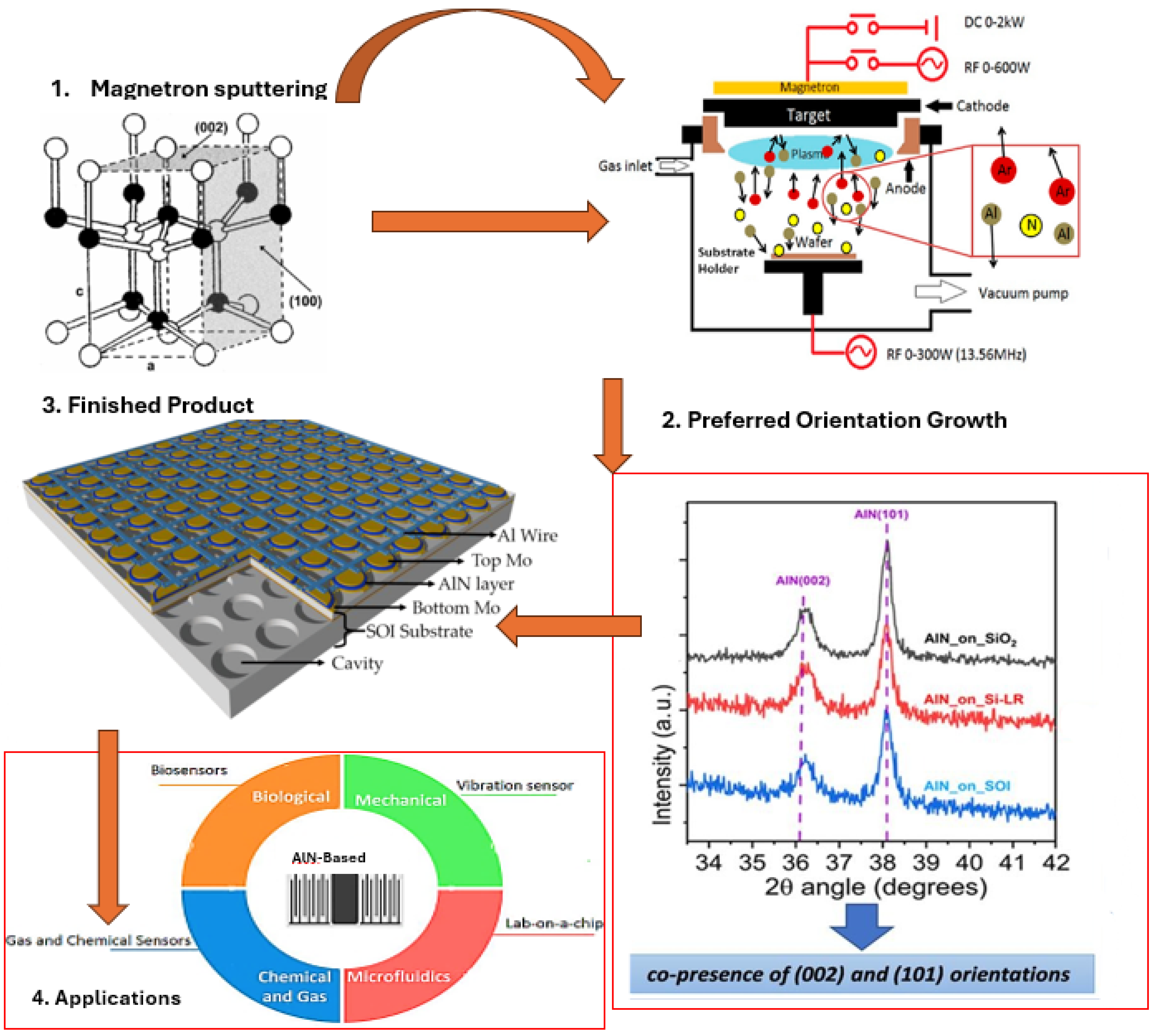
Figure 1. Summary of ALN-based thin-film fabrication process via magnetron sputtering. (1) Magnetron sputtering setup for AlN deposition, depicting plasma generation and target sputtering. The crystallographic planes (002) and (100) represent different orientations within the AlN crystal lattice. (2) X-ray diffraction (XRD) results showing preferred orientation growth, including peaks at AlN(002) and AlN(101), indicating the coexistence of these orientations on various substrates (SOI, Si-LR, SiO2). (3) Schematic of the fabricated device, comprising an SOI substrate, AlN layer, Mo electrodes (top and bottom), and an underlying cavity. (4) Overview of application areas for AlN-based devices, including biological sensors, mechanical sensors, chemical/gas sensors, microfluidics, and lab-on-a-chip technologies Images reproduced with permission [33,34,35,36].
Inorganics 12 00264 g001
Figure 2. (a) illustrates the hexagonal lattice structure and the a, c axes, which are parallel to planes (001) and (100), respectively, and (b) illustrates the covalent bond angle and length between Al, and N atoms and the tetrahedron structures [1].
Inorganics 12 00264 g002
Figure 3. Schematic of the magnetron sputtering process and the main system components for RF, DC, Pulsed DC, and HiPIM DC magnetron sputtering, recreated from [51].
Inorganics 12 00264 g003
Figure 4. Schematic of a planar magnetron discharge used in the magnetron sputtering processes, where the purple glow represents the plasma, with permission from [50].
Inorganics 12 00264 g004
Figure 5. Schematic of a rotating magnetron discharge used in the magnetron sputtering processes, where the purple glow represents the plasma, with permission from [50].
Inorganics 12 00264 g005
Figure 6. (af) AlN films with varied orientations for three samples alongside schematic morphology diagrams [61].
Inorganics 12 00264 g006
Figure 7. Collision probability vs. sputtering pressure for highly oriented AIN (100) thin film (reproduced from [1]).
Inorganics 12 00264 g007
Figure 8. Diagram illustrating the relationship between residual stress, crystalline quality, and deposition rate with respect to sputtering parameters [41].
Inorganics 12 00264 g008
Figure 9. (ad) AlN films grown at room temperature under various power levels: 300 W, 400 W, 500 W, and 600 W for abcd, respectively [64].
Inorganics 12 00264 g009
Figure 10. XRD pattern showing the AlN (002) and Mo(110) peaks for growth under a substrate temperature of 450 °C and a sputtering power of 8000 W [65].
Inorganics 12 00264 g010
Figure 11. Time-averaged ion energy distribution functions (IEDFs) obtained for (a) DC magnetron sputtering (DCMS) and (b) high-power impulse magnetron sputtering (HiPIMS) plasmas, as investigated by Jyotish Patidar et al. from [66].
Inorganics 12 00264 g011
Figure 12. Comparison of SEM images illustrating the grain distribution of AlN films that are: (a) undoped and (b) scandium-doped. Recreated from [71].
Inorganics 12 00264 g012
Figure 13. AlN−based cross-section of FBAR structure.
Inorganics 12 00264 g013
Figure 14. AlN-based energy harvester MEMS device showing layers of materials used, along with the variation in resistance, frequency of operation and output power. Reproduced from [79].
Inorganics 12 00264 g014
Table 1. Key points and parameters in AlN growth and mechanism.
Key Points/ParametersDescription
Crystal OrientationsAlN film growth primarily along the AlN(100) and AlN(001) planes determined by vibrational phonon modes.
Operational ParametersRF power, pressure, temperature, and target distance influence crystal orientation.
Deposition ProcessAdsorption, diffusion, nucleation, and coalescence form thin-film layers.
Processing ParametersKey for high-quality films, optimized via magnetron sputtering.
Nanostructure GrowthReactive magnetron sputtering enables tailored nanostructure growth.
Substrate InfluenceSubstrate material and morphology impact film properties.
Table 2. Comparison of different thin-film deposition techniques.
Deposition TechniqueSubstrate Temperature (°C)Growth Rate (Å/min)Film QualityEquipment ComplexityApplication Suitability
Reactive RF Magnetron Sputtering500–70010–20HighModerateLarge area, uniform films
DC Magnetron Sputtering500–70010–20ModerateLowConductive targets, large area
Dual Ion Beam Sputtering300–6005–15Very HighHighHigh-quality films, advanced electronics
Molecular Beam Epitaxy (MBE)650–8500.1–1Very HighVery HighHigh-purity single-crystal films
Chemical Vapor Deposition (CVD)600–9005–10HighHighLarge area, uniform films, electronic packaging
Pulsed Laser Deposition (PLD)500–7502-5HighModerateComplex material deposition, research applications
Disclaimer/Publisher’s Note: The statements, opinions and data contained in all publications are solely those of the individual author(s) and contributor(s) and not of MDPI and/or the editor(s). MDPI and/or the editor(s) disclaim responsibility for any injury to people or property resulting from any ideas, methods, instructions or products referred to in the content.