Article

Abnormal Fano Profile in Graphene-Wrapped Dielectric Particle Dimer

1
School of Science, Jiangsu Provincial Research Center of Light Industrial Optoelectronic Engineering and Technology, Jiangnan University, Wuxi 214122, China
2
Shandong Provincial Engineering and Technical Center of Light Manipulations & Shandong Provincial Key Laboratory of Optics and Photonic Device, School of Physics and Electronics, Shandong Normal University, Jinan 250014, China
*
Author to whom correspondence should be addressed.
Photonics 2020, 7(4), 124; https://doi.org/10.3390/photonics7040124
Submission received: 4 November 2020 / Revised: 30 November 2020 / Accepted: 2 December 2020 / Published: 3 December 2020
(This article belongs to the Special Issue Recent Advances in the Study of Light Propagation in Optical Fibers)

Abstract

:
We give a theoretical study on the near field enhancement and far field spectrum of an adjacent graphene-wrapped sphere dimer with different radii. The Fano profile is found in the near field enhancement spectrum of such a symmetry-broken dimer system, which is, however, hidden in the far field spectrum. We demonstrate that this kind of Fano profile is rising from the coupling of dimer’s plasmon hybridization modes by analyzing the dipole moments of each sphere. Moreover, different orientation of incident wave polarization will lead to the different plasmon hybridization coupling, thus giving rise to a different Fano profile. By changing the Fermi energy level, we could achieve tunable Fano profile in near field enhancement.

Graphical Abstract

1. Introduction

As a promising plasmonic materials, graphene has unique optical and electronic properties due to its high electron mobility, unique field enhancement by the plasmons in THz [1,2,3,4,5] as well as nonlinearity [6,7,8,9], so that it has potential applications in modulators [10,11], optical sensing, polarizers, mid-infrared photodetectors [5,12]. The plasmonic property of the graphene layer is comparable to that of thin metal sheets with the thickness of tens of nanometers [13]. In comparison with surface plasmon on a metal–dielectric interface, the graphene’s plasmon is more superior due to the strong confinement of electromagnetic energy [14]. The high-sensitivity tunable plasmonic biosensor has been demonstrated, and the spatial light confinement in graphene is up to two orders of magnitude higher than that in metals [15]. The multi-band perfect plasmonic absorptions have been achieved in single-layer graphene-based rectangular gratings via the excitation of standing-wave graphene surface plasmon polaritons [16].
On the other hand, coupled plasmonic nano-elements (nanoparticle or nanocrystal) attract more and more attention due to the new freedom of operation of localized surface plasmon resonances [17,18]. The coupling of nano-element plasmons could not only dramatically shift the spectrum and increase the field enhancement, but also cause new plasmon modes [19]. Therefore, these coupled nano-elements have a lot of potential applications in sensing [20], Raman spectroscopy [21,22], optical switches [23], optical tweezers [24], and meta-lenses [25]. Such kinds of plasmonic coupled hybridized nano-elements could form the basic uni-cell to support many functional devices. Actually, graphene-based coupled plasmonic structure could benefit from the advantages of both superior plasmons in THz and new coupled plasmon modes. In many previous studies, graphene acts as a 2D material due to its nature geometric property. Few works are aimed to investigate the 3D graphene-based structure [26,27,28,29]. In this paper, we aim to study the near field and far field property of a novel adjacent 3D graphene-wrapped spheres dimer in which the spheres have different radii. Based on the dipole–dipole approximation, we demonstrate that the different coupling modes of the dimer will lead to different Fano profiles in their near field enhancement spectrum, and this kind of Fano profile will be generally hidden in the far-field spectrum.

2. Materials and Methods

We consider the dielectric dimer with permittivity ε covered by graphene layer, as shown in Figure 1. In experiment, the graphene-wrapped spheres can be obtained by using layer-by-layer self-assembly or precursor-assisted chemical vapor deposition [30,31,32]. Assuming the electric displacement vector D n inside ( n = c ) and outside ( n = h ) the sphere have linear relation with the electric field E n , i.e., D n = ε n E n . In the case r 1 and r 2 are far less than the wavelength of the incident light, we can adopt the so-called quasi-static approximation. Hence, the electric potentials both inside and outside a single spherical particle would satisfy the Laplace equation: 2 φ n = 0 . Under the linearly polarized plane wave illumination, the general solutions of the Laplace equations would be written as
φ c = B E 0 r cos θ , φ h = E 0 ( r C r 2 ) cos θ .
The electric potential inside the particle includes the incident part and the induced one, i.e., E i + E i n d = φ c . As to φ h , we have E i + E s = φ h , in which E s is the scattering field in the host. E 0 is the amplitude of the external applied field, and B , C are the unknown coefficients to be determined. For the monolayer graphene coated dielectric sphere in which graphene layer is considered as an extremely thin conducting shell with conductivity σ , due to the fact that the thickness of monolayer graphene is much smaller than the dielectric core. Generally, zone folding for planar graphene quantizes the allowable electronic momenta and hence modifies the linear energy dispersion. However, these perturbations incur only negligible changes to the conductive response provided the inverse circumference remains small relative to the Fermi momentum [26]. Therefore, the graphene coating could be characterized well as a two-dimension homogenized conducting film, as we will show below. We introduce the non-source-free boundary conditions [27],
n ^ × E i + E s E i + E i n d r = r 1 , r 2 = 0 , n ^ D i + D s D i + D i n d r = r 1 , r 2 = ρ ,
where ρ is the surface density of charge, which has relation s j / / = i ω ρ with surface density of linear current j / / at the frequency ω . Here, the operator s stands for surface divergence, and j / / = σ E / / with the tangential field component E / / of the induced field and the surface conductivity σ .
Solving the above equations, we yield the unknown coefficients for each single particle,
B 1 , 2 = 3 ε h ε + 2 ε h + 2 Θ 1 , 2 , C 1 , 2 = ε ε h + 2 Θ 1 , 2 ε + 2 ε h + 2 Θ 1 , 2 r 1 , 2 3 ,
where Θ 1 , 2 = i σ / ω r 1 , 2 ε 0 and the effective polarizability for the graphene-wrapped dielectric particle would be,
α 1 , 2 = 4 π C 1 , 2 .
The subscript 1,2 denotes that for particle 1 or 2. Next, to consider the particle–particle interaction, two particles are modeled as point dipoles with the present effective polarizability in dipole–dipole limit. The external field along with the incident field at each particle positions satisfy the following equations,
E 1 = 1 α 2 A 12 1 α 1 α 2 A 12 A 21 E 0 , E 2 = 1 α 1 A 21 1 α 1 α 2 A 12 A 21 E 0 ,
where A 12 = A 21 = e i k d 2 π i k d 2 1 d 3 denoting the dipole–dipole interaction factor, and k is the wave vector in the host medium. The dipole moments for each particle are thus given by,
p 1 , 2 = ε 0 α 1 , 2 E 1 , 2
The term α 1 α 2 A 12 A 21 shows the dipole–dipole interaction strength of the two coupled particles. The internal field in each graphene-wrapped particle will be
E i n 1 , 2 = B 1 , 2 E 1 , 2 .
To model the surface conductivity of the graphene, we introduce the simplified linear version within the random-phase approximation in THz frequencies [33]
σ = σ i n t r a + σ i n t e r .
where σ i n t r a and σ i n t e r are the intraband and interband terms, which have the following forms
σ i n t r a = i e 2 k B T π ħ 2 ( ω + i / τ ) E F k B T + 2 ln ( e E F k B T + 1 ) , σ i n t e r = i e 2 4 π ħ ln 2 E F ( ω + i τ 1 ) ħ 2 E F + ( ω + i τ 1 ) ħ .
where E F = ħ ν F ( π n 2 D ) 1 / 2 is the Fermi energy, which can be electrically controlled by an applied gate voltage due to the strong dependence of the carrier density n 2 D on the gate voltage, τ is the electron–phonon relaxation time, and T is the temperature in K . e , ħ , k B , and ν F are the electron charge, reduced Planck’s constant, Boltzmann constant, and the Fermi velocity of electrons, respectively. In the case of frequencies 2 E F > ħ ω , σ σ i n t r a because the interband transitions in graphene are forbidden by Pauli exclusion principle. Additionally, E F k B T in the room temperature ( T = 300   K ), the linear surface conductivity reduced to a simplified version as
σ 0 = i e 2 π ħ E F ħ ω + i τ 1 .
To investigate the far field properties, we give the general expression for the extinction cross-sections (ECS) of adjacent graphene-wrapped dielectric dimer with dipole moments and incident fields as
σ e x t = i = 1 2 k ε 0 E 0 2 Im E 0 , i * p i ,
and total absorption cross-sections (ACS) for the dimer is the linear combination of all contributions from two particles, which has the following expression
σ a b s = i = 1 2 k ε 0 E 0 2 k 3 6 π p i 2 Im p i 2 α i .

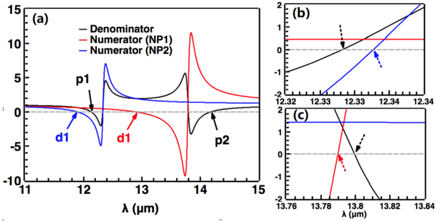
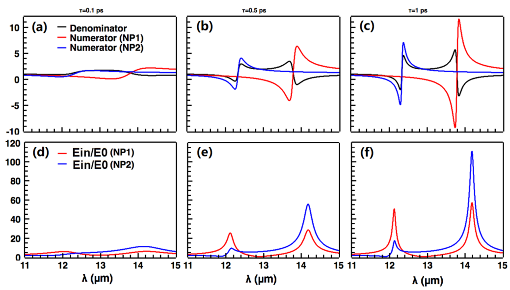
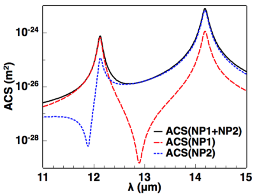
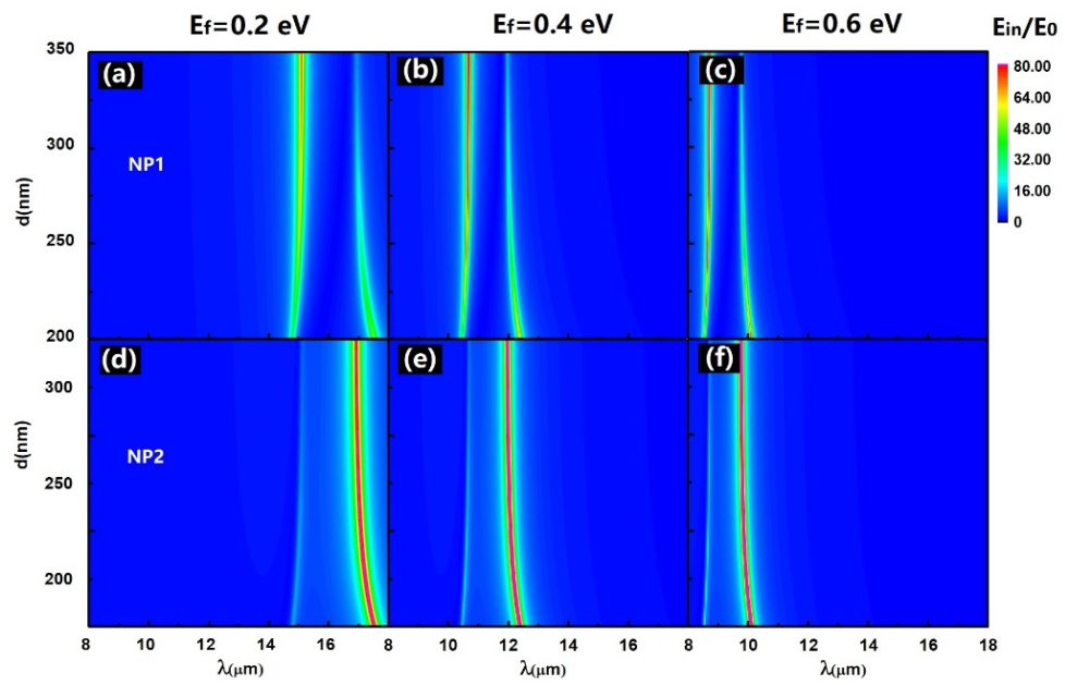
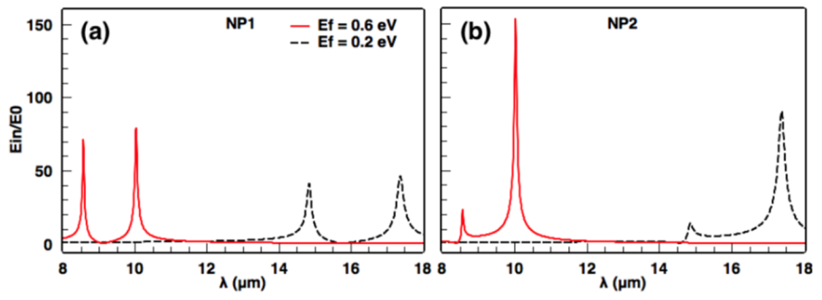
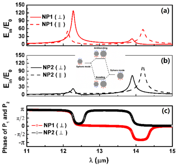
3. Results and Discussion

In Figure 2, we plot internal field enhancement for the proposed graphene-wrapped dielectric dimers with various geometry parameters at a fixed center-to-center separation d = 210   nm in THz frequency. The dielectric core is chosen as silica with the dielectric constant ε = 2.25 . The radii of small particle vary from 50 to 80 nm, and the large one is kept constant at 100 nm. As the small particle (NP1) grows, the internal field enhancement spectra for each particle show additional peaks indicating strong interaction between the graphene-wrapped dimer particles, and these additional resonant peaks dominate with stronger particle–particle interaction. Compared to the single particle case (see the dotted lines in Figure 2), the main peaks of the internal field enhancement curves for two particle have different shifting behaviors: NP1 illustrates blue-shifting along with magnitude dramatically decreasing, and NP2 shows red-shifting with peak magnitude slightly growing. For details, the main peak wavelength and corresponding magnitudes are listed as follows: 9.74   μ m   123.6 , 10.65   μ m 102.5 , 11.45   μ m 79.1 , and 12.12   μ m 50.5 for NP1; 13.84   μ m   100.2 , 13.89   μ m 103.4 13.99   μ m 107.7 , and 14.19   μ m 110.7 for NP2. It demonstrated that the dipole–dipole interaction will reduce internal field in small particle and enhance the field inside the large particle in the main peak near their individual resonant wavelength.
Note that additional resonant peaks in field enhancement spectra are due to the particle–particle interaction, however they arise from different origins. We plot the phase spectra for NP1 and NP2 in Figure 2. Dipole moments of NP1 and NP2 are in-phase in resonant peak at long wavelength ( λ 14   μ m , see Figure 2IV(c)), so that the peak for both particles are dramatically enhanced when the particle–particle interaction becomes strong. In this case, not only NP1 but also NP2 benefit from the particle–particle coupling. On the other hand, NP1 and NP2 are out-of-phase at a short wavelength (see Figure 2IV(c)), hence field enhancement is eliminated for NP1 and additional resonant peak in NP2 shows less dominating. These “in-phase” and “out-of-phase” coupling modes result from the so-called cascaded plasmon resonances [34,35] in adjacent nanoparticles with different radii, as indicated schematically in the inset in Figure 2IV(b). Alternately, they are relevant to “bonding” and “anti-bonding” modes due to the different coupling symmetry of charge distributed around two adjacent particles. Similar to the plasmon hybridization of metallic shell [19], we introduce the hybridization theory to explain the two resonant modes in the cascaded dimer, of which schematic diagram is shown in Figure 3. Besides that, the sharp anti-bonding mode interferes with the relatively broadband bonding mode thus leads to a well-pronounced asymmetric sharp line profile–Fano resonant profile in the internal field enhancement spectra for NP2 (see the middle panels in Figure 2). Additionally, the Fano curve becomes obvious as the coupling strength grows. However, no Fano profile exists in NP1’s internal field enhancement spectra. This kind of Fano profile is different from the coupling of optical excitations existing in different materials, for instance, a silver-gold heterogeneous dimer, whose Fano profile is arising from the coupling of localized surface plasmon resonance of silver component and the continuum of interband transitions of the gold one [36,37,38,39]. To further illustrate, we start next with the mathematical analysis.
In Equation (5), the numerator term 1 α 1 A 21 (or 1 α 2 A 12 ) and denominator term 1 α 1 α 2 A 12 A 21 are both convergent, thus the resonant peak will mathematically occur when 1 α 1 α 2 A 12 A 21 = 0 , and the resonant dip will consequently show when 1 α 1 A 21 = 0 . We calculate the denominator and numerator terms within the present model in Figure 4a, and it illustrates the two main resonant peaks (denoted as points p1 and p2 in Figure 4a) in the near field enhancement spectrum of NP1 and NP2. Point d1(blue) indicates the Fano dip of the antibonding mode for NP2. Although there is no obvious Fano profile in the near field spectrum of NP1, numerator term 1 α 1 A 21 has zero value in the spectrum, which is denoted as d1(red). Calculation results show that the zero point d1(red) varies with the particle geometric parameters; for instance, for particle radius and particle–particle distance, it indicates less dependence on the p1 point, so that no obvious Fano-like curve exists in the position of anti-bonding mode in NP1’s near field spectrum, especially when the particle-particle interaction is weak. However, d1(blue) goes together with p1, therefore the Fano curve keeps well in NP2’s near field spectrum no matter how the geometric parameter changes. It is easy to understand that the dipole excitation of NP1 predominates in the existence of antibonding mode for both NP1 and NP2, as to the internal field enhancement its self, antibonding coupling has less influence on the near field in NP1 than that in NP2, so that the Fano profile is not obvious in NP1 especially when the particle–particle interaction is weak. Once the coupling strength becomes strong, we will see a slight “zero dip” in Figure 2IV(a). For NP2, internal field enhancement mainly relies on antibonding coupling, hence the Fano profile keeps well.
Besides the “zero points” remarked in Figure 4a, there exists other ones at the very narrow band spectrum around 12.3   μ m and 13.8   μ m . It is clearly shown in Figure 4b,c that the “zero points” of denominator and numerator are not located exactly at the same position where it is expected to exhibit Fano profile. However, due to the retarded effects resulting from the electron damping in graphene layer, no Fano curve occurs. To further demonstrate, we investigate influence of the electron relaxation times on the near field Fano profile in Figure 5. It clearly shows that the peaks of Fano curves have been eliminated with very short relaxation time in the graphene layer.
The sharp anti-bonding mode interferes with the relatively broadband bonding mode, thus leading to a sharp Fano resonant profile in internal field enhancement spectra for NP2 (see the middle panels in Figure 2). Additionally, the Fano curve becomes obvious as the coupling strength grows. However, this intrinsic Fano resonance existing in near field might be hidden in the curve of the far field spectrum. To demonstrate, we plot the extinction cross-section spectrum (ECS) in Figure 6 according to the general expression for the extinction cross-sections of adjacent particles with dipole moments and incident field as follow in Equation (11). As Equation (11) contains two separated terms corresponding to NP1 and NP2, respectively, which indicate different contributions of adjacent dimer to the total ECS, we separate the two different contributions accordingly in Figure 6. It is clearly shown that the ECS curves are typically symmetric line shape for both total and separate contributions. The opposite sign of separate ECS in the antibonding resonance demonstrates the different contributions of the adjacent dimer to the total ECS especially for NP2. The negative value of ECS means the enhanced forward light passing by the particle along the incident direction, which is abnormal for a lossy particle. The particle–particle interaction in the adjacent dimer leads to the enhanced forward light for NP2 (with negative ECS value 0.072   μ m 2 ) but more extinct forward light for NP1 (with positive ECS value 0.158   μ m 2 ) so that the total ECS still keeps positive.
The situation is similar in the total absorption cross-section as shown in Figure 7. The total absorption cross-section (ACS) for the dimer is defined in Equation (12). Contrary to the total ACS, the separate contributions of NP1 and NP2 show asymmetric Fano profiles in the ACS curves around anti bonding position, respectively. Unlike the separate contributions in the ECS, the separate terms in Equation (12) are more relative to the dipole moments itself, so that the line shape is similar to the internal field showing the Fano profile.
Figure 8 illustrates the dependence of internal field enhancements on particle distance and Fermi energy level. Tuning the density of the charge carriers through the external electrical gating field or chemical doping will result in the changing of Fermi level of the graphene covering, thus altering the surface plasmon resonance of the particle dimmer. Blue shift of the resonant peaks occurs with the increase in the Fermi energy level, which was concluded in other similar structures [28]. Besides the blue-shift resonances, higher Fermi energy level leads to the stronger internal field intensities both in NP1 and NP2, as showed in Figure 9 for a clear view. It is shown that when E F = 0.2   eV , resonant wavelengths for both NP1 and NP2 lay at 14.86   μ m and 17.38   μ m with peak values 41.18 and 46.45 for NP1, and with 14.08 and 90.57 for NP2. Once E F is increased to 0.6   eV , then we yield the resonant wavelengths and corresponding peak values as follows: 8.57   μ m   71.77 and 10.04 μ m   79.17 for NP1; 8.57   μ m   23.58 and 1.
Up to now, we analyze the near field enhancement and far field properties of adjacent graphene dimer under linearly polarized light illumination with the polarization direction parallel to the dimer axis. In this case, “out-of-phase” anti-bonding and “in-phase” bonding modes are excited according to the plasmon hybridization model. Note that such a plasmonic dimer structure shall generally predict four plasmon hybridization formations within the dipole approximation [18,40,41], which corresponds to different orientation of exciting incident polarization. If the polarization direction is perpendicular to the dimer axis, paralleled dipole moments of NP1 and NP2 exhibit “in-phase” anti-bonding mode and “out-of-phase” bonding mode. Additionally, the “in-phase” anti-bonding mode has higher energy than the “out-of-phase” bonding one, as shown in Figure 10. Although the coupling strength of plasmon hybridization in this situation is weaker, the Fano profile in the near field enhancement still exists.
In the end, we should mark that the full wave numerical approach [36,37,38] will give more accurate description of near field and far field response due to the plasmons in the dimer system, especially for the dimer system with the dimension not smaller enough to the incident wavelength. In the present model, we learn, on one hand, that the size of the particle is about one tenth of the incident wavelength, hence the dipole excitation of the particle plays the dominating role in the plasmonic resonances, and the influence of the other higher order mode can be neglected. On the other hand, physically, the Fano profile here arises from the coupling of the dipole modes. Consequently, the conclusion we made with the dipole–dipole approach will stay the same with that obtained by a more accurate numerical approach, except for some very limited deviation (that could be neglected) in the near field and far field configurations.

4. Conclusions

In summary, with a dipole–dipole approximation, we investigate the near field enhancement and far field property of a graphene-wrapped sphere dimer. When the graphene-wrapped sphere in dimer has different radius, the symmetry of the dimer system is broken, and the Fano profile arises in the near field enhancement spectrum. This Fano profile is due to the coupling of the bonding and antibonding mode of the dimer’s plasmon hybridization and is sensitive to the sphere whose individual plasmon give more contribution to the bonding mode. We fix the Fano dip with mathematical analysis and find that the relaxation time play the role in the appearance of the Fano profile. In the far field spectrum, however, no Fano profile occurs neither in extinction cross-section nor in the overall absorption cross-section spectrum. The Fano profile in the near field could be tuned by variable Fermi energy levels both in resonant wavelength and amplitude of peak value. In the end, we show that different orientation of polarization direction of incident waves corresponding to the dimer axis will cause different plasmon hybridization coupling; then, the position of the Fano profile will be different.

Author Contributions

Conceptualization, Y.H. and P.M.; methodology, Y.H.; formal analysis, Y.H.; investigation, Y.H.; writing—original draft preparation, Y.H.; writing—review and editing, Y.H., P.M., and Y.M.W. All authors have read and agreed to the published version of the manuscript.

Funding

This research was funded by the National Natural Science Foundation of China grant number 11704158 and 12004225, the Natural Science Foundation of Jiangsu Province grant number BK20170170, and China Postdoctoral Science Foundation grant number 2020M672112.

Conflicts of Interest

The authors declare no conflict of interest.

References

  1. Koppens, F.H.L.; Chang, D.E.; García de Abajo, F.J. Graphene Plasmonics: A Platform for Strong Light–Matter Interactions. Nano Lett. 2011, 11, 3370–3377. [Google Scholar] [CrossRef] [PubMed] [Green Version]
  2. Ju, L.; Geng, B.; Horng, J.; Girit, C.; Martin, M.; Hao, Z.; Bechtel, H.A.; Liang, X.; Zettl, A.; Shen, Y.R.; et al. Graphene plasmonics for tunable terahertz metamaterials. Nat. Nanotechnol. 2011, 6, 630–634. [Google Scholar] [CrossRef] [PubMed]
  3. Grigorenko, A.N.; Polini, M.; Novoselov, K.S. Graphene plasmonics. Nat. Photonics 2012, 6, 749–758. [Google Scholar] [CrossRef]
  4. Brar, V.W.; Jang, M.S.; Sherrott, M.; Lopez, J.J.; Atwater, H.A. Highly Confined Tunable Mid-Infrared Plasmonics in Graphene Nanoresonators. Nano Lett. 2013, 13, 2541–2547. [Google Scholar] [CrossRef] [PubMed] [Green Version]
  5. Low, T.; Avouris, P. Graphene Plasmonics for Terahertz to Mid-Infrared Applications. ACS Nano 2014, 8, 1086–1101. [Google Scholar] [CrossRef] [PubMed] [Green Version]
  6. Hendry, E.; Hale, P.J.; Moger, J.; Savchenko, A.K.; Mikhailov, S.A. Coherent Nonlinear Optical Response of Graphene. Phys. Rev. Lett. 2010, 105, 097401. [Google Scholar] [CrossRef] [PubMed] [Green Version]
  7. Constant, T.J.; Hornett, S.M.; Chang, D.E.; Hendry, E. All-optical generation of surface plasmons in graphene. Nat. Phys. 2016, 12, 124–127. [Google Scholar] [CrossRef] [Green Version]
  8. Jiang, T.; Huang, D.; Cheng, J.; Fan, X.; Zhang, Z.; Shan, Y.; Yi, Y.; Dai, Y.; Shi, L.; Liu, K.; et al. Gate-tunable third-order nonlinear optical response of massless Dirac fermions in graphene. Nat. Photonics 2018, 12, 430–436. [Google Scholar] [CrossRef] [Green Version]
  9. Soavi, G.; Wang, G.; Rostami, H.; Purdie, D.G.; De Fazio, D.; Ma, T.; Luo, B.; Wang, J.; Ott, A.K.; Yoon, D.; et al. Broadband, electrically tunable third-harmonic generation in graphene. Nat. Nanotechnol. 2018, 13, 583–588. [Google Scholar] [CrossRef] [Green Version]
  10. Ansell, D.; Radko, I.P.; Han, Z.; Rodriguez, F.J.; Bozhevolnyi, S.I.; Grigorenko, A.N. Hybrid graphene plasmonic waveguide modulators. Nat. Commun. 2015, 6, 8846. [Google Scholar] [CrossRef]
  11. Brar, V.W.; Sherrott, M.C.; Jang, M.S.; Kim, S.; Kim, L.; Choi, M.; Sweatlock, L.A.; Atwater, H.A. Electronic modulation of infrared radiation in graphene plasmonic resonators. Nat. Commun. 2015, 6, 7032. [Google Scholar] [CrossRef] [PubMed]
  12. García de Abajo, F.J. Graphene Plasmonics: Challenges and Opportunities. ACS Photonics 2014, 1, 135–152. [Google Scholar] [CrossRef] [Green Version]
  13. He, X.; Gao, P.; Shi, W. A further comparison of graphene and thin metal layers for plasmonics. Nanoscale 2016, 8, 10388–10397. [Google Scholar] [CrossRef] [PubMed]
  14. Jablan, M.; Soljacic, M.; Buljan, H. Plasmons in Graphene: Fundamental Properties and Potential Applications. Proc. IEEE 2013, 101, 1689–1704. [Google Scholar] [CrossRef]
  15. Rodrigo, D.; Limaj, O.; Janner, D.; Etezadi, D.; Garcia de Abajo, F.J.; Pruneri, V.; Altug, H. Mid-infrared plasmonic biosensing with graphene. Science 2015, 349, 165–168. [Google Scholar] [CrossRef] [Green Version]
  16. Xia, S.-X.; Zhai, X.; Huang, Y.; Liu, J.-Q.; Wang, L.-L.; Wen, S.-C. Multi-band perfect plasmonic absorptions using rectangular graphene gratings. Opt. Lett. 2017, 42, 3052. [Google Scholar] [CrossRef]
  17. Halas, N.J.; Lal, S.; Chang, W.-S.; Link, S.; Nordlander, P. Plasmons in Strongly Coupled Metallic Nanostructures. Chem. Rev. 2011, 111, 3913–3961. [Google Scholar] [CrossRef]
  18. Deng, T.-S.; Parker, J.; Yifat, Y.; Shepherd, N.; Scherer, N.F. Dark Plasmon Modes in Symmetric Gold Nanoparticle Dimers Illuminated by Focused Cylindrical Vector Beams. J. Phys. Chem. C 2018, 122, 27662–27672. [Google Scholar] [CrossRef]
  19. Prodan, E. A Hybridization Model for the Plasmon Response of Complex Nanostructures. Science 2003, 302, 419–422. [Google Scholar] [CrossRef]
  20. Willets, K.A.; Van Duyne, R.P. Localized Surface Plasmon Resonance Spectroscopy and Sensing. Annu. Rev. Phys. Chem. 2007, 58, 267–297. [Google Scholar] [CrossRef] [Green Version]
  21. Lim, D.-K.; Jeon, K.-S.; Kim, H.M.; Nam, J.-M.; Suh, Y.D. Nanogap-engineerable Raman-active nanodumbbells for single-molecule detection. Nat. Mater. 2010, 9, 60–67. [Google Scholar] [CrossRef]
  22. Arroyo, J.O.; Kukura, P. Non-fluorescent schemes for single-molecule detection, imaging and spectroscopy. Nat. Photonics 2016, 10, 11–17. [Google Scholar] [CrossRef]
  23. Large, N.; Abb, M.; Aizpurua, J.; Muskens, O.L. Photoconductively Loaded Plasmonic Nanoantenna as Building Block for Ultracompact Optical Switches. Nano Lett. 2010, 10, 1741–1746. [Google Scholar] [CrossRef] [PubMed] [Green Version]
  24. Grigorenko, A.N.; Roberts, N.W.; Dickinson, M.R.; Zhang, Y. Nanometric optical tweezers based on nanostructured substrates. Nat. Photonics 2008, 2, 365–370. [Google Scholar] [CrossRef] [Green Version]
  25. Kawata, S.; Ono, A.; Verma, P. Subwavelength colour imaging with a metallic nanolens. Nat. Photonics 2008, 2, 438–442. [Google Scholar] [CrossRef]
  26. Christensen, T.; Jauho, A.-P.; Wubs, M.; Mortensen, N.A. Localized plasmons in graphene-coated nanospheres. Phys. Rev. B 2015, 91, 125414. [Google Scholar] [CrossRef] [Green Version]
  27. Smirnova, D.A.; Shadrivov, I.V.; Miroshnichenko, A.E.; Smirnov, A.I.; Kivshar, Y.S. Second-harmonic generation by a graphene nanoparticle. Phys. Rev. B 2014, 90. [Google Scholar] [CrossRef] [Green Version]
  28. Huang, Y.; Miroshnichenko, A.E.; Gao, L. Low-threshold optical bistability of graphene-wrapped dielectric composite. Sci. Rep. 2016, 6, 23354. [Google Scholar] [CrossRef] [Green Version]
  29. Zhang, K.; Huang, Y.; Miroshnichenko, A.E.; Gao, L. Tunable Optical Bistability and Tristability in Nonlinear Graphene-Wrapped Nanospheres. J. Phys. Chem. C 2017, 121, 11804–11810. [Google Scholar] [CrossRef]
  30. Lee, J.S.; You, K.H.; Park, C.B. Highly Photoactive, Low Bandgap TiO2 Nanoparticles Wrapped by Graphene. Adv. Mater. 2012, 24, 1133. [Google Scholar] [CrossRef]
  31. Lee, J.-S.; Kim, S.-I.; Yoon, J.-C.; Jang, J.-H. Chemical Vapor Deposition of Mesoporous Graphene Nanoballs for Supercapacitor. ACS Nano 2013, 7, 6047–6055. [Google Scholar] [CrossRef] [PubMed]
  32. Wu, P.; Wang, H.; Tang, Y.; Zhou, Y.; Lu, T. Three-Dimensional Interconnected Network of Graphene-Wrapped Porous Silicon Spheres: In Situ Magnesiothermic-Reduction Synthesis and Enhanced Lithium-Storage Capabilities. ACS Appl. Mater. Interfaces 2014, 6, 3546–3552. [Google Scholar] [CrossRef] [PubMed]
  33. Dai, X.; Jiang, L.; Xiang, Y. Tunable optical bistability of dielectric/nonlinear graphene/dielectric heterostructures. Opt. Express 2015, 23, 6497. [Google Scholar] [CrossRef] [PubMed]
  34. Li, K.; Stockman, M.I.; Bergman, D.J. Self-Similar Chain of Metal Nanospheres as an Efficient Nanolens. Phys. Rev. Lett. 2003, 91. [Google Scholar] [CrossRef] [PubMed]
  35. Toroghi, S.; Kik, P.G. Cascaded plasmon resonant field enhancement in nanoparticle dimers in the point dipole limit. Appl. Phys. Lett. 2012, 100, 183105. [Google Scholar] [CrossRef] [Green Version]
  36. Bachelier, G.; Russier-Antoine, I.; Benichou, E.; Jonin, C.; Del Fatti, N.; Vallée, F.; Brevet, P.-F. Fano Profiles Induced by Near-Field Coupling in Heterogeneous Dimers of Gold and Silver Nanoparticles. Phys. Rev. Lett. 2008, 101, 197401. [Google Scholar] [CrossRef]
  37. Yang, Z.-J.; Zhang, Z.-S.; Zhang, W.; Hao, Z.-H.; Wang, Q.-Q. Twinned Fano interferences induced by hybridized plasmons in Au–Ag nanorod heterodimers. Appl. Phys. Lett. 2010, 96, 131113. [Google Scholar] [CrossRef]
  38. Lombardi, A.; Grzelczak, M.P.; Pertreux, E.; Crut, A.; Maioli, P.; Pastoriza-Santos, I.; Liz-Marzán, L.M.; Vallée, F.; Del Fatti, N. Fano Interference in the Optical Absorption of an Individual Gold–Silver Nanodimer. Nano Lett. 2016, 16, 6311–6316. [Google Scholar] [CrossRef] [Green Version]
  39. Ávalos-Ovando, O.; Besteiro, L.V.; Wang, Z.; Govorov, A.O. Temporal plasmonics: Fano and Rabi regimes in the time domain in metal nanostructures. Nanophotonics 2020, 9, 3587–3595. [Google Scholar] [CrossRef]
  40. Brown, L.V.; Sobhani, H.; Lassiter, J.B.; Nordlander, P.; Halas, N.J. Heterodimers: Plasmonic Properties of Mismatched Nanoparticle Pairs. ACS Nano 2010, 4, 819–832. [Google Scholar] [CrossRef]
  41. Sheikholeslami, S.; Jun, Y.; Jain, P.K.; Alivisatos, A.P. Coupling of Optical Resonances in a Compositionally Asymmetric Plasmonic Nanoparticle Dimer. Nano Lett. 2010, 10, 2655–2660. [Google Scholar] [CrossRef] [PubMed]
Figure 1. Schematic diagram of the graphene-wrapped dielectric dimer in vacuum illuminated by the linear polarized light whose E direction is along the dimer axis. The radii of two particles are r 1 and r 2 , respectively, and the center-to-center distance is d .
Photonics 07 00124 g001
Figure 2. Internal field enhancement spectra for graphene-wrapped dielectric dimers with constant center-to-center distance of d = 210 nm , for small particle (NP1, upper panels) and the large particle (NP2, middle panels) with various radii of small particle (I) r 1 = 50   nm , (II) r 1 = 60   nm , (III) r 1 = 70   nm , and (IV) r 1 = 80   nm , and with a fixed radius of large particle r 2 = 100   nm . The dashed line in each panel shows the analytical single particle field enhancement. Down panels illustrate the phase of each dipole moments in dimer calculated by Equation (6). The host medium is chosen as vacuum, ε = 2.25 , E F = 0.3   eV , and τ = 1   ps .
Photonics 07 00124 g002
Figure 3. The schematic diagram of the plasmon hybridization in the cascaded graphene-coated dimer. The Fano resonance arises due to the interference between antibonding and bonding modes.
Photonics 07 00124 g003
Figure 4. (a) Calculated results of denominator term 1 α 1 α 2 A 12 A 21 (black) and numerator terms 1 α 2 , 1 A 12 , 21 (red for NP1 and blue for NP2) in the function of incident wavelength. (b,c) are the local enlarged images cut from (a), located around 12.3   μ m and 13.8   μ m , respectively. The physical parameters used in the calculation are the same as in Figure 2IV.
Photonics 07 00124 g004
Figure 5. The same as in Figure 4 but with different relaxation times: (a) τ = 0.1   ps , (b) τ = 0.5   ps , (c) τ = 1   ps . Corresponding internal field enhancements are shown in (df), respectively.
Photonics 07 00124 g005
Figure 6. Extinction cross-section spectrum of total (black solid), NP1 (red dashed), and NP2 (blue dotted) contributions from the graphene-wrapped dimer.
Photonics 07 00124 g006
Figure 7. Absorption cross-section spectrum of total (black solid), NP1 (red dashed), and NP2 (blue dotted) contributions from the graphene-wrapped dimer, respectively.
Photonics 07 00124 g007
Figure 8. Internal field enhancement as the functions of center-to-center distance d and incident wavelength λ in NP1 (Upper panel) and NP2 (lower panel) with different Fermi energy levels: (a,d) E F = 0.2   eV , (b,e) E F = 0.4   eV , and (c,f) E F = 0.6   eV , respectively. The radius of NP1 is 80   nm and other parameters are the same as used in Figure 2.
Photonics 07 00124 g008
Figure 9. Internal field enhancement spectra with different Fermi energy levels in (a) NP1 and (b) NP2, respectively. Other geometric parameters are the same as in Figure 2IV.
Photonics 07 00124 g009
Figure 10. Internal field enhancement spectra in (a) NP1 and (b) NP2 with different polarization direction of incident wave: E perpendicular to dimer axis (solid) and E parallel to dimer axis (dashed). (c) Phase of the dipole moments for NP1 and NP2 in case of E perpendicular to dimer axis. Other physical parameters are the same as in Figure 2IV. The insert denotes the plasmon hybridization.
Photonics 07 00124 g010
Publisher’s Note: MDPI stays neutral with regard to jurisdictional claims in published maps and institutional affiliations.

