Article

Output Power Monitoring of Ultraviolet Light-Emitting Diode via Sapphire Substrate

1
Department of Electronic and Computer Engineering, National Taiwan University of Science and Technology, Taipei 106, Taiwan
2
Graduate Institute of Electro-Optical Engineering, National Taiwan University of Science and Technology, Taipei 106, Taiwan
*
Author to whom correspondence should be addressed.
Photonics 2020, 7(3), 63; https://doi.org/10.3390/photonics7030063
Submission received: 23 July 2020 / Revised: 23 August 2020 / Accepted: 24 August 2020 / Published: 25 August 2020
(This article belongs to the Section Lasers, Light Sources and Sensors)

Abstract

:
Ultraviolet (UV) light plays an important role in air/water/surface sterilization now. Maintaining a certain light intensity is often required to attain the targeted effect. In this paper, on-chip power monitoring of a UV-A light-emitting diode (LED) via sapphire substrate is reported. A p–i–n photodiode loop that surrounds the UV-A LED was designed and fabricated to monitor the output power by detecting the scattered light of the LED propagating through the sapphire substrate. No particular waveguide structure or processing parameter control was needed. The monitoring responsivities per unit of surface-emitting power obtained were approximately 21 and 25 mA/W at photodiode biases of 0 and 3 V, respectively. When combined with a transimpedance amplifier, a monitoring responsivity of 1.87 V/mW at zero bias was measured, and a different monitoring responsivity could be customized by adjusting the gain of the transimpedance amplifier. The operation principle of this device might be applicable to UV-B or UV-C LEDs.

Graphical Abstract

1. Introduction

Ultraviolet (UV) light-emitting diodes (LEDs) are used in various fields, such as for epoxy curing, air/water sterilization, and surface disinfection. Because the effectiveness of these applications depends on a minimum UV light intensity, the appropriate monitoring of in situ optical power is essential, particularly because AlGaN-based UV LEDs have a shorter lifetime than InGaN-based visible LEDs have. An external Si or InGaAs photodiode is often placed near the rear facet of a laser diode (LD) in commercial edge-emitting infrared LDs to monitor the output power level. Typically, surface-emitting LEDs do not exhibit strong lateral confinement on photons. On-chip power monitoring can be achieved by using the same active layer for both emission and detection under forward and reverse biases, respectively. Nevertheless, its responsivity is fairly low because the emission wavelength of the LED is near the cutoff wavelength of the photodiode. Tchernycheva et al. reported the integration of GaN-based single-wire LEDs and photodetectors optically coupled with silicon nitride waveguides [1]. Jiang et al. monolithically integrated blue LEDs and UV Schottky barrier photodiodes for bidirectional optical communication [2]. Li et al. reported the phenomenon of optical crosstalk in GaN-on-sapphire LEDs [3,4], and the monolithic integration of photodiodes, LEDs, and waveguides that were selectively detached from a substrate to reduce crosstalk [5,6]. Wang et al. demonstrated in-plane data transmission between LEDs, waveguides, and photodiodes, where the original silicon substrate was removed after a suspension or flip-chip process was conducted to reduce crosstalk [7,8,9]. Lau et al. reported the monolithic integration of an LED, a high-electron mobility transistor, and a photodiode through selective area epitaxy on a sapphire substrate [10]. Yeh et al. reported the monolithic integration of LEDs and phototransistors [11]. Chiu et al. demonstrated the display of a warning light during the detection of an external incoming UV light [12]. Feng et al. developed a GaN-based edge-emitting laser diode that was monolithically integrated with an electro-absorption modulator and a photodiode grown on a silicon substrate [13]. In this study, instead of removing substrates to eliminate crosstalk, we used a sapphire substrate as a slab waveguide that transported coupled LED light power toward a monitoring photodiode (MPD). Compared with other waveguiding materials used for GaN devices, sapphire has higher transparency, stability, and reliability. We fabricated a p–i–n photodiode loop that surrounded the UV LED to increase collection of photocurrent. Moreover, a transimpedance amplifier was employed to enhance the monitoring responsivity.

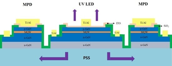
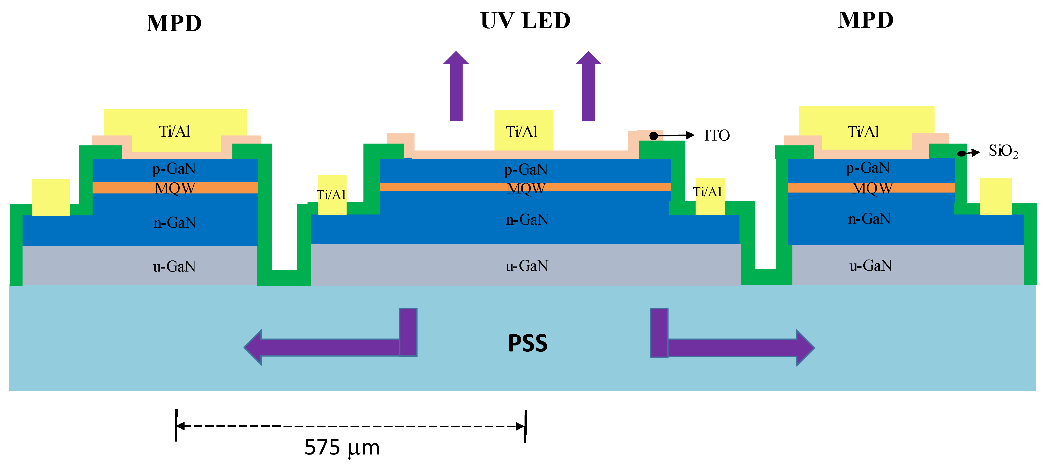
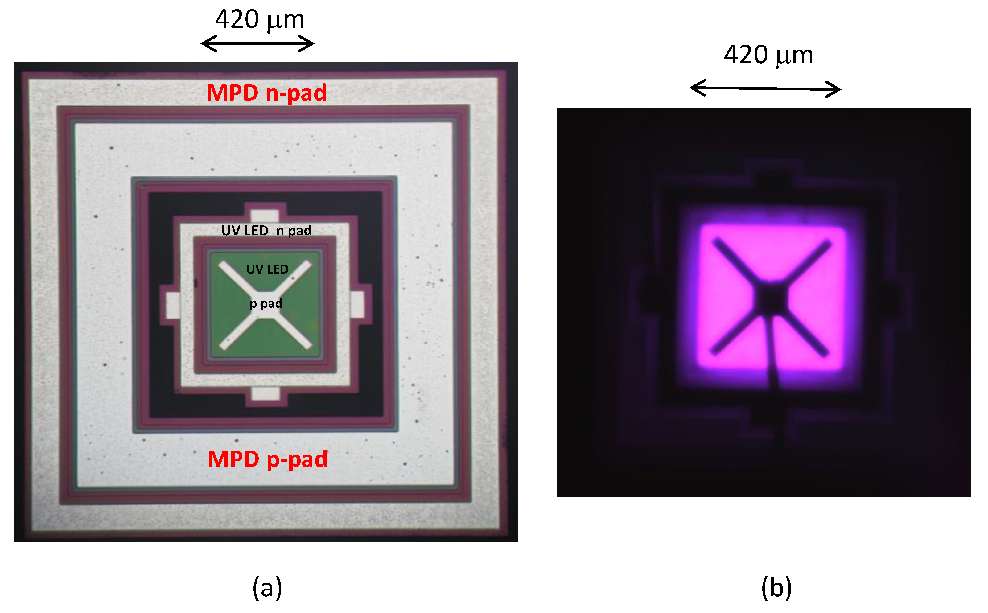
2. Device Structure and Fabrication

Figure 1 illustrates the monolithic UV LED and MPD. An LED epitaxial wafer commercially grown on a c-plane patterned sapphire substrate was used to fabricate the devices. Its emission spectrum exhibited a peak wavelength and full-width-at-half-maximum of approximately 392 and 15 nm, respectively. The MPD was completely covered with p-contact metal on top to block any external incoming light and thus, detect internal incoming light only. The processing procedure is in the following. Each device was electrically isolated by a deep etch down to the insulating sapphire substrate through inductively coupled plasma reactive-ion etching (ICP-RIE). Next, ICP-RIE was used to produce mesas on the LED and MPD, which provided access to the n-GaN layer. Subsequently, a SiO2 insulation layer was deposited. Then, an electron beam evaporator was used to deposit a 200-nm-thick indium-tin oxide (ITO) layer, which was then, thermally annealed at 625 °C in ambient N2 for 8 min. Finally, p/n-contact electrodes were formed. After processing, the chip was p-side-up mounted on a non-transparent printed circuit board and wire-bonded.

3. Results

Figure 2 presents a top-view photo of the fabricated devices and the CCD image of the UV LED at 10 mA. The active area sizes of the UV LED and MPD were 0.20 and 1.20 mm2, respectively, and the center-to-center distance was 575 μm. In [12], a report was provided of the photocurrent as a function of the distance between a p–i–n photodiode and an integrated LED with the same size; the responsivity was approximately 0.12 mA/W at a distance of 1 mm. Herein, we designed devices with a smaller center-to-center distance and larger MPD-to-LED size ratio to improve MPD responsivity.

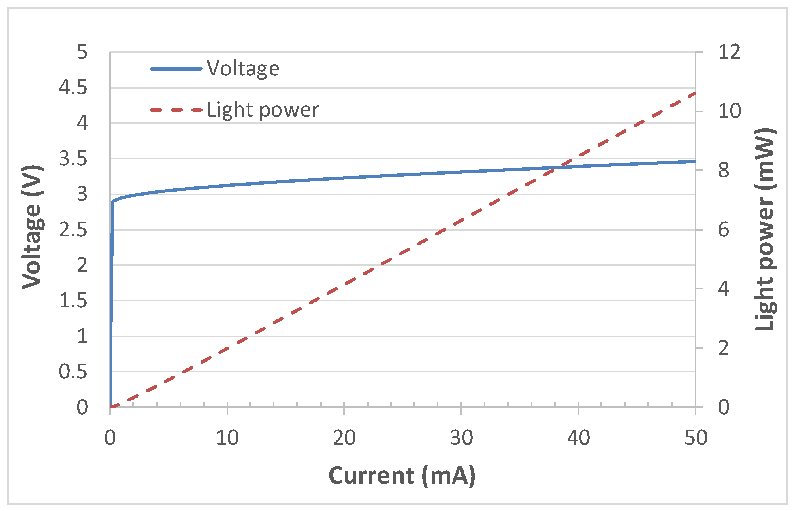
3.1. Basic Characterization

Figure 3 presents the voltage–current–light power (V–I–L) characteristics of the UV LED. The turn-on voltage and series resistance were approximately 3.0 V and 10 Ω, respectively. Figure 4 shows the emission spectrum (in a dashed line) of the UV LED when forward biased. On the other hand, because the MPD was protected from external incoming light, we used a reverse-biased LED acting as a p–i–n photodiode to evaluate our photodiode’s external quantum efficiencies (EQE) as a function of incident light wavelength at various photodiode biases at room temperature. The EQE measurement was conducted by using an incident photon-to-electron conversion efficiency system employing a broadband 300-W xenon lamp (Newport, model #6258), monochromator (Newport, model #74024), and lock-in amplifier (Newport, SR830). The peak EQEs were 50%, 55%, 61%, and 66% at 0, 1.5, 3, and 5 V, respectively. The results are plotted on Figure 4 with solid lines. These EQE values were typical for a p–i–n photodiode and corresponded to peak responsivities of approximately 0.16, 0.17, 0.19, and 0.21 A/W at 0, 1.5, 3, and 5 V, respectively, if the incident light was of wavelengths of peak EQE values and of normal incidence to the photodiode. However, for a same-chip MPD sharing the same bandgap material as the light source (UV LED), the incident wavelengths (392 ± 8 nm) were near the cut-off wavelength (approximately 405 nm). Additionally, the incident light (of the MPD) was only partially coupled from the UV LED emission, partially propagated through the sapphire substrate, and was incident on the MPD at various angles. Therefore, the monitoring responsivity was considerably lower than the peak responsivity.

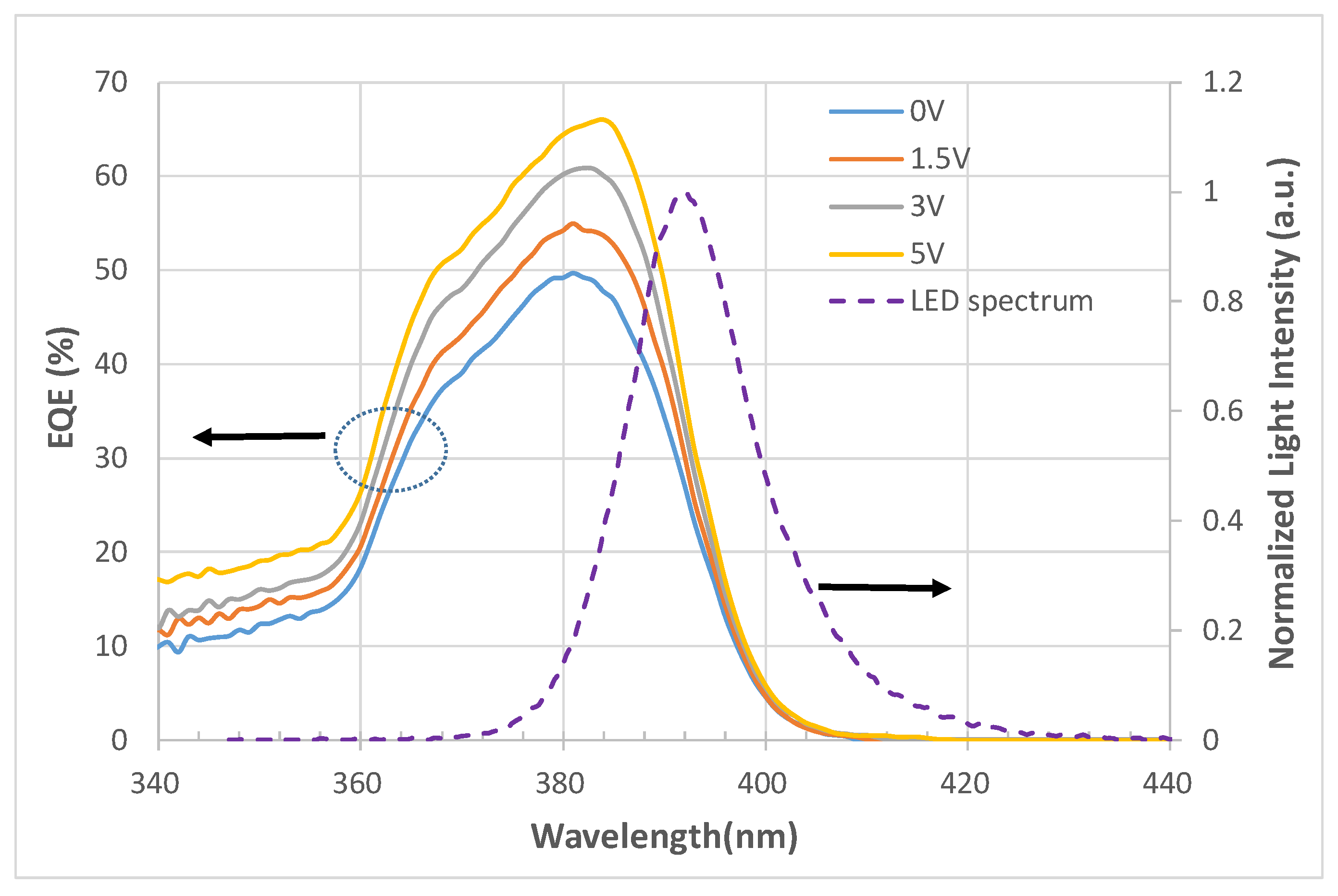
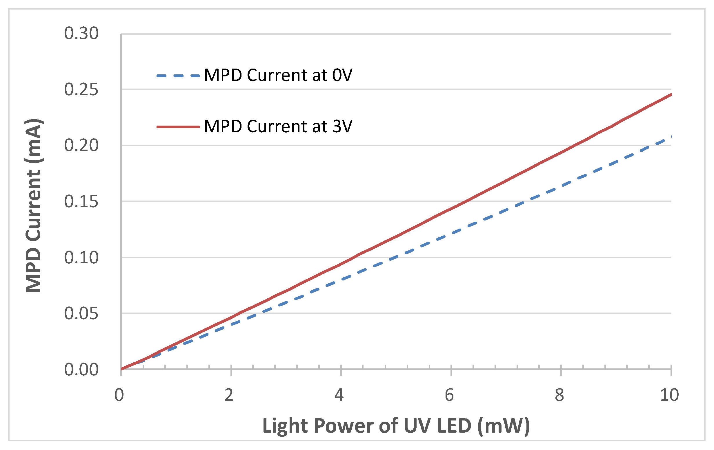
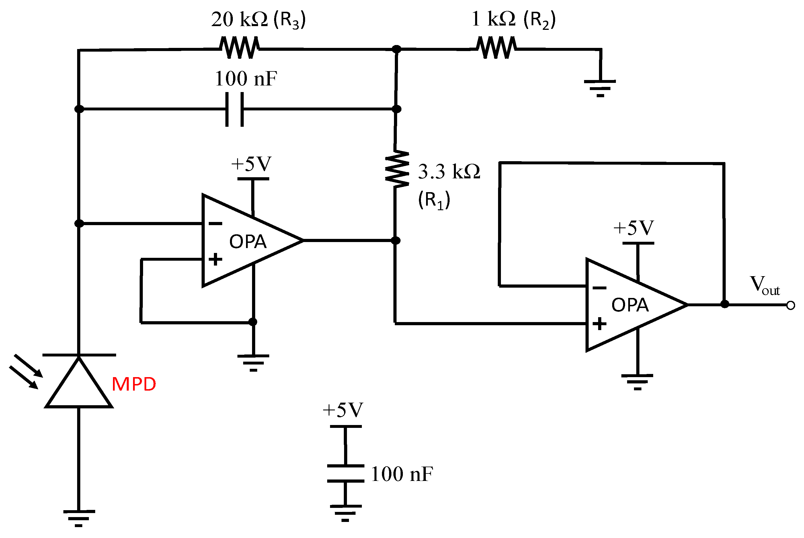
3.2. Monitoring Responsivity

Figure 5 presents the MPD currents obtained at 0 and 3 V biases with dark currents of approximately 0.22 and 3.5 nA, respectively, as a function of the surface-emitting power of the UV LED at room temperature. The curves were very linear, corresponding to monitoring responsivities of approximately 21 and 25 mA/W at 0 and 3 V biases, respectively. When combined with a transimpedance amplifier, i.e., a current to voltage converter having a transimpedance gain of approximately 8.9 × 10⁴ V/A, and a voltage follower (Figure 6), the resulting monitoring responsivity was approximately 1.87 V/mW at zero bias for the MPD. Based on the operating optical power range of the UV LED and the desired output voltage range of the MPD, an appropriate monitoring responsivity in a unit of V/W can be obtained by adjusting the gain of the transimpedance amplifier. From Kirchhoff’s rules, the output voltage Vout in Figure 6 followed Equation (1):
Vout = I [(1 + R3/R2)R1 + R3]
where I was the MPD current.

4. Discussion

The UV LED herein was located at, but not restricted to, the central region. The total power of UV LEDs can be scaled up by adding more LEDs adjacent to the MPD, though the resulting responsivity would be different. The shape of the MPD is not limited to being a loop, and could be a cross or a star that collects scattered light from LEDs. At the same time, the MPD might serve as a buffer between heat-generating LEDs to assist heat dissipation.
Secondly, sapphire has a large bandgap of approximately 9 eV [14] that is transparent to any emission wavelengths from AlGaInN-based LEDs, including UV LEDs from 200 to 390 nm in wavelength. The LED wafer used in this work emitted UV-A light; for UV-B or UV-C (e.g., 275 nm) LEDs, the cladding materials would become AlN and/or high-aluminum-ratio AlxGa1-xN, which are transparent to the emission wavelength of the active region; therefore, emitted light can be coupled partially to the sapphire substrate, and on-chip power monitoring via sapphire substrate still applies. For AlGaInN grown on Si substrate, fabrications of UV photodiodes or UV LEDs were reported [15,16,17]. However, it is unlikely to monitor UV power via Si substrate, because silicon itself highly absorbs UV light. As long as AlGaInN-based LEDs are grown on a sapphire substrate, no matter what orientations (polar, nonpolar, or semipolar [18]), on-chip power monitoring via sapphire substrate would be feasible.

5. Conclusions

On-chip power monitoring of a UV-A LED via sapphire substrate is reported. The UV LED was surrounded by a p–i–n photodiode loop with a center-to-center distance of 575 μm and an MPD-to-LED size ratio of six. Scattered light propagating through the sapphire substrate generated a photocurrent linearly proportional to the surface-emitting power. Monitoring responsivities of approximately 21 and 25 mA/W at MPD biases of 0 and 3 V, respectively, were obtained. When combined with a transimpedance amplifier, a monitoring responsivity of 1.87 V/mW at zero MPD bias was obtained. A different monitoring responsivity can be customized by adjusting the gain of the transimpedance amplifier.

Author Contributions

Conceptualization, P.S.Y.; investigation, C.-H.C., J.-J.Z., C.-H.W., T.-C.C. and R.-X.C.; writing—original draft preparation, C.-H.C., J.-J.Z. and C.-H.W.; writing—review and editing, P.S.Y. All authors have read and agreed to the published version of the manuscript.

Funding

This research was funded by Ministry of Science and Technology of Taiwan (MOST), grant number 108-2221-E-011-076 and 108-2218-E-011-009.

Conflicts of Interest

The authors declare no conflict of interest.

References

  1. Tchernycheva, M.; Messanvi, A.; Bugallo, A.L.; Jacopin, G.; Lavenus, P.; Rigutti, L.; Zhang, H.; Halioua, Y.; Julien, F.H.; Eymery, J.; et al. Integrated photonic platform based on InGaN/GaN nanowire emitters and detectors. Nano Lett. 2014, 14, 3515–3520. [Google Scholar]
  2. Jiang, Z.; Atalla, M.R.M.; You, G.; Wang, L.; Li, X.; Liu, J.; Elahi, A.M.; Wei, L.; Xu, J. Monolithic integration of nitride light emitting diodes and photodetectors for bi-directional optical communication. Opt. Lett. 2014, 39, 5657–5660. [Google Scholar]
  3. Li, K.H.; Cheung, Y.F.; Cheung, W.S.; Choi, H.W. Confocal microscopic analysis of optical crosstalk in GaN micro-pixel light-emitting diodes. Appl. Phys. Lett. 2015, 107, 171103. [Google Scholar]
  4. Li, K.H.; Cheung, Y.F.; Tang, C.W.; Zhao, C.; Lau, K.M.; Choi, H.W. Optical crosstalk analysis of micro-pixelated GaN-based light-emitting diodes on sapphire and Si substrates. Phys. Status Solidi A 2016, 213, 1193–1198. [Google Scholar]
  5. Li, K.H.; Fu, W.Y.; Cheung, Y.F.; Wong, K.K.Y.; Wang, Y.; Lau, K.M.; Choi, H.W. Monolithically integrated InGaN/GaN light-emitting diodes, photodetectors, and waveguides on Si substrate. Optica 2018, 5, 564–569. [Google Scholar]
  6. Li, K.H.; Cheung, Y.F.; Fu, W.Y.; Wong, K.K.Y.; Choi, H.W. Monolithic integration of GaN-on-sapphire light-emitting diodes, photodetectors, and waveguides. IEEE J. Sel. Top. Quantum Electron. 2018, 24, 3801706. [Google Scholar]
  7. Wang, Y.; Zhu, G.; Cai, W.; Gao, X.; Yang, Y.; Yuan, J.; Shi, Z.; Zhu, H. On-chip photonic system using suspended p-n junction InGaN/GaN multiple quantum wells device and multiple waveguides. Appl. Phys. Lett. 2016, 108, 162102. [Google Scholar]
  8. Shi, Z.; Gao, X.; Yuan, J.; Zhang, S.; Jiang, Y.; Zhang, F.; Jiang, Y.; Zhu, H.; Wang, Y. Transferrable monolithic III-nitride photonic circuit for multifunctional optoelectronics. Appl. Phys. Lett. 2017, 111, 241104. [Google Scholar]
  9. Wang, Y.; Wang, S.; Ni, S.; Wang, W.; Shi, Z.; Yuan, J.; Zhu, H. On-chip multicomponent system made with vertical structure quantum well diode. Semicond. Sci. Technol. 2019, 34, 065017. [Google Scholar]
  10. Liu, C.; Cai, Y.; Jiang, H.; Lau, K.M. Monolithic integration of III-nitride voltage controlled light emitters with dual-wavelength photodiodes by selective-area epitaxy. Opt. Lett. 2018, 43, 3401–3404. [Google Scholar]
  11. Yeh, P.S.; Chiu, Y.-C.; Wu, T.-C.; Chen, Y.-X.; Wang, T.-H.; Chou, T.-C. Monolithic integration of GaN-based phototransistors and light-emitting diodes. Opt. Express 2019, 27, 29854–29862. [Google Scholar]
  12. Chiu, Y.-C.; Yeh, P.S.; Wang, T.-H.; Chou, T.-C.; Wu, C.-Y.; Zhang, J.-J. An ultraviolet sensor and indicator module based on p–i–n photodiodes. Sensors 2019, 19, 4938. [Google Scholar]
  13. Feng, M.; Wang, J.; Zhou, R.; Sun, Q.; Gao, H.; Zhou, Y.; Liu, J.; Huang, Y.; Zhang, S.; Ikeda, M.; et al. On-chip integration of GaN-based laser, modulator, and photodetector grown on Si. IEEE J. Sel. Top. Quantum Electron. 2018, 24, 8200305. [Google Scholar]
  14. French, R.H. Electronic band structure of Al2O3, with comparison to Alon and AIN. J. Am. Ceram. Soc. 1990, 73, 477–489. [Google Scholar]
  15. Yusoff, M.Z.M.; Hassan, Z.; Hassan, H.A.; Abdullah, M.J.; Rusop, M.; Pakhuruddinb, M.Z. AlxGa1–xN/GaN/AlN heterostructures grown on Si(1 1 1) substrates by MBE for MSM UV photodetector applications. Mater. Sci. Semicond. Process. 2015, 34, 214–223. [Google Scholar]
  16. Li, Y.; Wang, W.; Huang, L.; Zheng, Y.; Li, X.; Tang, X.; Xie, W.; Chen, X.; Li, G. High-performance vertical GaN-based near-ultraviolet light-emitting diodes on Si substrates. J. Mater. Chem. C 2018, 6, 11255. [Google Scholar]
  17. Aiello, A.; Wu, Y.; Mi, Z.; Bhattacharya, P. Deep ultraviolet monolayer GaN/AlN disk-in nanowire array photodiode on silicon. Appl. Phys. Lett. 2020, 116, 061104. [Google Scholar]
  18. Fan, X.; Xu, S.; Li, P.; Zhang, J.; Peng, R.; Zhao, Y.; Du, J.; Hao, Y. Nonpolar and semipolar ultraviolet multiple quantum wells on GaN/sapphire. Mater. Sci. Semicond. Process. 2019, 92, 103–107. [Google Scholar]
Figure 1. Schematic structure of the monolithic UV LED and MPD, where ITO and PSS represent indium-tin oxide and patterned sapphire substrate, respectively.
Photonics 07 00063 g001
Figure 2. (a) A top-view photo of the fabricated UV LED and MPD; (b) an image of the UV LED at 10 mA in the dark.
Photonics 07 00063 g002
Figure 3. V–I–L characteristics of the UV LED.
Photonics 07 00063 g003
Figure 4. EQE versus wavelength at various biases at room temperature when measured as a p–i–n photodiode (in solid lines), and the emission spectrum when measured as an LED (in a dashed line).
Photonics 07 00063 g004
Figure 5. MPD current versus light power of the UV LED.
Photonics 07 00063 g005
Figure 6. Schematic diagram of the MPD at zero bias, a transimpedance amplifier, and a voltage follower, where OPA represents an operational amplifier.
Photonics 07 00063 g006

