1. Introduction
Terahertz (THz) is a rapidly emerging field in science with many potential applications but where there is an urgent need for new ways of producing sources, detectors and other devices such as filters, sensors and modulators. Artificial materials, such as metamaterials, play an important role in THz because they make it possible to design and manufacture very compact, sensitive and extremely selective structures surpassing the existing materials in nature [
1,
2]. Over the last few years, the scientific community has focused on several research areas, such as all-dielectric metamaterials, reconfigurable metamaterials, flexible metamaterials, metadevices, graphene metamaterials, tunable metamaterials and metasurfaces [
1,
3]. According to [
2], for sensing applications, it is necessary that metamaterials are capable of fulfilling a set of requirements such as the ability to provide spoof surface plasmons with localized electric field enhancement and have high quality factor values (
Q-factor), while preserving a high sensitivity, even when subjected to minor changes due to external factors. Some classes of metamaterials have gained a significant prominence for this type of applications, namely metasurfaces, absorbers, metallic mesh devices and metamaterial-based thin films, due to their potentialities in terms of shape design, geometry, orientation, maximization of the excited electric/magnetic field, tuneability, sensitivity and also the possibility of being manufactured using lithography and nanoprinting technologies [
1,
3]. Successful applications have been reported in the literature with an emphasis on biosensing, microfluid devices, THz detectors and plasmonic toroidal metamodulators [
2,
3,
4,
5]. Architectonically speaking, most of these devices are based on split ring resonators (SRRs) and frequency-selective surfaces (FSSs), whose geometric and quality parameters can be adjusted to efficiently control resonant modes, quality factor, sensitivity, selectivity, responsivity and also to minimize losses. However, new trends in this field report a paradigm change in which the inclusion of nanomaterials in metamaterial sensors and the use of graphene plasmon and graphene metamaterial devices and topological insulators induced THz surface are expected in the near future [
1].
THz filters are a key component in optimizing the performance of THz sensing devices, since they can eliminate undesirable background radiation and enhance the signal-to-noise ratio as well as spectral resolution in practical applications such as THz spectroscopy and imaging [
6,
7]. Several designs of broadband and narrowband THz bandpass filters based on metamaterials have been studied over the last decade [
8,
9,
10,
11,
12]. Narrowband THz filters are especially important since they are the centerpiece of a wide range of ultrasensitive THz sensors due to their capability for selecting the radiation only in a narrow spectrum around a target frequency [
10]. There is a wide range field where those sensors are essential, such as health, industry, science, telecommunications and security [
6,
7,
10]. Several approaches related to the design of THz filters as well as to their tunability, have been reported since then. Some examples that stand out include the architectures based on photonic crystals, thin-film stacks, Bragg reflectors, FSSs, waveguides and resonant cavities [
13,
14,
15,
16,
17]. The performance of most of these filters can be controlled following the same methodologies used in metamaterials, being also possible to control them mechanically (by adjusting the thickness or the distance of the components of the unit cells) or through the action of temperature as described in [
6,
15]. Metrics such as dynamic range,
Q-factor, full width at average maximum (FWHM), dephasing time of the induced spectral line shapes (
), figure of merit (
) and insertion loss (IL) are widely used to evaluate THz filters [
5,
6,
13,
14,
17].
The utilization of THz technologies for stress sensing applications is very recent, but some approaches have already been reported in the literature [
18,
19,
20,
21]. The sensors of those systems must be accessible, light and discrete, so as not to impose cost and weight on the structure as well as not to interfere with the structural resistance [
19]. Most of these requirements can be easily accomplished through the use of FSSs in the design of micro-electro-mechanical system (MEMS) sensors, since they can offer higher sensitivity and resolution and also possess a greater potential to deliver the strong enhancement and localization of fields, being especially suitable for the development of wireless strain sensors that can operate in the microwave and terahertz ranges [
18,
21]. The development of THz stress sensors based on metal mesh filters and FSSs is described in [
21]. The resonances of this type of sensor are obtained thanks to the periodicity of the unit cells in the direction of propagation and, according to the authors, can be used in several applications, including structural health monitoring (SHM). Their integration into the structures allow us to detect cracks and other kinds of damage, since, in this type of critical situation, it is known that the reflectance/transmittance values of the sensors decrease abruptly.
This paper aims to present a detailed study about the characterization, design and simulation of a reconfigurable THz filter with high sensitivity and selectivity for sensor devices such as stress sensors. Our filter has a simpler design when compared to the approaches referred above, since it is composed by only two FSSs based on metamaterial wire resonators. Despite being a novel approach, the proposed device can provide a higher dynamic range, an enhanced frequency selectivity and requires less force to cause a frequency shift. The remainder of the paper is organized as follows:
Section 2 describes the filter theory and respective design. The mechanical model and respective simulation method is introduced in
Section 3, while
Section 4 presents the numerical results obtained from the electromagnetic and mechanical point of view. Finally, the conclusions are outlined in
Section 5.
2. Filter Theory and Design Decisions
In this section, the required tools are introduced in order to design a highly selective structure (HSS) that is the centerpiece of the sensor. This HSS works as a reconfigurable selective THz window in which only radiation of certain desired frequencies is allowed to pass. In literature, as described in [
21], this kind of behavior is obtained using a technique related to the periodicity of the unit cells of the structure in the direction of propagation. Here, a much simpler approach, where the resonances are obtained from the propagation in a THz HSS composed by two arrays of gold wires, is used. The goal is therefore to study the interaction between the waves and the wires to be able to understand the principle of operation of the HSS. More specifically we intend to devise a method to optimize the relation between the radius of the wires and the distance between wires and adjust the sensitivity and selectivity of the device. Moreover, for simplicity, we shall assume that the structure is composed by two arrays of wires because using a single array would not be sufficient to achieve the desired degree of selectivity. Based on the variation of the distance between wires and the mechanical stress experienced by the structure, it will be possible to predict how the transmittance is decreasing to the operating frequency, since, when the transmittance is very low when compared to the initial one, it is known that the structure has a problem.
2.1. Working Principle
In this paper, we propose a new design for a reconfigurable THz filter that can be used to implement an electro-mechanical sensor. As can be seen in
Figure 1, the device is composed of two FSSs (arrays of wires) within a dielectric host material. Note that the selective character of the wire arrays gives rise to a bell-shaped frequency response. The working principle is presented in
Figure 1, in which it can be seen that by applying compression along the
axis, the distance between wires
will decrease and, therefore, the frequency response of the sensor will change, as does its transmittance. The sensor is settled to operate at the target frequency and, as it experiences compression, it becomes possible to adjust the sensor response from full transparency to complete opacity, including all degrees of transparency in between. The red curve corresponds to maximum compression and the green curve to half compression.
By allowing a lateral compression instead of a uniaxial compression, the device becomes more functional and easier to implement. It is also more selective since its working principle is based on the resonance of two arrays in the propagation directions. This selectivity can be accomplished through the careful design of the ratio of the wire arrays ( is the radius of the wires), which also enhances the -factor of the filter.
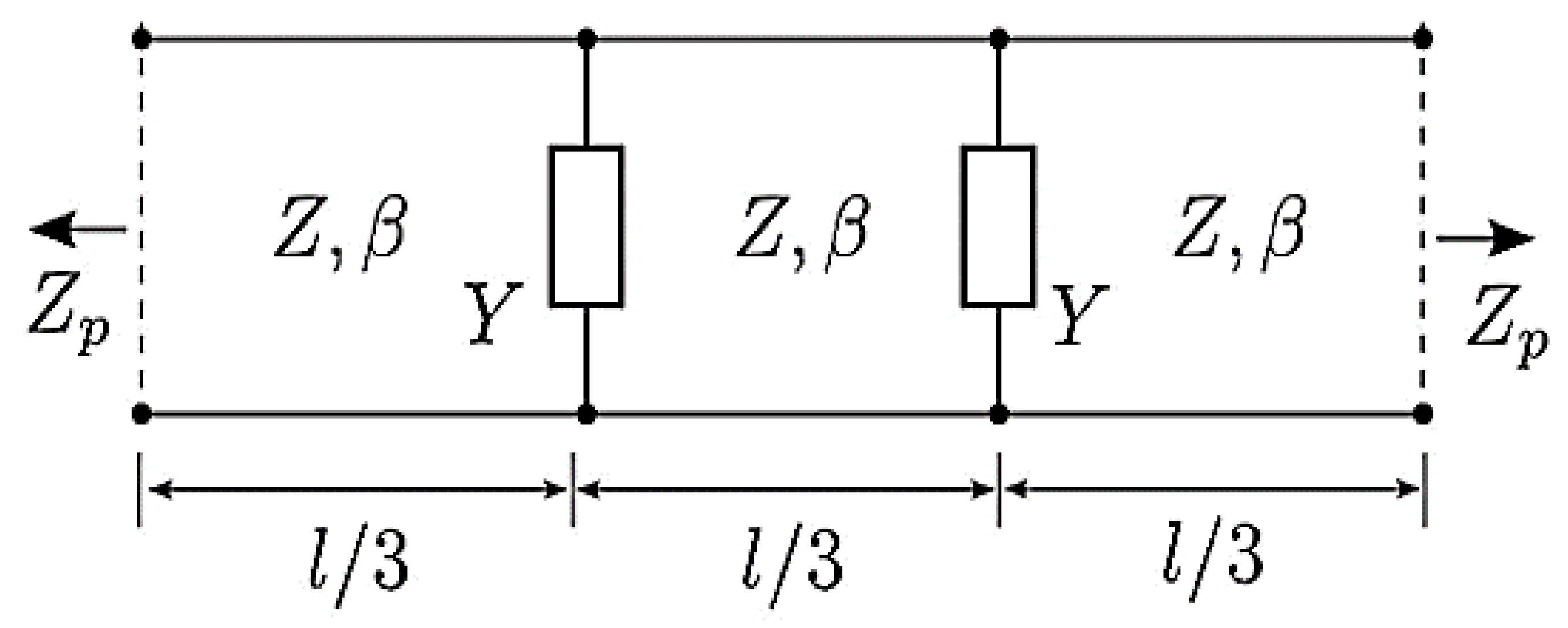
This double grid structure can be represented by a simplified two-port network model, as can be seen
Figure 2 [
22]. The arrays of wires are described as admittances
in the equivalent circuit and the dielectric slab is represented by three sections of transmission line with equal length
(note that the total length of the structure is
).
In this model, is the impedance of the port, is the characteristic impedance of the dielectric slab material and β is the propagation constant. In the next section, we will show how to determine the expression for admittance .
2.2. Circuit Theory
In all wave propagation problems, where there are transitions between media, we can always identify incident waves at the interface, which give rise to reflected and transmitted waves. As it is well known from electromagnetic theory, the reflectance and transmittance of a dielectric slab have a comb like frequency response [
22]. However, in this situation, the arrays of wires will introduce a filter-like response in the frequency domain. We must study this problem in order to understand the interactions between electromagnetic waves and the array of wires, as can be seen in
Figure 3. By studying the problem, we will be able to find out what will be the structure’s response in the frequency domain and how can we tune the filter.
2.2.1. Equivalent Circuit Admittance for the Wire Arrays
For propagation in the
direction and for time harmonic fields of the form
, the Helmholtz equation is:
where
is the magnitude of the wave vector and
is the
component of the electric field, parallel to the wires. Solutions of (1) can be written in the form
, where
The second term on the right-hand side vanishes because
. This condition results from the symmetry along the
y axis. Moreover, since the structure is periodic in the
direction with lattice constant
, the possible solutions for
, in the Fourier plane are restricted to
, where
is the number of the propagation mode. The condition in this case is
. Thus, we can write:
For the
component of the wavevector, we have
, where
This follows from
if we take into account that
, which corresponds to the case where it is not possible to resolve details in the structure according to Abbe limit. The solutions for
are of the form
and
, which describe evanescent waves that only exist in the vicinity of the wires. The electric field for
is then given by:
where
and
are the complex amplitudes of the incident and reflected waves, respectively, and the coefficients
account for the evanescent fields. For
the electric field is obtained by combining the transmitted wave with the evanescent field:
Close to the wires we have
, where
and
At the wires (
), the tangential component of the electric field must be continuous. We have:
which, according to Fourier’s theory implies that:
For cylindrical wires, it is convenient to introduce the following function:
which has the geometric property of being approximately constant on the surface of the thin wires. By Taylor expansion we find:
where the
sign holds for
and the
sign for
. Based on this expansion, we can assume
and write the electric field
in terms of
as
To determine
in terms of
, we impose the continuity of
at
. With the aid of the Equations (10) and (13), we find:
Up to this point, we have neglected the boundary conditions on the surface of the wires, where the tangential component of the electric field
must vanish. Considering wires with radius
, it results from (14) and using (13) with
and
that:
where we have also used (11) to determine
. From network theory [
22], we known that the
parameters of a two port circuit consisting of an admittance
are
,
and
, such that:
Here,
is the characteristic impedance of the dielectric slab material. Hence, (16) is compatible with (15) and we can easily determine the admittance.
2.2.2. Transmission Matrix of the Filter
Let
and
be the transmission matrices of a section of the slab of size
and of a two-port network consisting of an admittance
, respectively. Then, the
parameters for the equivalent circuit in
Figure 2 can be written in the form:
where
,
and
are the following normalized impedances:
with coefficients
and
defined as:
and
Knowing the
parameters of the network, one can determine the scattering matrix using the formulas for the conversion between two-port network parameters [
22]:
and
where
is the normalized impedance of the slab with respect to free-space. By symmetry and reciprocity, we have
and
.
2.3. Parameters’ Choice
The theory described above was used to determine a starting point for the device parameters assuming a frequency window in the THz range between 395 and 455 GHz. From the theoretical model, it is possible to verify that the bandwidth decreases as increases. Moreover, as we approach the limit , the will grows to . However, this value cannot be reached due to the resistance of the wires and because in that limit the formula is only an approximation (formula is only valid for and ). After performing several electromagnetic simulations to fit tune the initials parameters, a set that fulfill our requirements was found:
The distance between wires is expressed as a range, since the previous study proved that it is possible to control the behavior of the filter in the desired frequency range by varying this parameter and to compress the device without deforming or cracking the structure [
21]. As mentioned above, the device must have some robustness and a good degree of sensitivity, which means that one should consider materials that will be relatively easy to compress and transparent to THz radiation. According to [
18], silicon and plastics such as high-density polyethylene (HDPE) and polytetrafluoroethylene (PTFE) are key terahertz materials since they fulfil the requirements mentioned above for the frequency band over 0.1 to 5 THz [
23]. Naturally, the plastic materials will be a more suitable solution since silicon requires a substantially higher rate of compression. However, it is also important to consider some specific characteristics from the materials, taking into account the working principle, the design and the assembly of the filter.
HDPE possesses a linear structure with few branches lending to its optimal strength/density ratio. This thermoplastic presents some interesting features, such as: the sensitivity to stress cracking and the possibility to customize their physical properties through the molding process that is used in its manufacturing [
24,
25]. On the other hand, PTFE, which is a material widely used in industrial applications, also presents some interesting features, such as: weatherability and the capability of maintaining high strength, toughness and self-lubrication at low temperatures down to 5 K, as well as good flexibility at temperatures above 194 K [
26].
Considering their properties and the fact that both have low losses and low dispersion in the frequency region of the THz, as mentioned above, these materials in fact constitute good candidates to be used in the assembly of the proposed device.
4. Results
In this section, the results from the simulations based on the design of the filter for each assembling hypothesis will be presented. Two analyses of the behavior from the electromagnetic and mechanical point of view will be carried out. By analyzing the data, we will also discuss how it will be possible to apply the desired compression level to the devices and thus control the distance between wires.
4.1. Return Loss and Insertion Loss in the Frequency Domain as a Function of Distance between Wires
After the conception and presentation of the theoretical study of the working principle of the filter, it is necessary to corroborate the accuracy of the conceived theoretical model through simulations, as well as to analyse some relevant issues such as: the dynamic range, the periodicity of the shifts of resonance frequency and the evolution of the bandwidth of the device under compression.
Knowing that HDPE and PTFE have different relative permittivity constants, it will be necessary to analyse the filter for both assembling cases. Note that HDPE has a relative dielectric constant
εr = 2.4 and PTFE posseses
εr = 2.1 [
26]. The losses were not considered due to the characteristics of these materials, as highlighted in
Section 2.
The resonance frequency () will be shifted to higher frequencies as the filter is compressed. The reduction in the distance between wires occurs with a step size of 0.5 μm.
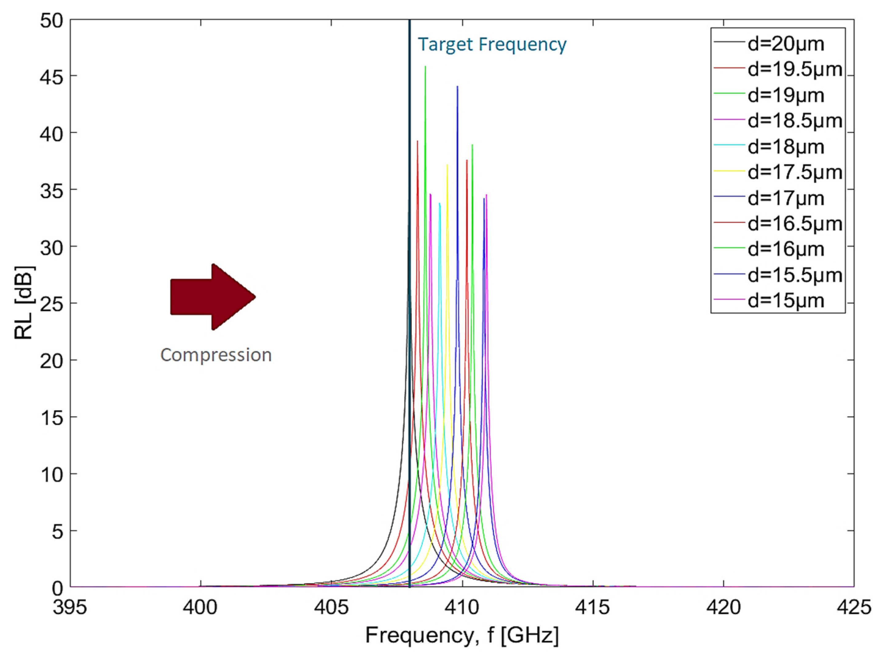
4.1.1. HDPE
Figure 5 and
Figure 6 shows return losses (RL) and insertion losses (IL) in the frequency domain as a function of applied compression for the HDPE host medium. These quantities were calculated based on the results obtained for the scattering parameters from the simulations. Since the structure is invariant to port swapping in the propagation direction, we might consider the following formulas
and
, respectively [
22]. The device resonance, without compression, is at 408 GHz, but, when we imposed a full compression (25%), the resonance changes to 411 GHz. In every curve, each reduction of 0.5 µm in the distance between wires causes an increase of 278 MHz in the resonance frequency, which is followed by an average bandwidth reduction at 3 dB of 111 MHz. Considering this data, it is possible to state that, between these two extreme cases, there was a shift of 3 GHz in resonant frequency and a reduction in the bandwidth at 3 dB of 1.1 GHz (a decrease of more than 50% when compared with the initial value without compression). Some saturation and distortion in the filter response are expected for this reason.
In
Figure 5 and
Figure 6, there is a vertical line identifying the target frequency (408 GHz) and, by analyzing both of them, it can be seen that the device presents an excellent dynamic range along this curve. This means that, as compression is applied to the device, it will go from full transparency (
= 0) to full opacity (
= 1). Therefore, it is possible to conclude that the bandwidth decreases and the selectivity increases as the compression is applied to the filter.
The FWHM decreases from 1.2 GHz (without compression) to 0.55 GHz (maximum compression) [
5]. The quality factor can be calculated as the ratio between the resonance frequency and the FWHM. We found that the
Q factor ranges between
for the case without compression and
when maximum compression is applied. Considering the same criteria that was used to analyze the previous metrics, we found that the dephasing time
of induced line shapes decreases from 1.5797 to 0.724 µs [
5]. Moreover, the figure of merit can be defined as the number of passbands inside the range of tuning, which can be computed as:
where
is the uppermost resonant frequency,
is the lowermost resonant frequency,
is the uppermost passband width and
is the lowermost passband width, respectively [
6]. We estimated a
. The insertion losses (IL) are practically zero as the resonance frequency is shifted by the compression on the device. The high value of the return losses (RL) means that the reflected energy is very small when compared to the incident wave energy. These results show that the higher the compression level applied, the greater the selectivity of the device.
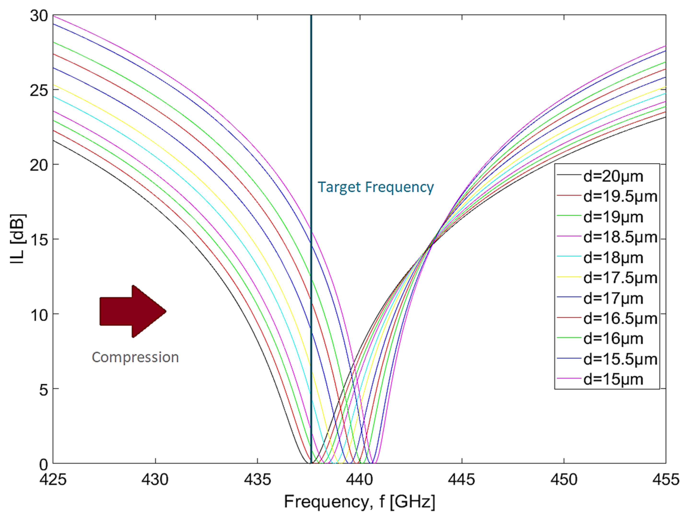
4.1.2. PTFE
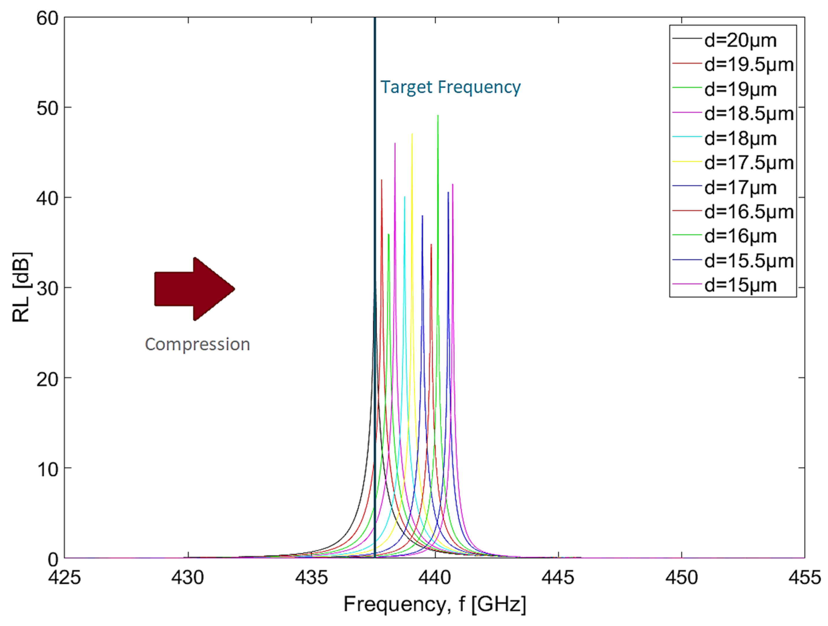
The results from the electromagnetic simulations for the filter assembled with PTFE are shown in
Figure 7 and
Figure 8. By observing both figures, it is possible to conclude that the behavior is slightly the same when compared to the case of HDPE. However, the resonances now occur at higher frequencies, since the parameters that characterize the material are different. Note that, without compression, the device presents a resonance at 437.5 GHz, which will change to 440.7 GHz when full compression is applied. In every curve, each reduction of 0.5 µm in the distance between wires causes an increase of 320 MHz in the resonance frequency, which is followed by an average bandwidth reduction at 3 dB of 122 MHz.
Considering these data, it is possible to state that the application of maximum compression caused a total shift of 3.2 GHz in the resonance frequency and a reduction in the bandwidth at 3 dB of 1.1 GHz (a decrease of 50% when compared with the initial value without compression). In
Figure 7 and
Figure 8, there is a vertical line identifying the target frequency (437.5 GHz) and, by analyzing both of them, it can be seen that the filter presents a slightly better dynamic range when compared to the case of the device assembled with HDPE. The FWHM decreased from 1.3 GHz (absence of compression) to 0.65 GHz (maximum compression), and, similar to what was observed previously, the progression of the resonance frequency as the filter is compressed is also approximately linear. The quality factor increased from
(absence of compression) to
(maximum compression) as the distance between wires is reduced. Considering the same criteria that was used to analyze the previous metrics, we found that the dephasing time decreases from
= 1.7114 µs to
= 0.8557 µs. Moreover, this filter presents an
, which was calculated by using Equation (25) and considering that
,
,
and
, respectively. Globally, these results are similar to what was obtained for the HDPE.
4.2. Reduction in the Distance between Wires as a Function of Required Current
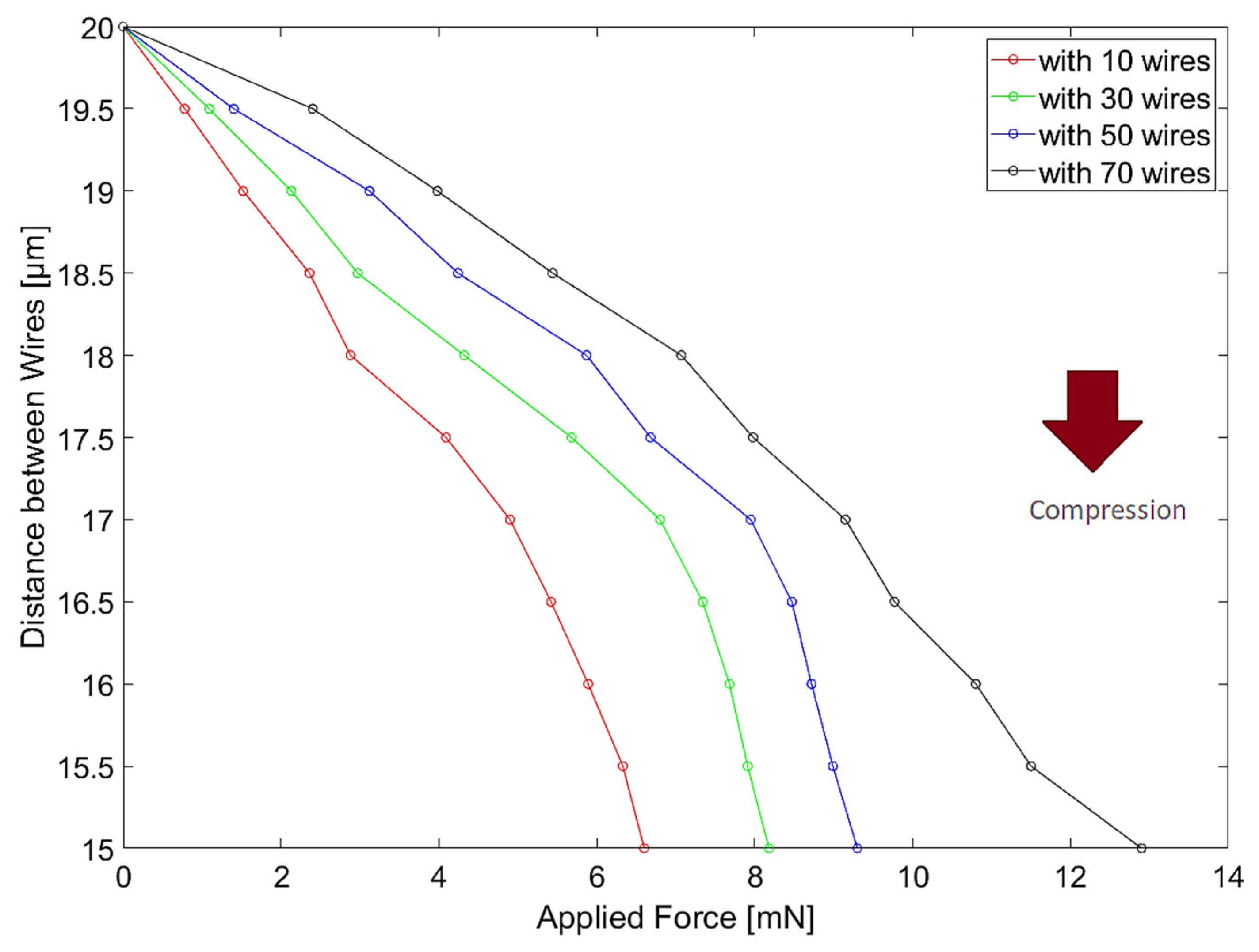
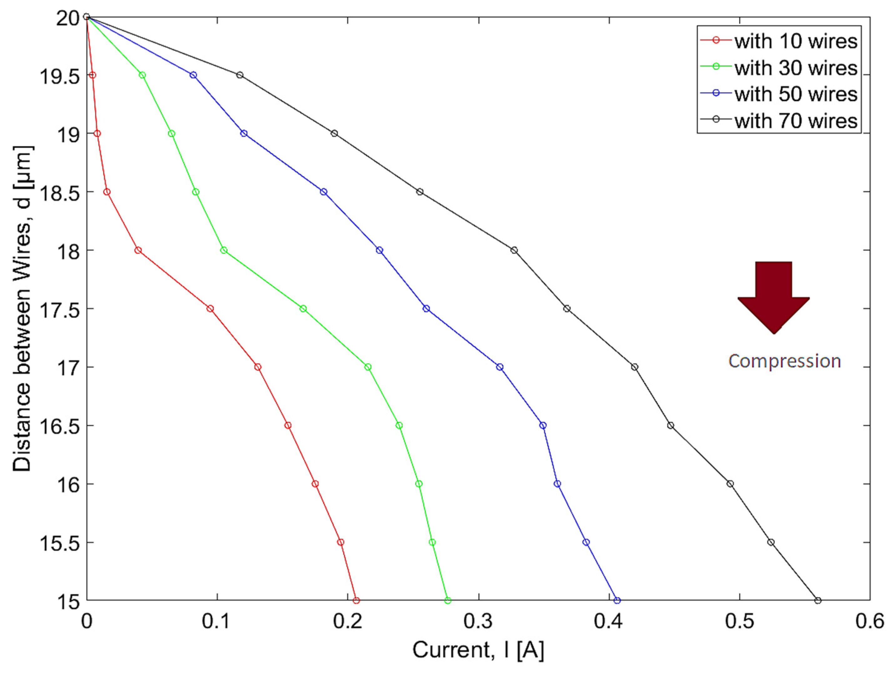
After performing the analysis of the electromagnetic component, we will focus on the analysis of the mechanical component. In the following subsections, we intend to understand how much force it will take to make the device compress up to 25% according to the materials used for its assembly and, knowing that there is a possibility of controlling the compression magnetically, what will be the current required to reach each level of compression. Through preliminary mechanical simulations, we found out that 70 wires per array are sufficient to obtain the desired behavior of the device. We also decided to study how the number of wires influences its response.
4.2.1. HDPE
Considering the theory associated with mechanical simulations, it is possible to predict the amount of force required to cause the desired distance between wires to be reduced in each case. By combining the theory used in the Elmer solver with the theory of magnetic circuits based on which the FEMM software solves the problems, we are able to discover the current required to cause the compression that allows the distance between wires to decrease.
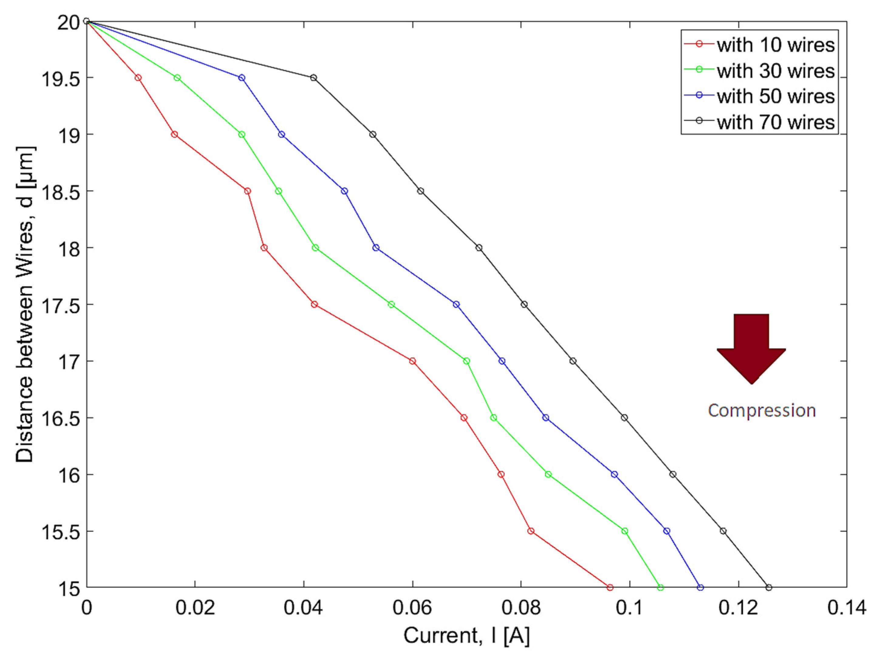
By analysing
Figure 9 and
Figure 10, it is observed that, as expected, the higher the force to be applied to the device, the higher the current to be supplied to the magnetic circuit. To fully compress the device with 70 wires, we should supply 0.56 A to the magnetic circuit.
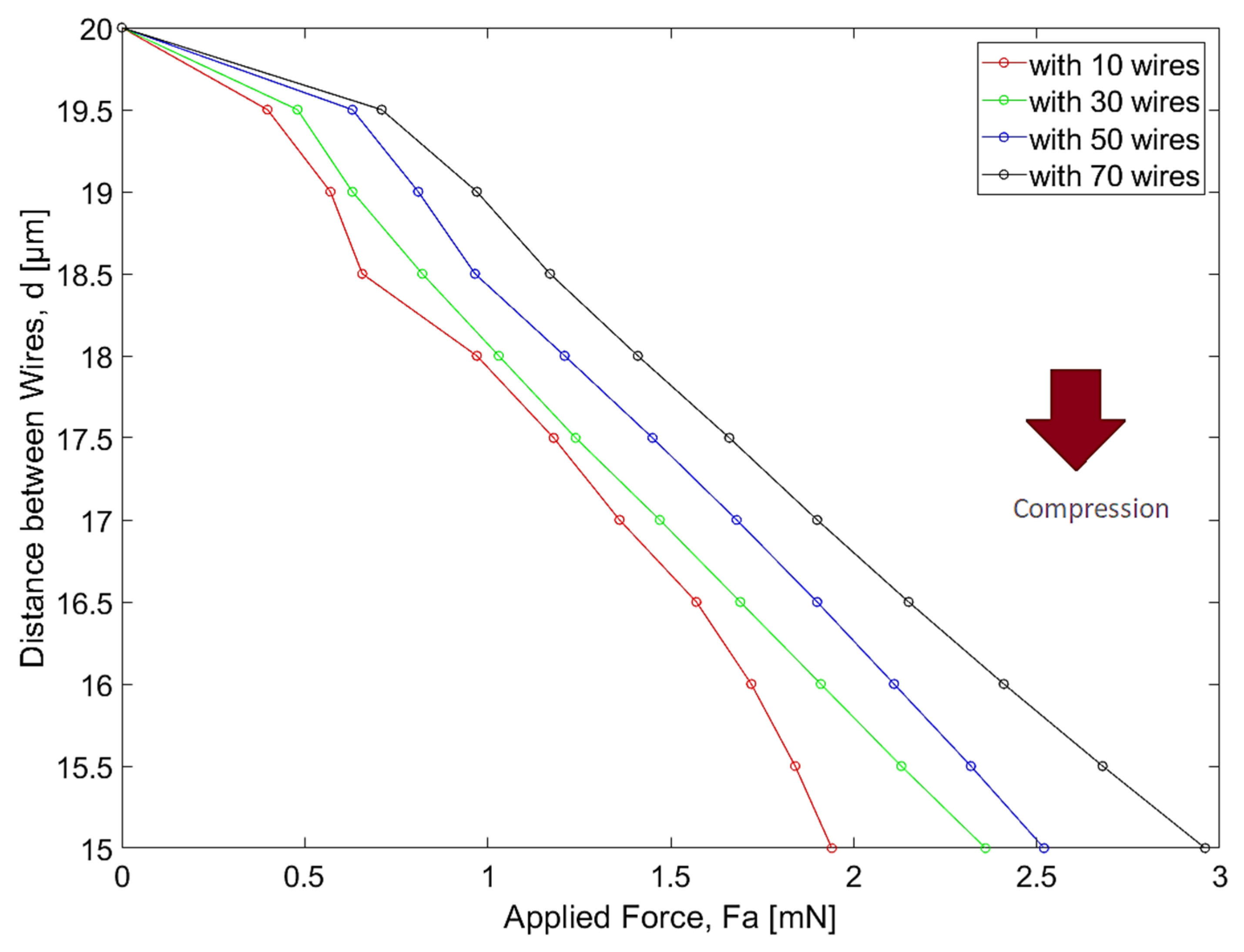
4.2.2. PTFE
Similar to the previous case, we obtained from the Elmer solver the range of forces to be applied to the filter in order to achieve each compression state. The results are presented in
Figure 11. After that, we obtained from the FEMM solver the range of currents to be supplied to the magnetic circuit in order to compress the device according to the previous data, as can be seen in
Figure 12.
The curves for the applied force and the required current have the same slope for each scenario, in which the number of wires is increased. However, in this case of PTFE, both the force and the current values are much lower. We should note that, as the range of forces to be applied for each typology is different, the range of currents to be supplied will also be different. In order to achieve a full compression of the device with 70 wires, we should supply the magnetic circuit with 0.125 A, which is substantially lower than the one required for HDPE.
4.3. Reflectance and Transmittance as a Function of Applied Force
Finally, after performing electromagnetic and mechanical simulations, we can now use the information we obtained from both components to illustrate the reflectance/trasmittance as a function of the force applied to the filter for each host material that can be used to build the device. The following graphs show us the relationship between these quantities. It should be noted that the resonance frequency was fixed taking into account the case without compression ( = 408 GHz and = 437.5 GHZ, respectively).
4.3.1. HDPE
Through a careful analysis of
Figure 13 and
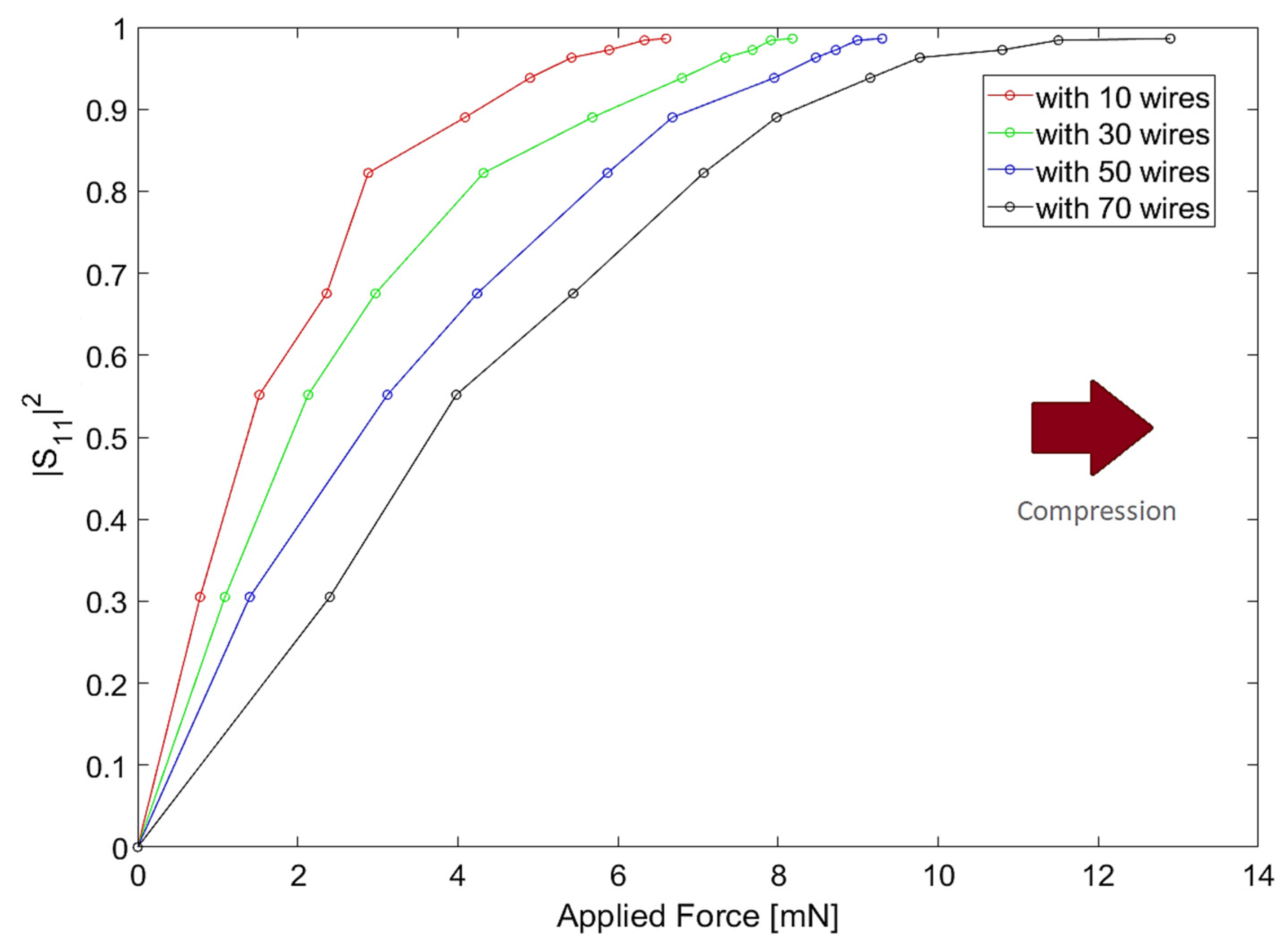
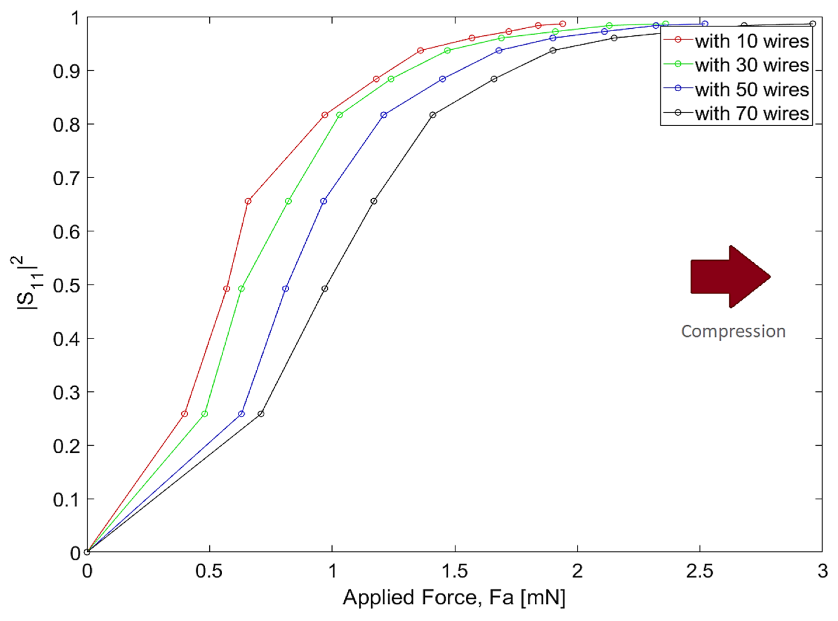
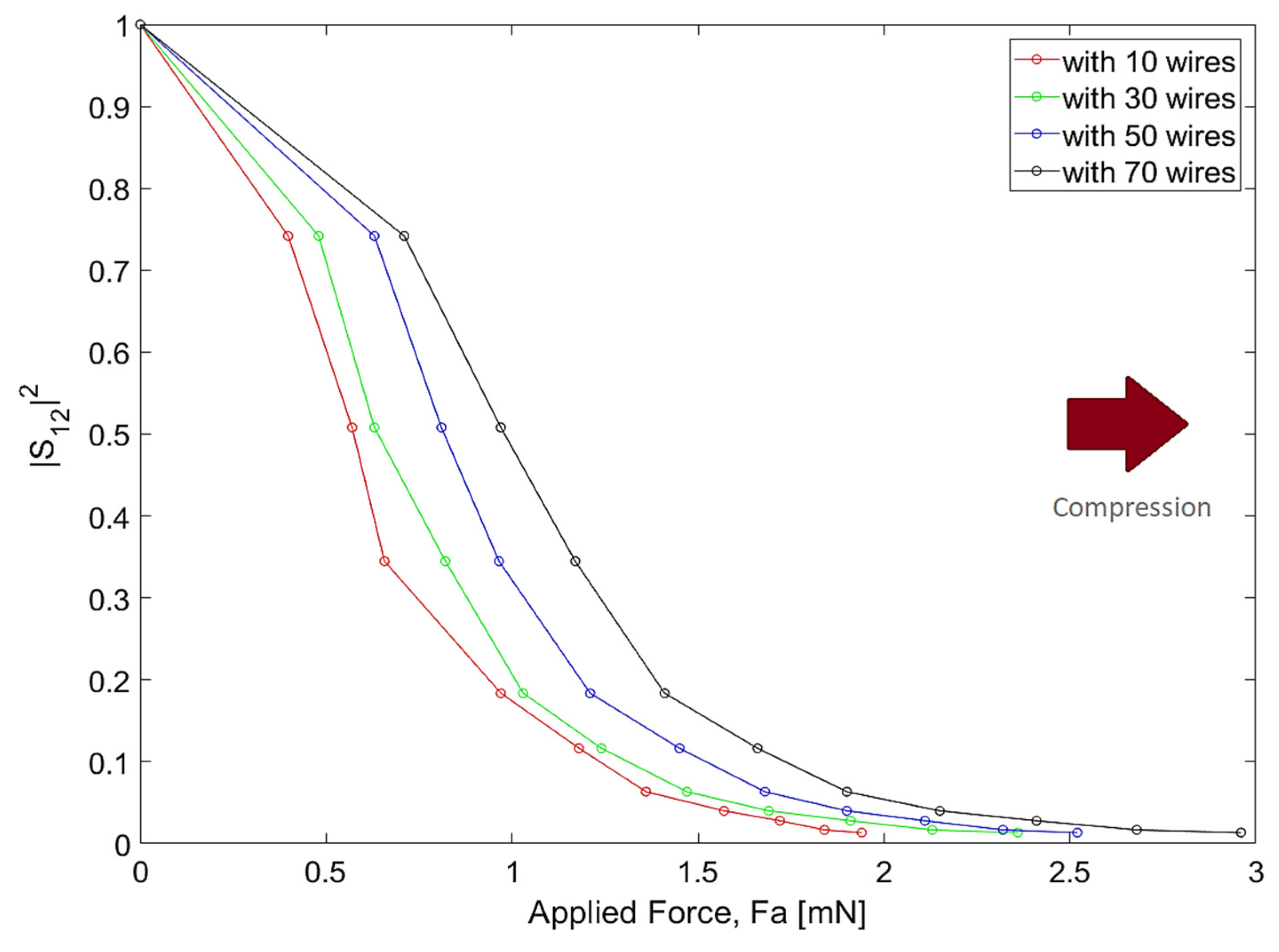
Figure 14, we observe that, by increasing the number of wires per array, the more linear the response of the filter will be. Independently of the curve under analysis, the device response presents some saturation for high values of applied force. If we focus on the designs with 50 or more wires, we observe saturation for values greater than 8 mN. In spite of this fact, the device can reflect almost all of the incident wave (more than 90%) and, therefore, we can assume that the device presents an approximately linear response in the dynamic range under study.
Let us consider the case, in which we have a filter with 70 wires per array and an applied force of around 8 mN (beyond this value we enter in a saturation zone). Through
Figure 9, we can see that the distance between wires for 8 mN of applied force is
d = 17.5 µm. In turn, by analyzing
Figure 5 and
Figure 6, we observe that the resonance frequency of the filter is around 409.4 GHz.
Table 3 shows the filter quality and performance parameters for the scenario under study:
Although these metrics do not change with the increase in the number of wires, it will be important to quantify the sensitivity of the filter (
), as we vary this parameter [
21].
Table 4 illustrates the sensitivity variation, considering a distance between wires
d = 17.5 µm and a reflectance
= 0.8901, as the number of wires per array increases:
The data from
Table 4 shows that the sensitivity and linearity of the response of the device vary in opposite ways. Therefore, to have a sensitive device with an approximately linear response, it is necessary to establish a trade-off between these requirements.
4.3.2. PTFE
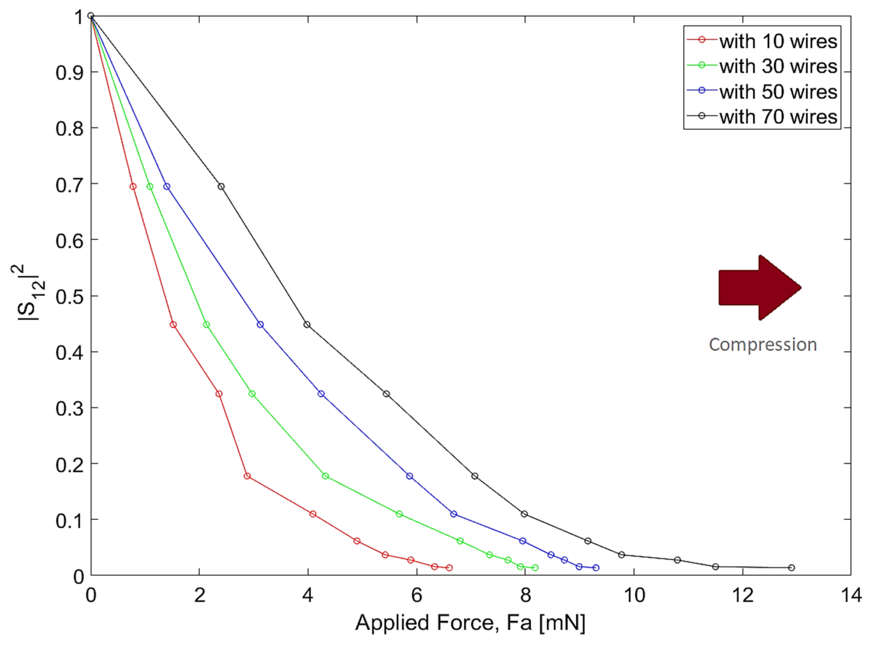
The results for the PTFE host are shown in
Figure 15 and
Figure 16. As can be seen, the curves obtained for this device model are not as linear as we observed in the previous case. When compared to the device built with HDPE, this filter is more sensitive, since it can cover the entire dynamic range with much less applied force (only 21.4% of the required force to fully compress the device built with HDPE). In spite of the linearity issues, we have a linear operating region that allows us to work with reflectances between 0.25 and 0.85, depending on the requirements of the application. For values of applied force greater than 1.20 mN, some saturation of the device response (independently of the curve under analysis) is observed.
Focusing on the scenario, in which we have a filter containing 70 wires per array and a limitation of the applied force of about 1.2 mN, we can see from
Figure 11 that the distance between wires for 1.2 mN of applied force is
d = 18.5 µm. In turn, by analyzing
Figure 7 and
Figure 8, we observe that the resonance frequency of the filter is around 438.4 GHz.
Table 5 shows the filter quality and performance parameters for the scenario under study:
In
Table 6, the relationship between filter sensitivity and the increase in the number of wires is shown, considering the approach used in the previous case:
The filter assembled with PTFE requires less force to be compressed and is very sensitive. However, the data from
Table 6 suggest that the relationship between sensitivity and linearity of the response of the device is the same as was observed for the case where the filter was assembled with HDPE. Given the trade-off between these requirements, we should consider the filter assembled with HDPE, since it has the same good dynamics as the filter assembled with PTFE but has a much more linear response than the latter.
5. Conclusions
This work aimed to study a reconfigurable THz filter design, using frequency selective structures based on metamaterial resonators, so that it can be used in the development of sensor devices. The proposed filter is composed by two arrays of wires to provide greater cancellation of harmonics, higher dynamic range and enhanced frequency selectivity. The resonant effects result from carefully tuning the wire radius and the distance between wires, which can be altered so that only evanescent modes exist in the vicinity of the structure, allowing us to control the energy transmission and reflection. Due to its simplicity, this filter design is especially suited for the implementation of reconfigurable THz filters and optical modulators, since it transits from situations in which it presents a full transparency ( = 0) for a full opacity ( = 1).
Two assembling hypotheses with different thermoplastic polymers materials were analyzed. The choice of these materials was essentially due to the fact that they are relatively easy to compress and exhibit low losses and low dispersion for the frequency band over 0.1 to 5 THz. Numerical simulation using the finite element method allowed us to study the variation of the electromagnetic and mechanical response of the device as compression was applied.
Our results corroborated our theoretical model by proving that it is possible to design a filter with a very good dynamic range and a high sensitivity by following the proposed methodology. The model designed with HDPE presented a quite linear response when compared to the one designed with PTFE, which is more sensitive. This might be explained by the different electromagnetic and mechanical properties of these materials.
For the model composed by HDPE, the required force to be applied to cause a reduction in the distance between wires is four times greater, when compared to the one that is required by the model with PTFE. By analyzing the data from the simulations, it was also determined that the relation between wire spacing and the required current to compress the device is the same, when compared to the amount of force that should be applied to verify a shift on the resonance frequency.


