1. Introduction
Recently, the word
nanolaser has become frequently used in the field of plasmonics. However, it was first applied to a photonic crystal (PC) laser, because its laser mode is confined within a volume smaller than 1 µm
3 by multidimensional Bragg reflection (or point defect, as used in the field). In 1987, Yablonovitch and John conceptualized the photonic band gap and light localization [
1,
2]. In 1994, Meade et al. applied these concepts in planning devices [
3]. In 1999, Painter et al. realized the first laser oscillation under a low-temperature pulsed condition [
4]. Room temperature operation was achieved shortly afterward, and Nozaki et al. reported continuous wave (cw) operation at room temperature in 2007 [
5]. While all these experiments were performed with photopumping, the current injection pulsed oscillation was achieved by Park et al. in 2004 [
6], followed by cw operation by Matsuo et al. in 2012 [
7].
The initial focus of such a small laser was that the spontaneous emission process was modified from that of normal lasers, and the study was conducted by focusing on a point of cavity quantum electrodynamics [
8]. In addition, after the success of current injection cw operation, this novel laser was expected to be a low power consumption light source for optical interconnects [
9]. Nevertheless, in addition to the complexity of the fabrication process, this device is too small to obtain sufficient light output, so that its practical application still remain to be seen. Separately from these studies, Lončar et al. suggested and demonstrated the application of a PC nanolaser for chemical sensors [
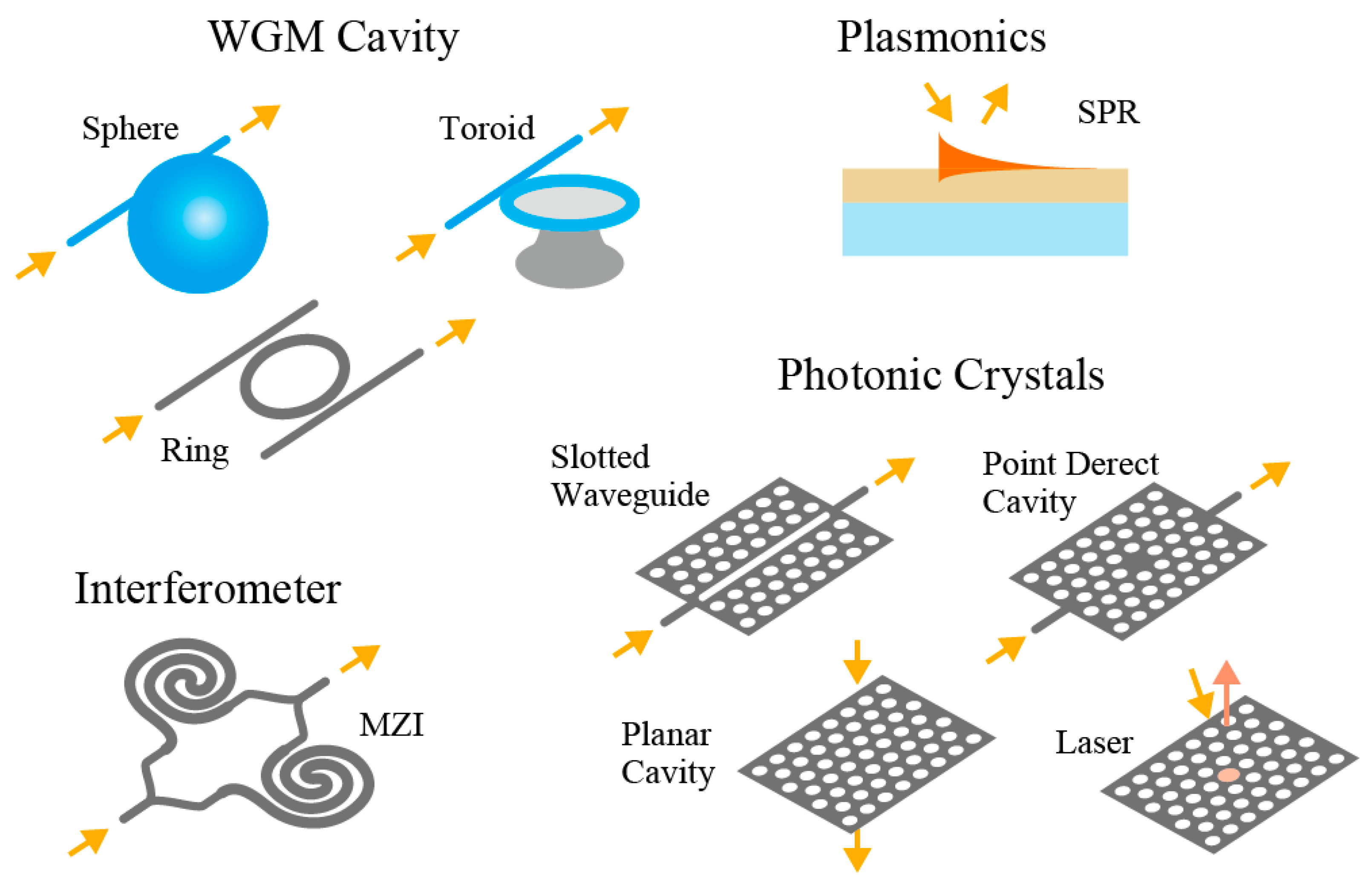
10]. In the nanolaser, the cavity is exposed and, if it goes into contact with a medium, an evanescent field of the laser mode would sense changes (usually, an increase) in the refractive index and change the emission wavelength accordingly (toward longer wavelength). The contact of the medium can be detected by monitoring the laser wavelength. Such a sensing principle of monitoring the resonance wavelength is not limited to nanolasers, as evidenced by many reports on sensor applications of passive microcavities, such as silica whispering gallery mode (WGM) cavities, silicon (Si) photonics, and surface plasmon resonance (SPR), as depicted in
Figure 1 [
11]. Even compared with them, there are possibilities of various applications for nanolasers owing to their simple principle and operation. First, the detection of such refractive index change seemed to be the only sensing principle. It was found afterwards that the electrostatic phenomena induced by ions (we will refer to it as
iontronic effects) at the semiconductor surface also modify the emission intensity and wavelength in nanolasers, indicating the possibility of realizing a more functional and better-performing sensor.
In the paper, we review the GaInAsP semiconductor PC nanolaser and its sensing applications, as depicted in
Figure 2. The conventional refractive index sensing was already reviewed in reference [
12], while this paper further focuses on its iontronic principle and characteristics. Herein, in the next section, we summarize the nanolaser technology.
Section 3 introduces the basic characteristics of sensing based on the principle of refractive index detection and describes typical biosensing examples.
Section 4 presents phenomena observed in the emission intensity, which show an iontronic effect, and provides examples of biosensing using it.
Section 5 also presents superhigh sensitivity in protein sensing obtained by monitoring the wavelength, and
Section 6 finally discusses the possibility that the superhigh sensitivity is also derived from another iontronic effect.
2. GaInAsP PC Nanolaser
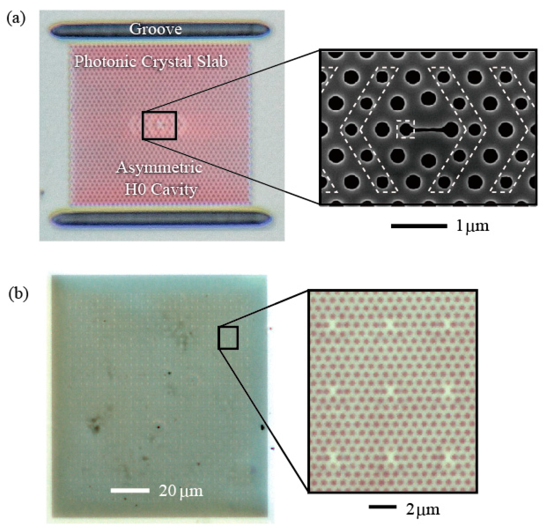
The PC structure used in the nanolasers is a PC slab, wherein circular holes are periodically arranged in a triangular lattice in an air bridge structure with a III–V semiconductor slab floating in the air. Herein, we introduce a point defect that deforms part of the period and use it as a nanocavity. The point defect first used was an H1 type where one hole was removed; however, its Q-value was low and laser oscillation was difficult. To overcome these limitations, the H0 type point defect comprising two or four neighboring holes that are slightly shifted outward was employed [
13]. It allows a passive Q-value of at least 30,000, which are sufficient to cause oscillation, with strong light localization. In addition, a nanoslot was added at the center so that the modal electric field across the slot enhances its amplitude inside the slot by a high contrast in the refractive index (see
Figure 2). This means that the electric field concentrates outside the semiconductor and increases the sensitivity in the sensing applications. Moreover, if sensing is conducted in a solution, the positive temperature coefficient of the refractive index is cancelled by the negative coefficient of water; this is effective for wavelength stabilization and spectral narrowing against environmental temperature changes.
Figure 3a shows a fabricated nanolaser. A semiconductor material frequently used for PC nanolasers is GaInAsP single quantum well layer, which is epitaxially grown on InP substrate and emits light at wavelength of 1.5–1.6 µm. This is because nonradiative surface recombination is smaller in comparison with other semiconductors, and a high internal quantum efficiency is maintained at room temperature, even though the active layer is processed directly. In the fabrication process using electron beam writing and HI based inductively coupled plasma etching, holes (diameter 2
r = 220–240 nm, pitch 500 nm, and lateral shift of two holes at the cavity,
sx = 120 nm) and nanoslots (width
wNS ≤ 60 nm) are simultaneously formed in the GaInAsP layer (total thickness 160–180 nm), and the air bridge structure is formed by undercutting the lower InP substrate by using HCl wet etching. The small number of fabrication steps involved would account for low-cost production of the device in the future, and one-time disposable use would be acceptable. This is a particularly important advantage in biosensing, where sample solutions come into direct contact with the nanolaser.
Pump light at 0.98 µm wavelength is focused to a diameter of 10 µm or less with an objective lens. A good single-mode oscillation is generated at a maximum of 1 mW irradiation power; the effective pump power absorbed around the cavity is 10 μW at most. However, due to a high thermal resistance of the GaInAsP semiconductor and the strong light localization and small effective volume, the thermal resistance of the nanolaser is as large as 10
5–10
6 K/W. Therefore, cw operation becomes difficult if laser threshold exceeds 5 μW at the effective pump power. Although the thermal resistance decreases to 1/10 or less of the original when operated in solution, cw operation causes solution convection, resulting in the fluctuation of pumping and measurement. In biosensing applications, since even a small amount of heat may adversely affect biological samples, pulsed pumping (pulse width = 0.5 µs and repetition frequency = 10 kHz) is employed. With pulsed oscillation, the temporal average power of the oscillation light decreases and leads to a longer measurement time. This situation is improved by directing the emission pattern of the oscillation light toward the light-receiving optical system. The structure of a simple H0 cavity has high symmetry, and a split emission pattern is generated. When a doubly periodic hole size modulation is added to weaken the symmetry of the cavity (see
Figure 3a), upright emission significantly increases, and most far-field components enter the radiation angle within 10°, so that light becomes easily received by the objective lens [
14].
Moreover, photopumping in solution causes etching or oxidization on the nanolaser surface helped by the ions in solution and causes the emission wavelength to drift. To suppress this, the exposed surface of the device is covered with a protective layer. Herein, approximately 3-nm-thick ZrO
2 layer is deposited by atomic layer deposition, which is characterized by excellent film thickness control and step coverage [
15]. Although it is unlikely to operate the device for a long time in sensing applications, no significant deterioration occurs even when it keeps working in water for several days. Specifically, wavelength fluctuation is less than ±20 pm within a few hours. If we take the nanolaser out of the water and into the air, and then put it in the water again to repeat the measurement, the fluctuation increases to less than ±100 pm (hereafter, this value is taken as the wavelength fluctuation of the nanolaser). Regarding the emission intensity, we observed a fluctuation of 0.8 dB and 0.2 dB when the pump level was 1.1 and 2.0 times the laser threshold, respectively.
Note that point defects could be freely placed within the PC slab; therefore, a nanolaser array can be formed if neighboring point defects are placed apart from each other (at least 2.5 µm) so that they are prevented from coupling with each other [
16]. So far, 1000–10000 nanolasers have been integrated (as shown in
Figure 3b), and oscillation with 100% yield has been observed for the 1000 device. The cavity size is designed to be slightly different between neighboring nanolasers so that when their resonance wavelengths are also different, their mutual coupling is suppressed.
3. Refractive Index Sensing
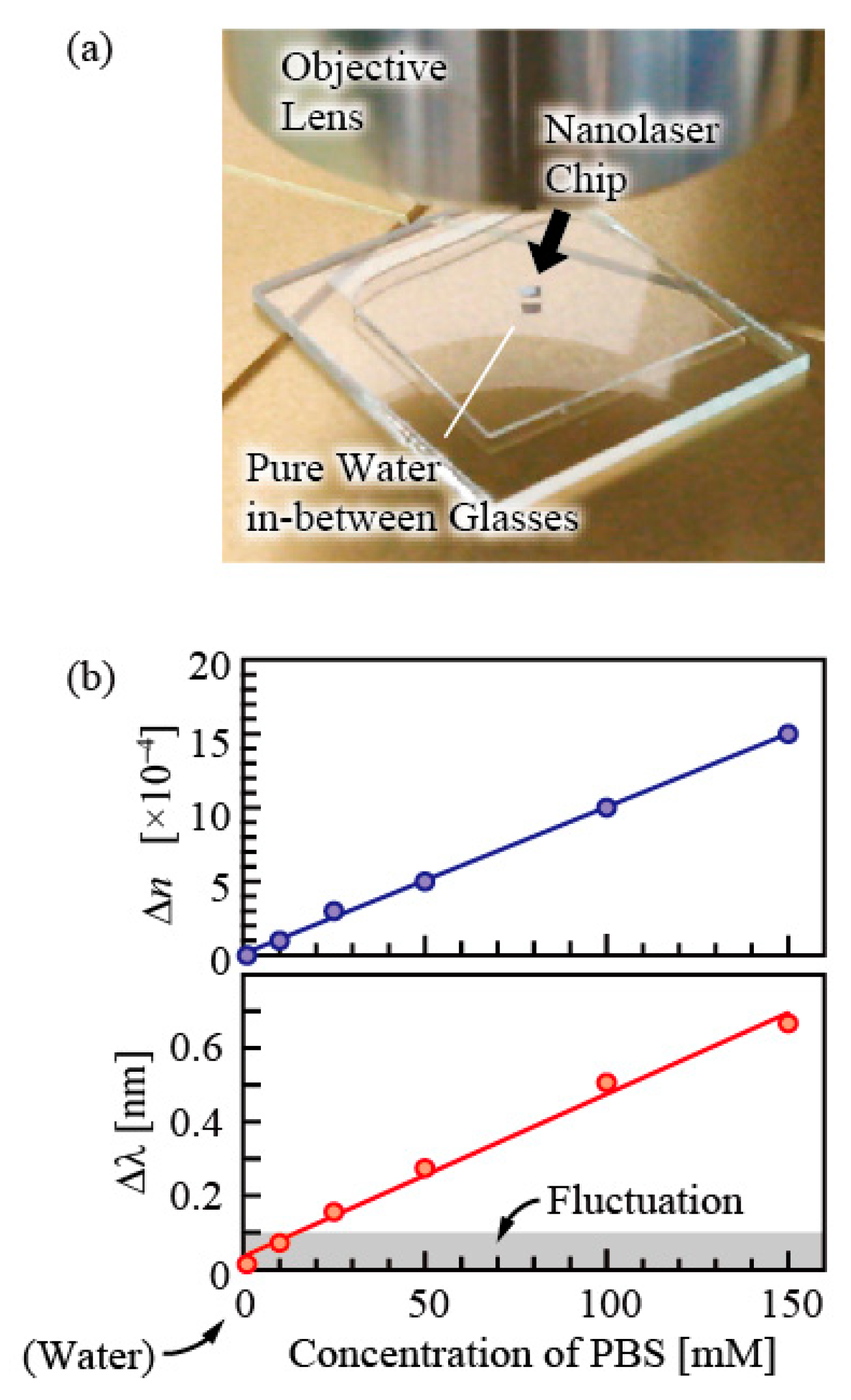
The evanescent field of the laser mode of nanolasers penetrates about 120 nm outside the semiconductor when in the water. When a medium with a high refractive index, such as a bio-molecule, is overlapped with this area, the equivalent refractive index of the mode increases, and the emission wavelength shifts to a longer wavelength. The easiest experiment is the monitoring of the liquid refractive index [
10,
17].
Figure 4 shows an example of such measurement, exhibiting the wavelength shift of the nanolaser measured in phosphate buffered saline (PBS), which is often used in biosensing experiments. In here, PBS was diluted to various levels of concentration and its refractive index was measured using a commercially-available refractometer. Both the refractive index and the wavelength showed liner changes following the changes in concentration, and from their responses, the refractive index of the nanolaser is estimated to be 470 nm/RIU. When the maximum wavelength fluctuation of ±100 pm is taken into consideration, the detection limit becomes 2 × 10
−4. If stabilization is made, fluctuation can be suppressed by about one digit, and the measurement of 10
−5 is possible.
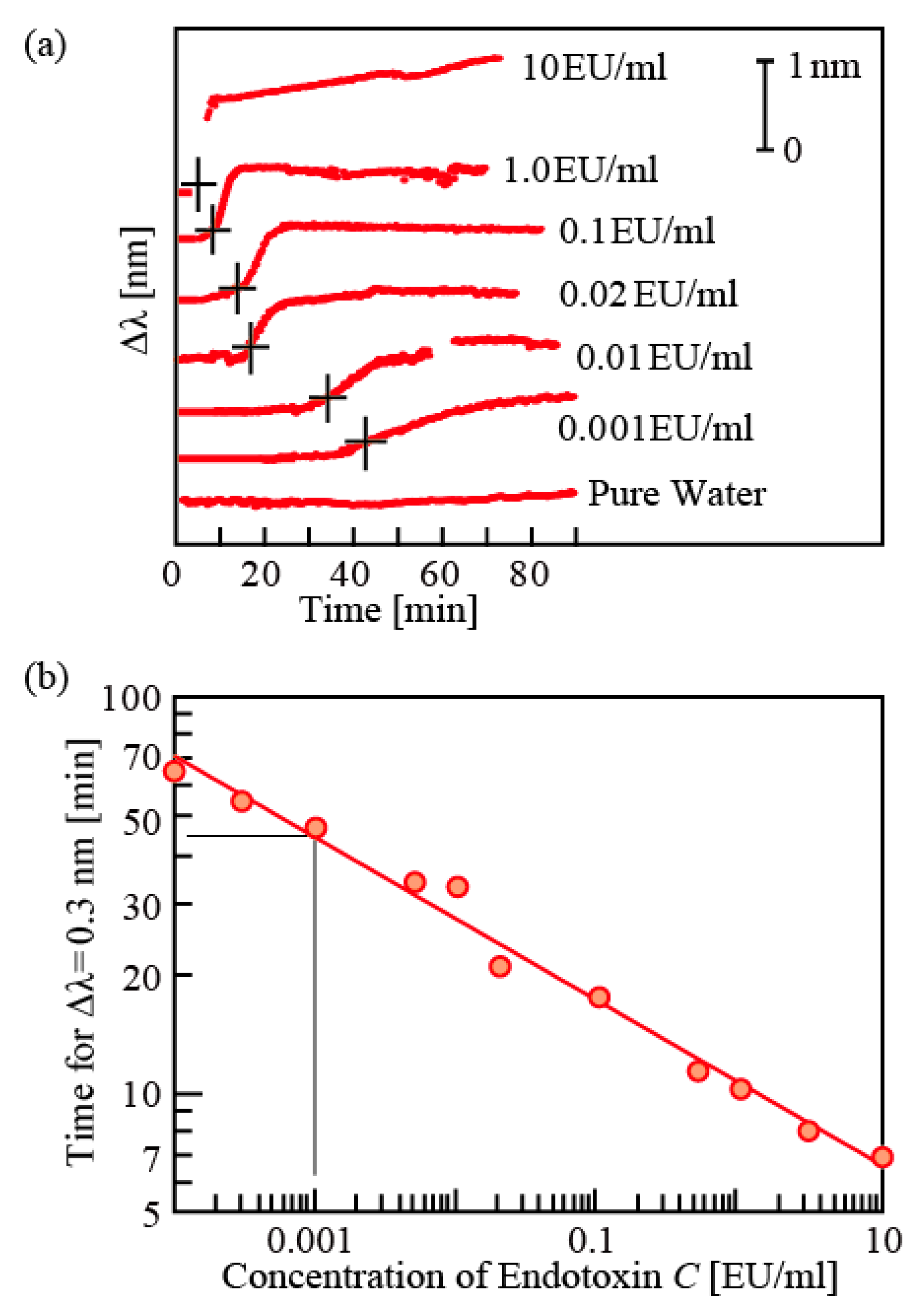
The sensing endotoxin result is shown, as an example of applying this characteristic to biosensing [
18]. Endotoxin is a toxin originating from Gram-negative bacteria and it is widespread in the environment. While it is contained in tap water at a concentration from 1 to 10 EU/mL (EU is the unit for counting the amount of endotoxin), it does not possess any risk to health. However, if endotoxin of the same level of concentration directly enters bloodstream, it can cause fever or sepsis. Thus, strict control of it is obligatory in the case of pharmaceutical agents such as injection solution and dialysate. Currently, the limulus reagent collected from horseshoe crab blood is mainly used for endotoxin tests. As it becomes a gel in reaction to endotoxin, endotoxin can be quantified by recording this process with, for instance, spectrometry.
Figure 5a shows an example of recording this gelation with a nanolaser sterilized by heat. When there is endotoxin and it triggers gelation, the spectrum shifts to the long wavelength side. In addition, the onset and end of gelation appear at the rise and saturation of the wavelength shift. There is a good correlation between the endotoxin concentration and the starting time of wavelength, and if there is a shift of 0.2 nm or more, a correlation that is more than 98% can be obtained. As shown in
Figure 5b, time required for a 0.3 nm wavelength shift exhibited linear relation in the logarithmic plot, and from the fitting curve, 0.001 EU/mL can be detected in approximately 45 min. This is about half of detection time in comparison with common spectrometry, and equivalent to other photonic sensors such as waveguide sensors. As speedy endotoxin detection is particularly required in medical emergencies, such high speed will be a significant advantage.
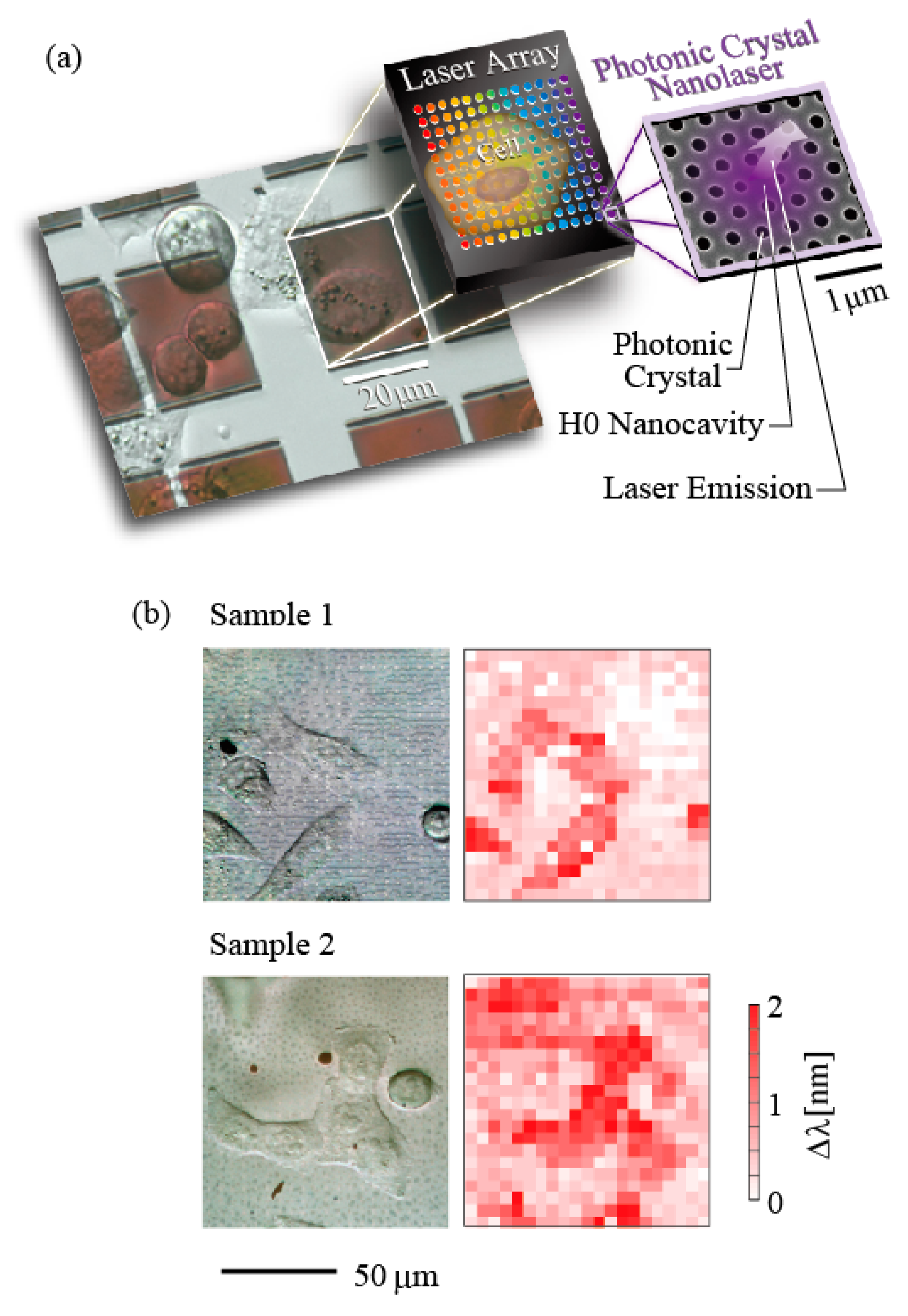
In addition,
Figure 6 shows an image of a cell as an example of biosensing that captures the change in refractive index of the surrounding [
19]. As aforementioned, nanolasers are capable of array integration. Therefore, if a cell is directly cultivated on such an array and emission wavelength of nanolaser is tracked under such a condition, imaging of cell behavior in the form of distribution of refractive index change becomes possible. In an actual experiment, a large-scale nanolaser array is used. However, its surface becomes more than 1 mm square in total, which is too large for the formation of an air bridge structure. Thus, a PC slab is attached to a glass support substrate using dimethylpolysiloxane (PDMS), which is often used in production of micro-fluidic channels, and then InP substrate is removed. Since the nanoslot is neglected for the ease of laser operation and the back of PC was bonded, the penetration of the modal evanescent field is limited to the top and holes of the nanolaser. Thus, the refractive index sensitivity is reduced to 100 nm/RIU. In the experiment in
Figure 5, a chip with such an array was sterilized with ethanol, cleaned with PBS, immersed in a culture solution that contains cervical cancer cell HeLa, and cultivated for 24 h in an incubator. Since the cells tend not to be fixed when ZrO
2 coating is present, coating was omitted in this experiment. With pH = 7.4, the culture solution is almost neutral, and the aforementioned drift is not a significant problem.
Figure 6b shows the view of HeLa observed with 21 × 21 = 441 nanolasers and compares it to the optical microscope image; they are in agreement with each other. As mentioned earlier, the penetration of evanescent field is 120 nm, this wavelength distribution seems to reflect the lower part of the cell, the scaffold, or the extracellular matrix. Herein, it is difficult to obtain information other than refractive index change; however, if the sensitivity discrepancy between nanolasers is calibrated, we can obtain images with a refractive index sensitivity of 10
−4 order. It is expected to be useful for observation of reagent reactions that are difficult to capture with a microscope or for observation of stem cells for which it is difficult to use fluorescent label.
4. Electric Charge Sensing
Similarly to photonic sensors, ion-sensitive field-effect transistor (IS-FET) has been studied as an electronic bio-chemical sensor that does not require fluorescent labels [
20]. Generally, a matter has its own isoelectric point (pI), and is correspondingly charged in solutions near neutrality. Living cells have the same properties, and when a charged living cell is adsorbed to the gate oxide of IS-FET, the channel current changes. Similar phenomena also occur in GaInAsP nanolasers [
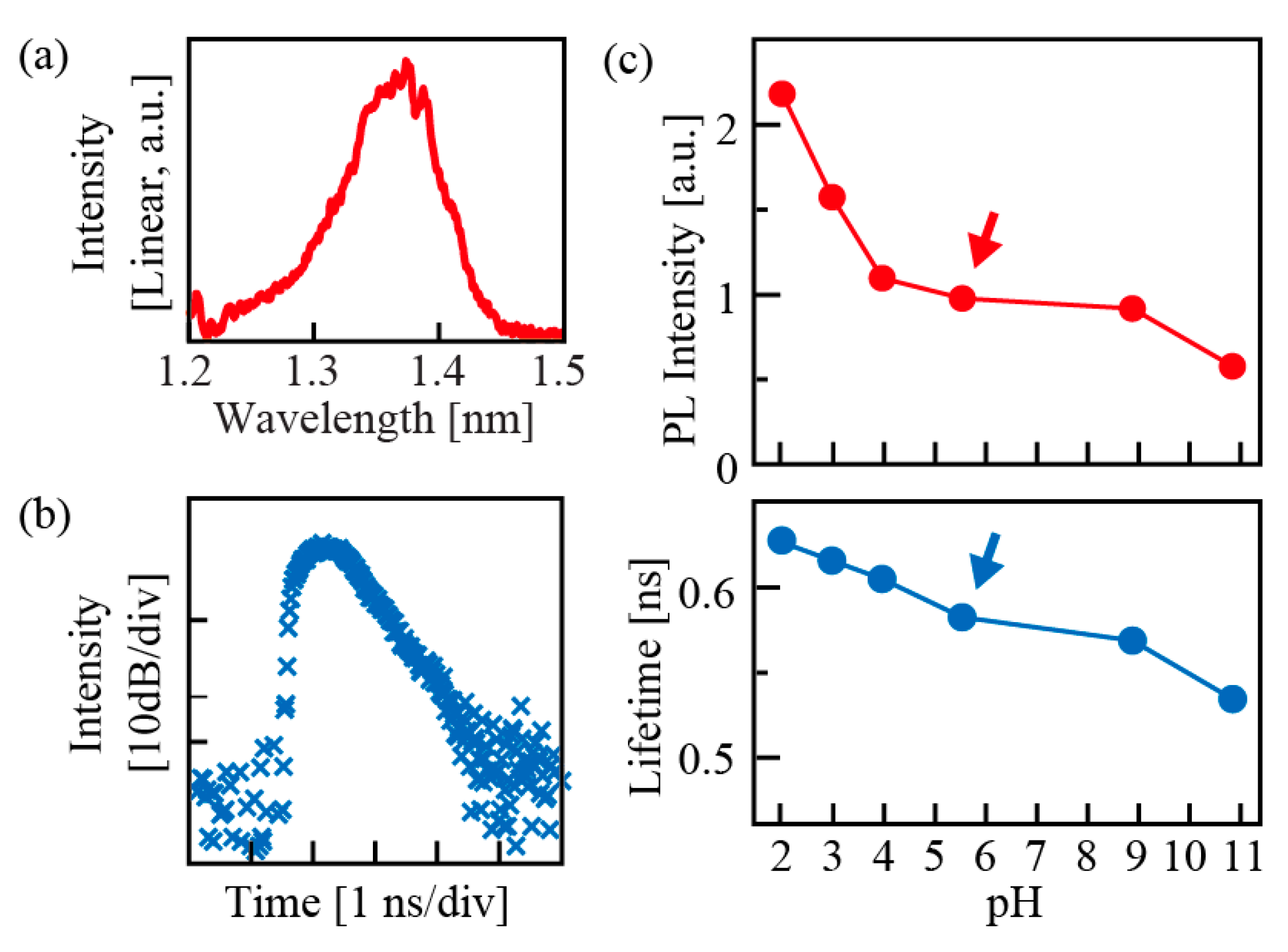
15]. A simple example would be the one where the emission intensity of nanolasers changes when immersed in solution with various pHs. This does not necessarily require a nanolaser structure, as shown in
Figure 7; the intensity and lifetime of photoluminescence (PL) from GaInAsP itself decrease as the pH increases when the semiconductor has the n-type conductivity [
21]. When the semiconductor is changed to p-type, the characteristic is reversed. Furthermore, when ZrO
2 coating is made thicker, pH dependency is weakened and the total light emission intensity is reduced.
With some exceptions, semiconductors are charged by acid dissociation equilibrium of the surface [
22], and the intensity and polarity change due to the relation between pI and pH, and it influences the band shape of electrons inside the semiconductor. For instance, with n-type semiconductor, its surface is positively charged in solutions with pH < pI. At this time, the semiconductor absorbs electrons from ions of the solution, and positive ions gather on the surface of the semiconductor to form an electric double layer. The band of electrons becomes flat, and the holes, which are minority carriers introduced by photopumping, are uniformly distributed in the semiconductor. In contrast, in a solution with pH > pI, the electrons of the semiconductor are deprived by ions of the solution until the Fermi level and redox potential of the solution ions form an equilibrium state. Negative ions concentrate on its surface to form an electric double layer, and a Schottky barrier is formed in the band, where the excited holes exist locally near the surface. Since this reduces the radiative recombination of the semiconductor and at the same time accelerates surface nonradiative recombination, the emission intensity is reduced and the emission lifetime is shortened. As pI of GaInAsP is on the acidic side, a Schottky barrier is formed in a solution near neutrality. Also, when ZrO
2 is made thicker, the tunneling of electrons gets hampered and its interaction with the solution is reduced. Conversely, the Fermi level is fixed to the surface level of the semiconductor and surface recombination is accelerated.
Such characteristics become even more pronounced when the surface is intentionally charged [
15].
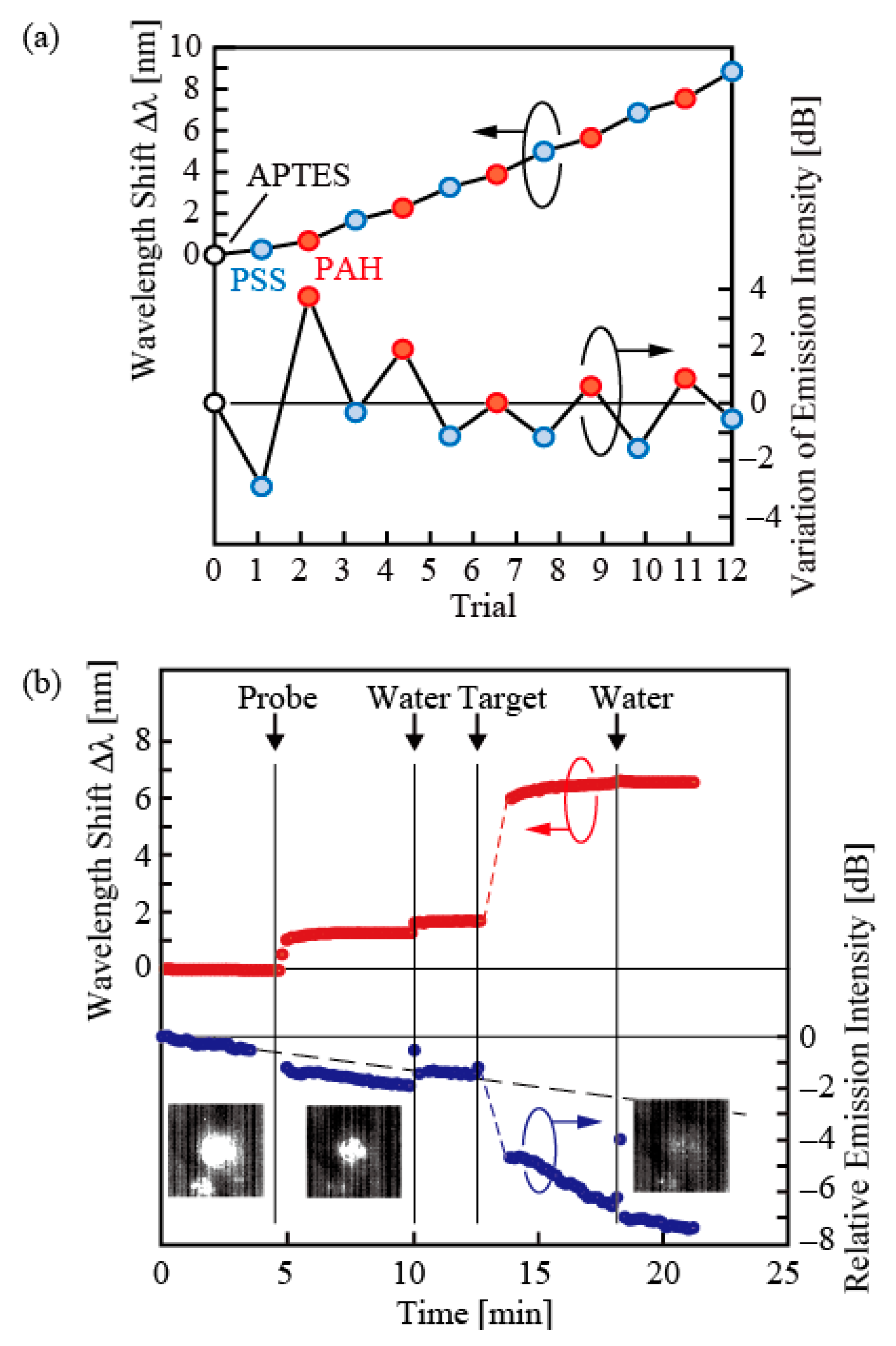
Figure 8a shows the change in the emission intensity and wavelength when (3-aminopropyl) triethoxysilane (APTES), which is a self-organized monolayer that charges positively, is created on the surface of the nanolaser and placed in the PDMS channel, and polystyrene sulfonate, which is a polymer electrolyte that is negatively charged in water, and polyallylamine hydrochloride (PAH), which is positively charged in water, are introduced to be adsorbed alternatively. Such electrolytes have higher refractive indices than water, and when they are repeatedly adsorbed, the wavelength monotonously shifts to long wavelength. In contrast, the emission intensity changes according to the polarity of the charge of the electrolyte; it decreases when the charge is negative and increases when the charge is positive. Thus, sensing the optical and electrical properties is conducted separately but also simultaneously. For biosensing, such a characteristic is effective for examination of deoxyribonucleic acid (DNA). For instance, whether the target DNA to be tested has the same type as that of the reference probe DNA is examined through the light emission from the fluorescent label produced when both form a double strand. With a photonic sensor that does not use a fluorescent label, the target DNA is examined through spectrometry of the wavelength. Herein, DNA originates for instance from the phosphate group, and it is strongly charged negatively in water. When this situation is created on nanolasers, examination can be easily made only from the emission intensity without requiring a fluorescent label or spectrometry.
Figure 8b shows an example of such characteristics. Herein, nanolasers were placed in the PDMS channel, and a single-stranded DNA (12 mer, 2 μM) for the probe dispersed in KCI salt solution was introduced for modification. Through this, the wavelength became long and oscillation intensity decreased further. Then, when a complementary single-stranded DNA that forms a double strand (12 mer, 10 µM) was introduced as a target DNA, the wavelength became even longer and the oscillation intensity decreased further. The emission intensity and wavelength correspond well, indicating that sensing by the emission intensity is possible.
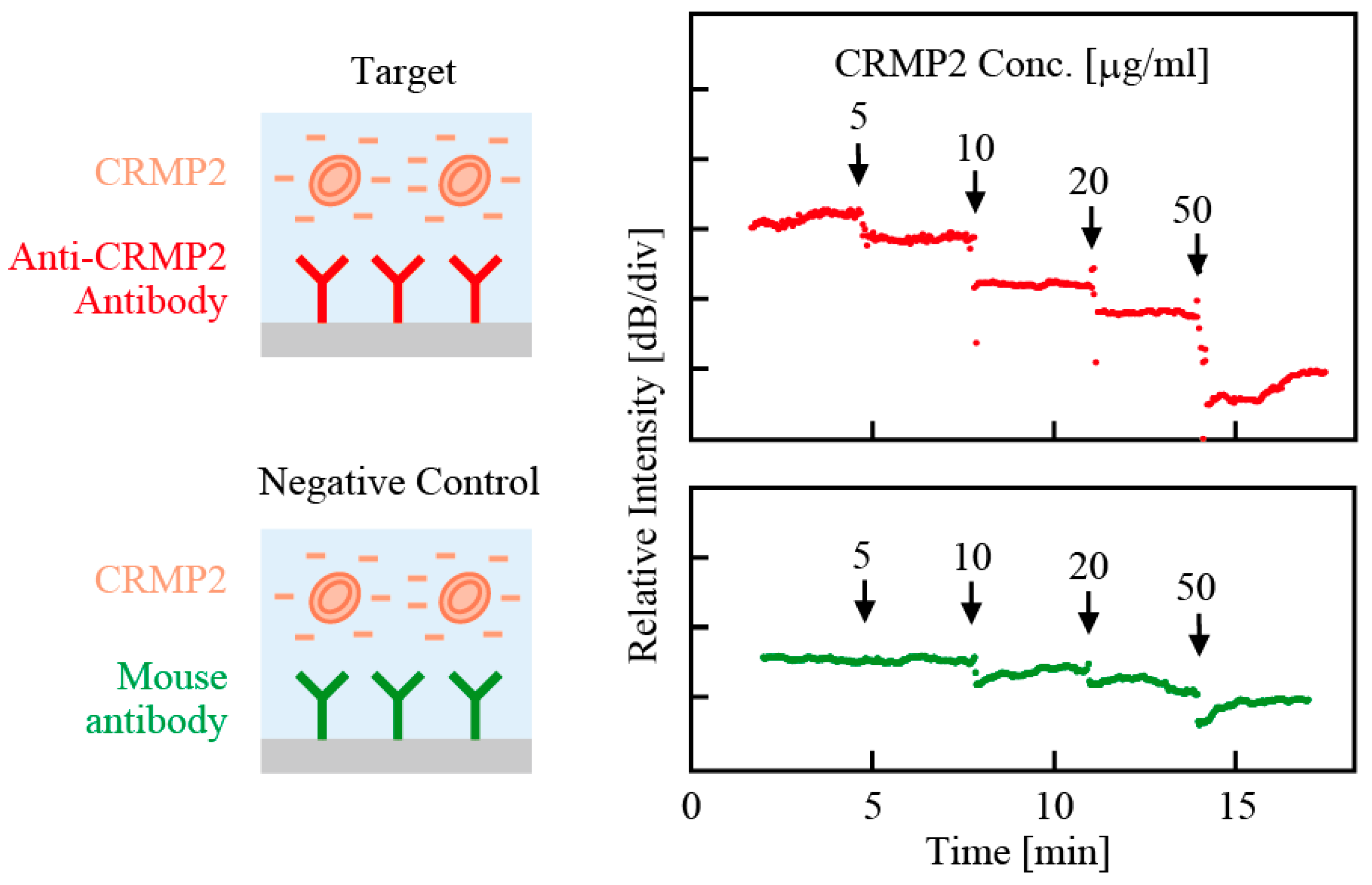
Such a sensitivity of emission intensity was also applied to detecting antigen-antibody reaction of collapsin response mediator protein 2 (CRMP2), which is a promising biomarker candidate for neuropsychiatric diseases existing in peripheral white blood cells [
23]. The CRMP2 sample was prepared as a standard protein and sodium dodecyl sulfate (SDS) was introduced as an anionic surfactant to enhance the net negative charge of the protein. The nanolaser was modified in advance with anti-CRMP2 antibody and then photopumped at a constant power. The emission intensity was monitored during the antigen–antibody reaction. CRMP2 was detected as a decrease in the emission intensity, and a smaller decrease against a non-specific mouse antibody was also confirmed as the negative control, as shown in
Figure 9 [
24]. A standard curve that enables quantification of CRMP2 in the analyte and a lower limit for detection of 3.8 μg/mL that satisfies the requirement for clinical biomarker testing were obtained. Without the requirements of any kind of labels and spectral analyses, this technique allows for simple, rapid, and low-cost biomarker detection.
5. Superhigh-Sensitivity Sensing
In the case of DNA, even if it is a small amount, the same DNA can be reproduced and increased by repeating the polymerase chain reaction; therefore, there is little demand for high-sensitivity sensing. In contrast, there is no similar method to increase protein; therefore, high sensitivity is required to detect a small amount. Sensing of a protein that acts as a sign for a specific disease (biomarker) will have a large impact on health check and treatment. However, samples such as blood generally contain a large amount of contaminant other than the target protein (for instance with human blood, serum albumin with concentration higher than 1 mM), and they prevent detection of the target protein whose amount is orders of magnitude smaller. Generally, antigen-antibody reaction is used for selective detection of a specific protein. By attaching the antibody of the target protein on the surface of the sensor in advance, only the target protein is detected through the antigen-antibody reaction. However, when there is a large amount of contaminant, they cause physical adsorption through Van der Waals force or electrostatic interaction. Suppressing such nonspecific adsorption and capturing only the target protein are major challenges of protein detection. The degree of adsorption is expressed by an affinity constant KA, and when compared to KA of physical adsorption, ≈105 M−1, the antigen–antibody reaction is three to six orders larger at 108–1011 M−1. However, the concentration of target protein is normally of the order of nM to sub pM and six to ten orders of magnitude smaller than albumin. Therefore, it is necessary to either improve KA by finding a better-performing antibody or by further limiting physical adsorption. The former is not easy as it depends on the contingency of the discovery of a new antibody. Meanwhile, the latter includes suppression of physical adsorption by surfactant and blocking of physical adsorption by intentionally absorbing another protein with the antibodies.
Currently, enzyme-linked immuno-solvent assay (ELISA), which is a kind of chemical methods, is widely used for examining proteins [
25]. This method requires high-cost chromogenic substrate and many working processes are involved, and the automated equipment is expensive. In contrast, photonic sensors have the advantage of low cost and not requiring chromogenic substrate. However, it must at least surpass the performance of ELISA to be practically applied. For instance, ELISA can detect prostate specific antigen (PSA), which is a representative cancer marker, down to concentrations as low as 0.3 pM. The detection limit of many photonic sensors based on the principle of refractive index sensing is at best sub nM; therefore, they cannot replace ELISA. Moreover, physical adsorption increases close to the concentration of 10–100 nM; therefore, the effect of the antigen-antibody reaction becomes relatively small and selective detection becomes difficult.
Nanolasers possess superhigh sensitivity that is not available from other photonic sensors. In detecting proteins, the nanolaser surface is functionalized by, for example, APTES followed by glutaraldehyde (GA), an immobilizing material that causes a crosslinking reaction. With such functionalization, an experiment was conducted to adsorb and sense three types of proteins [
26,
27,
28]. The first type was bovine serum albumin (BSA), which is a generic protein. This was chemically adsorbed on GA as is (
KA ≈ 10
7 M
−1). The second type was streptavidin (SA), which is also a generic protein. Biotin, which is a type of vitamin that has strong specific binding with SA (
KA ≈ 10
15 M
−1), was attached on GA, and SA was introduced and adsorbed to it. The third type was anti-PSA antibody, which was modified on GA and antigen–antibody reaction when PSA was triggered (
KA ≈ 10
8–10
9 M
−1). Each protein was diluted with pure water into many different concentrations through pipetting. The concentrations of PSA were verified down to 0.3 pM with ELISA, error was corrected, and the concentrations below that were estimated from the repetition of dilutions. Each sensor was immersed in solution for about 1 h, and the wavelength was measured in pure water after rinsing it with pure water.
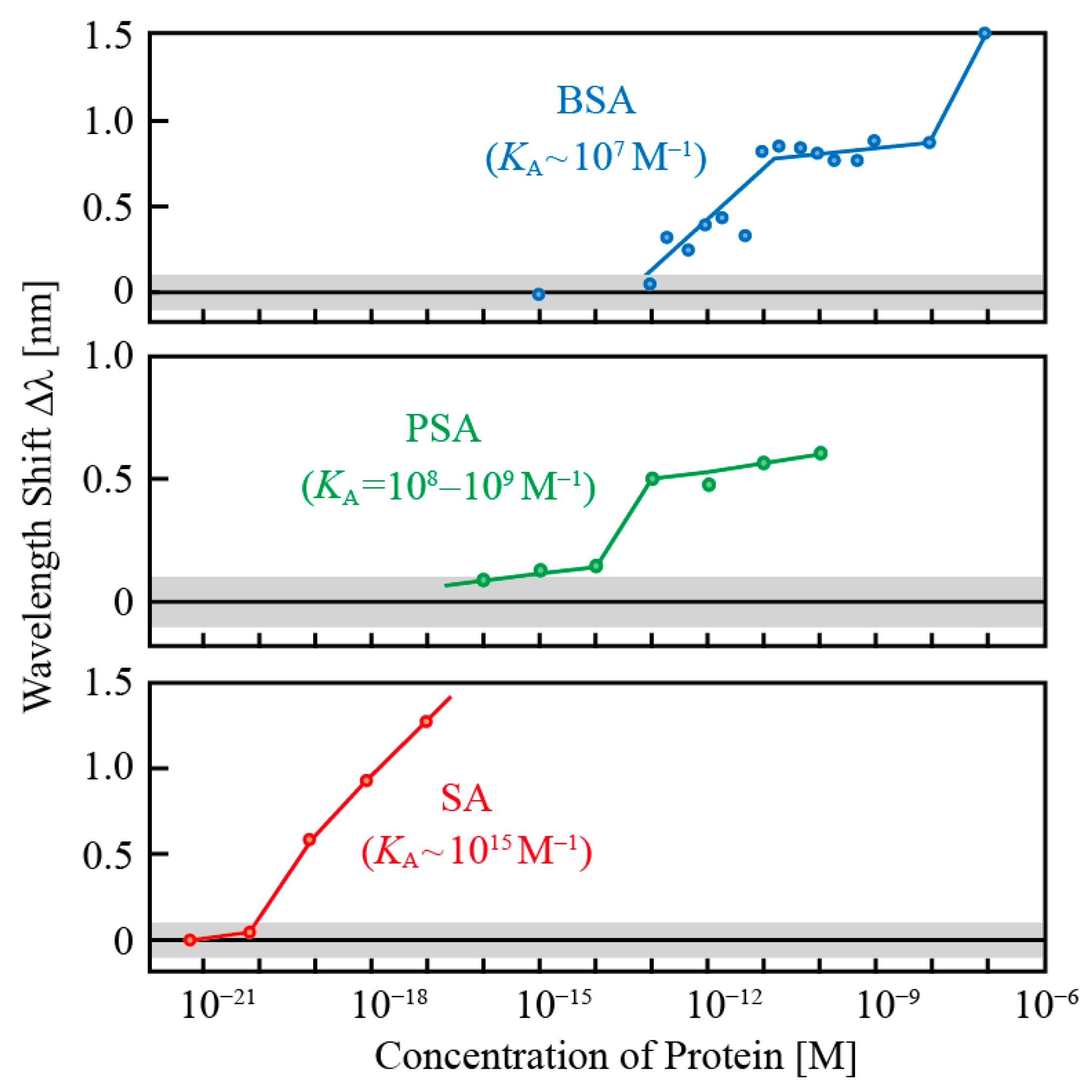
Figure 10 shows an example of sensing characteristics at low-concentration regions. Sensing each protein showed a wavelength shift after the limit concentration that reflects differences in
KA. Although precise discussion of values is difficult owing to the fluctuations between tests and devices, there is qualitative reproducibility. A shift was observed for the chemical adsorption of BSA, which has the lowest
KA, from sub pM, the SA-biotin specific binding from sub aM, and PSA from sub fM, respectively. The concentrations are several orders of magnitude lower than the region above 10 nM expected from refractive index sensing, and therefore, the origin of this shift is different from that appeared for the adsorption of high concentration electrolytes and DNAs in
Figure 8. The SA detection did not show such a wavelength shift at an extremely low concentration if biotin modification was removed. In the PSA detection, wavelength shift was significantly reduced when mouse antibody was modified instead of anti-PSA antibody. Moreover, when BSA was introduced as a contaminant, selective detection of SA or PSA was successful even when the concentration of BSA was increased 10
10 times to 10
13. For these experiments, surfactants, such as Tween 20 or ethanolamine, were also introduced as respective solutions to limit non-specific adsorption of BSA.
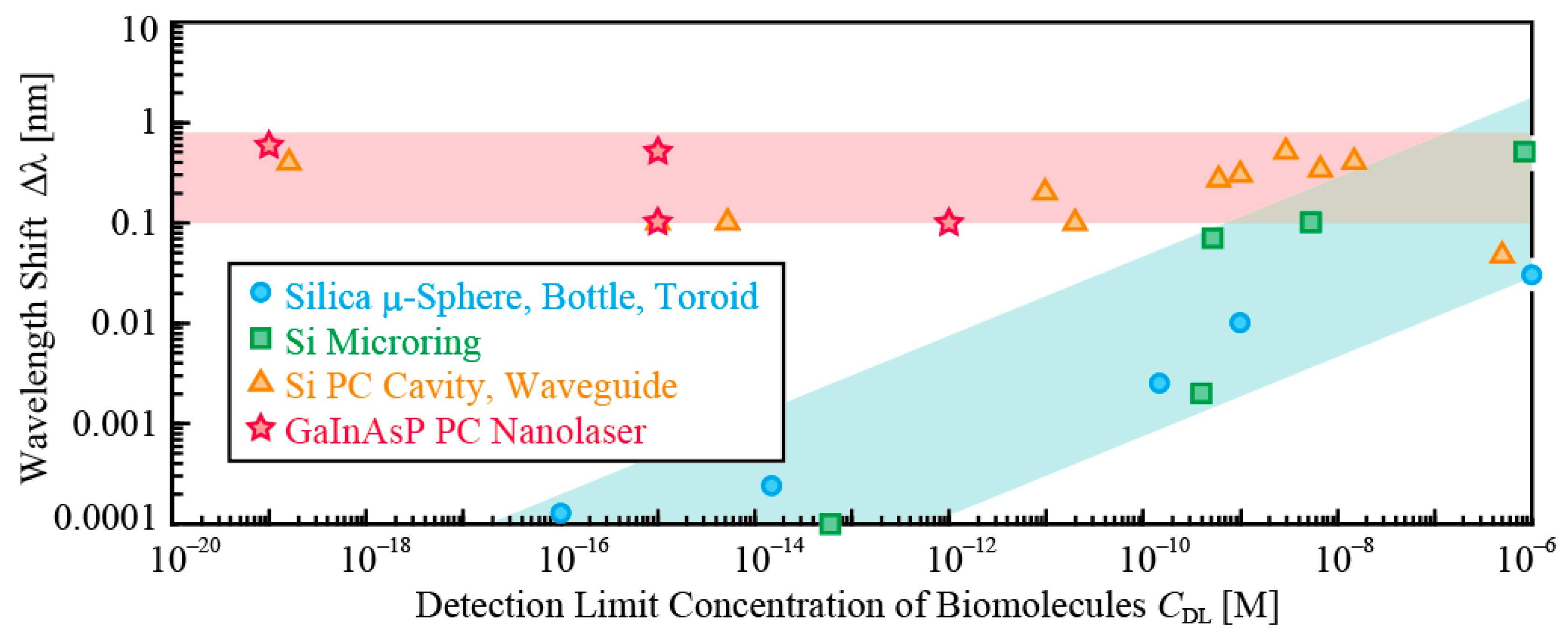
Table 1 lists
KA of proteins and detection limit concentration
CDL of various label-free biosensors reported in references and compares it with the performances of the nanolaser sensor [
12]. Assuming that
CDL decreases during the adsorption with large
KA; therefore (
KACDL)
−1 was defined as a figure-of-merit (FOM). A large FOM can be observed through localized surface plasmon resonance (LSPR), microtoroidal cavity, PC nanolaser and Si nanowire FET. However, apart from nanolaser, the other three lack systematic data, and sensing examples using samples with contaminant, and they are considered to show unstable results. In contrast, nanolaser is easy to conduct a systematic measurement with using many devices. The abovementioned result with PSA was statistically verified through the wavelength shift of six experiments held on different days using 10 to 25 nanolasers [
28].
6. Iontronic Wavelength Shift
Section 4 and
Section 5 have shown that, in the GaInAsP PC nanolaser, the emission intensity has the sensitivity to the electric charge of surface ions and the emission wavelength exhibits the sensitivity to an extremely low concentration of biomolecules. Therefore, in this section, we discuss the possibility that the wavelength shift also occurs due to the iontronic effect. Actually, many groups have observed wavelength shifts in photonic sensors based on optical resonance, which cannot be explained by the simple principle of measuring the refractive index of biomolecules, as summarized in
Figure 11 [
29], although the authors have never indicated and discussed their irregularity and their mechanism. In
Figure 11, sensors using silica cavities and Si microrings exhibit a reasonable decrease of the wavelength shift for lower concentration of biomolecules, although the shifts do not necessarily yield the linear relation with the concentration of biomolecules because the biomolecules used for their experiment were not the same. In contrast, Si and GaInAsP PC devices show similar shifts for concentrations in the range of more than 10 orders. Another phenomenon in these PC devices, which has been reported in some papers but almost neglected by their authors themselves, is a large wavelength shift observed for a small amount of antigen-antibody reaction, which is even larger than that for the simple adsorption of a large amount of antibody. These results suggest that the principle of producing the shift for such low concentrations could be different from the refractive index of biomolecules.
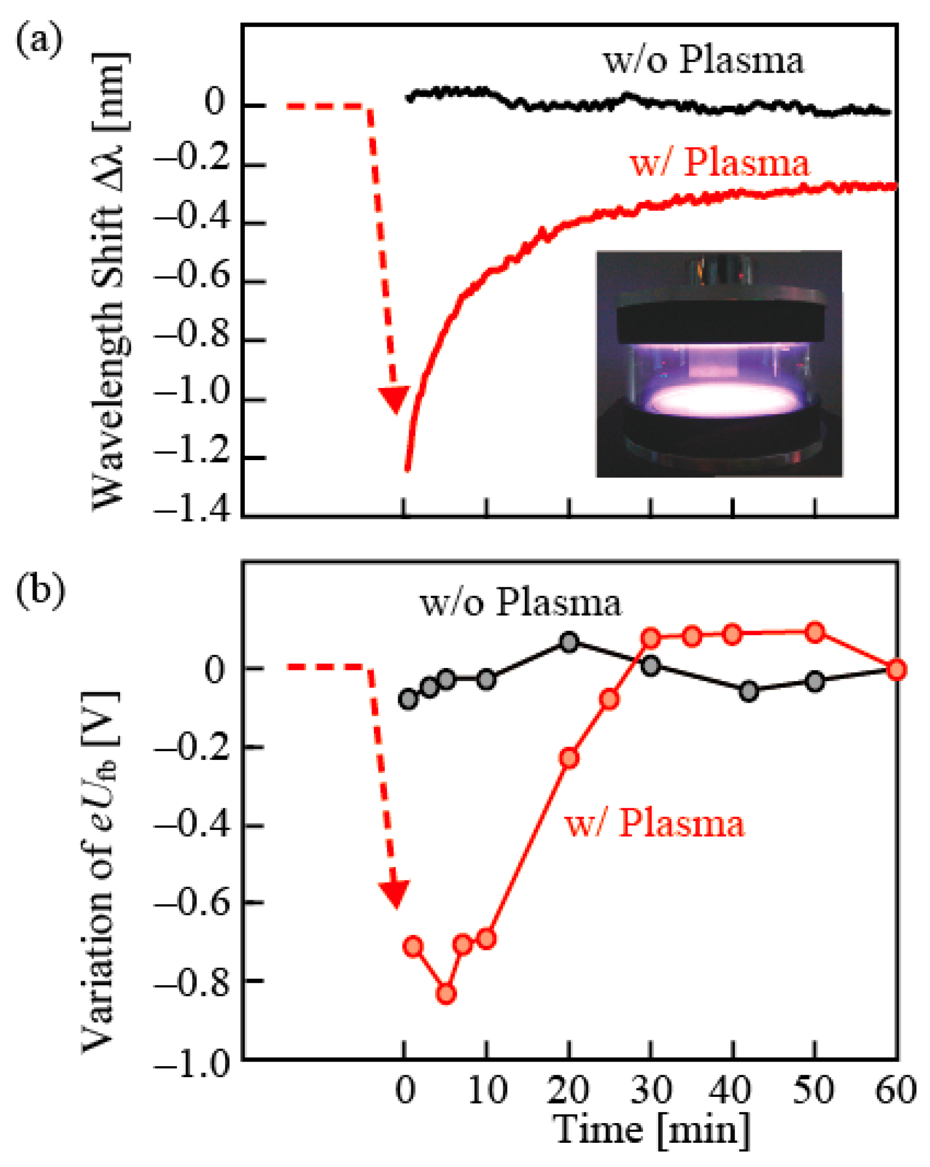
An experiment that demonstrated the principle of the iontronic sensing was the temporal wavelength shift after air plasma exposure of the nanolaser, as shown in
Figure 12 [
29]. Just after the plasma exposure, the wavelength shifted to the short wavelength side in water, but it returned gradually toward the initial wavelength, although the final wavelength after saturation was slightly shorter than the initial wavelength due to the oxidation of the nanolaser surface. After the plasma exposure, similar gradual variations were observed in the negative increase of the flatband potential of GaInAsP, which was measured by an electrochemical measurement (Mot-Schottky plot) and in the positive shift of the zeta potential, which was measured from the Doppler shift of laser light irradiated to microspheres adjacent to the device surface. They agree well to the behavior of the wavelength. These are considered to be the observations of a phenomenon that (1) the chemical bonding of surface oxides is separated by the plasma; (2) positively charged ions attract the electrons in the n-type GaInAsP and a Schottky barrier is formed with the increased flatband potential; (3) negatively charged ions form an electrical double layer (EDL) in water with H+ as counter ions; and (4) the surface charge is gradually neutralized by the OH group. In this process, we can consider two mechanisms that change the emission wavelength. One is the plasma effect of excited carriers that are captured by the Schottky barrier without relaxation and the other is the Pockels effect of water in the EDL [
30], both of which are confirmed theoretically to be candidate reasons that reduce the refractive index of GaInAsP and water, respectively, and shift the emission wavelength.
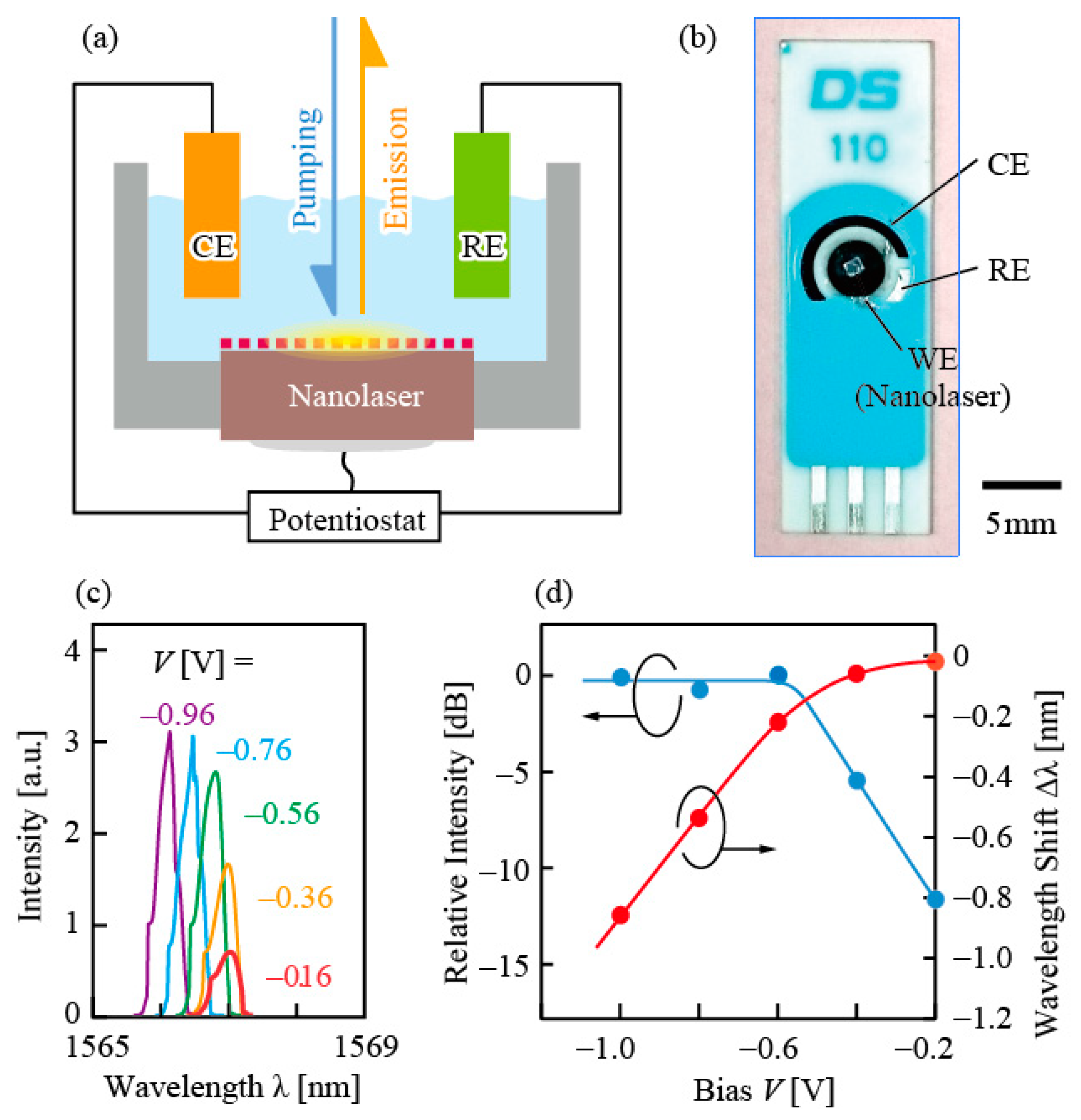
To further confirm the iontronic effect, a standard three-electrode photo-electrochemical circuit was fabricated with the nanolaser as a working electrode and the emission intensity and wavelength were controlled electrically by the bias voltage
V, as shown in
Figure 13 [
31]. It was estimated from the measurement of the flatband potential and rest potential that the equilibrium condition between the Fermi level of the n-type GaInAsP and the redox potential of hydrogen ions in water was given by
V ≈ −0.6 V. Therefore,
V > −0.6 V worked as a reverse bias and enhances the Schottky barrier, while
V < −0.6 V, a forward bias and flattens the barrier. The emission intensity decreased under the reverse bias condition. This is consistent with the discussion in
Section 4; the internal quantum efficiency of excited carriers is degraded by the surface recombination, which is accelerated by a high Schottky barrier. In contrast, the wavelength shift appeared under the forward bias condition, where the electrons in the GaInAsP are accumulated at the surface and the bias voltage is directly applied to the EDL. Therefore, the Pockels effect might be the origin of the wavelength shift.
7. Conclusions
GaInAsP PC nanolasers are fabricated and operated easily and can be useful and disposable biosensor chips. When the principle of the refractive index sensing is employed, the nanolaser can measure a 10−4 order refractive index variation of attached medium such as liquids without stabilization. This operation mode enables us to detect biomolecules of nM order concentrations, monitor the gelation process of the LAL assay for endotoxin, live cell imaging using a large-scale nanolaser array, and so on, via the spectral analysis. When the principle of the emission intensity to be modified by the surface ions is employed, the nanolaser enables us to measure pH and detect the biomolecules in the similar concentration regime only by using a photopump source and photodiode. Due to its simple setup and sensing procedure, this operation mode has the potential of becoming an alternate biomarker detection method of ELISA.
The most attractive and unique phenomena of the nanolaser is the super-sensitivity in the emission wavelength to an extremely low concentration of biomolecules. Various observations indicated that this wavelength shift also could be arising from the iontronic effect, but the mechanism is not the necessarily same as that for the emission intensity variation. The possible mechanisms are the plasma effect of carriers trapped by the Schottky barrier and the Pockels effect at the EDL induced by surface ions. The mechanism that the adsorption of a small amount of biomolecule strongly influences the Schottky barrier and/or EDL is an issue of great interest. It is not only valuable for the nanolaser biosensor but also for PC passive sensors and ISFETs, which are thought to operate via a similar phenomenon.


