Transfer Printed Nanomembranes for Heterogeneously Integrated Membrane Photonics

 , ,
, , 
Abstract
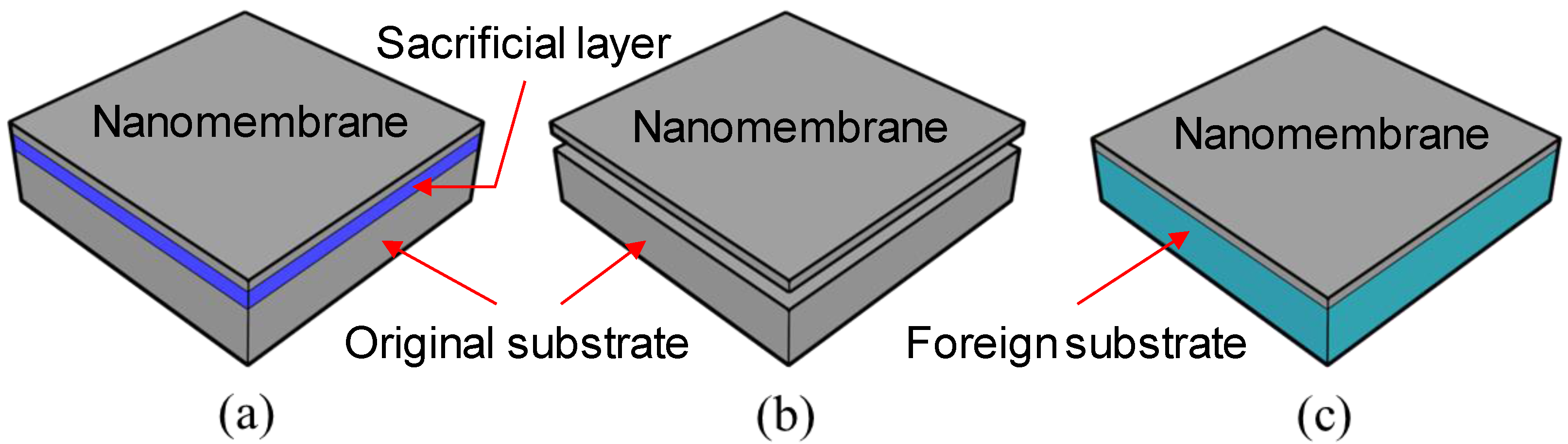
:1. Introduction

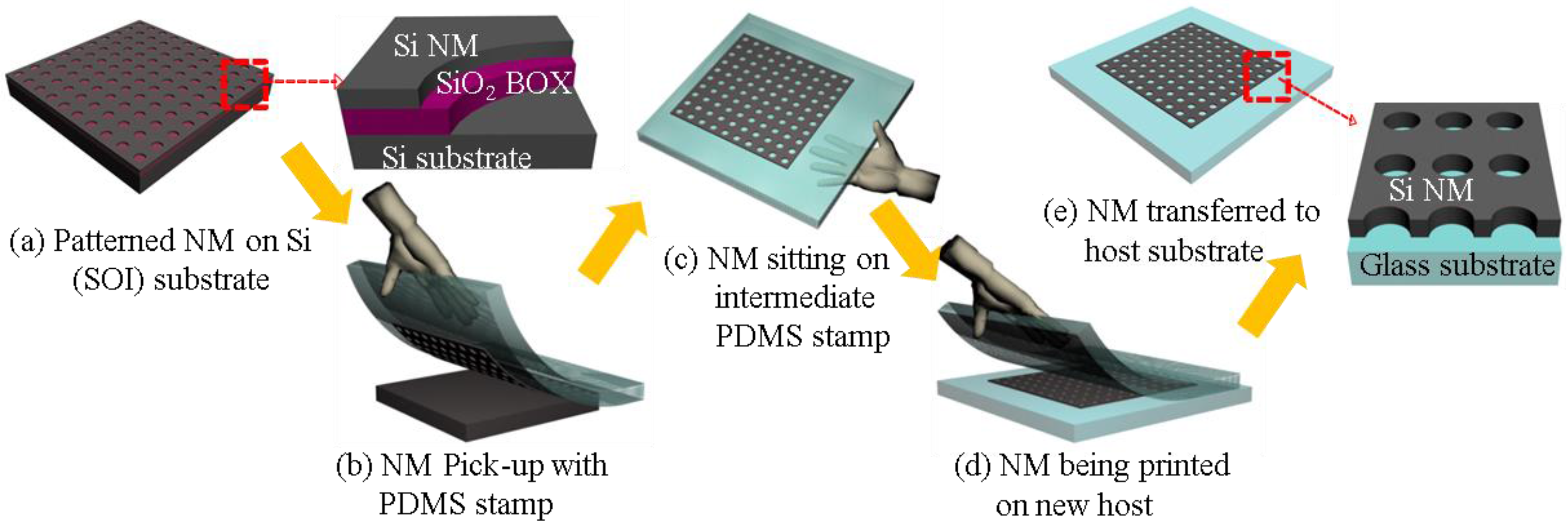
2. Transfer Printing of Silicon NM
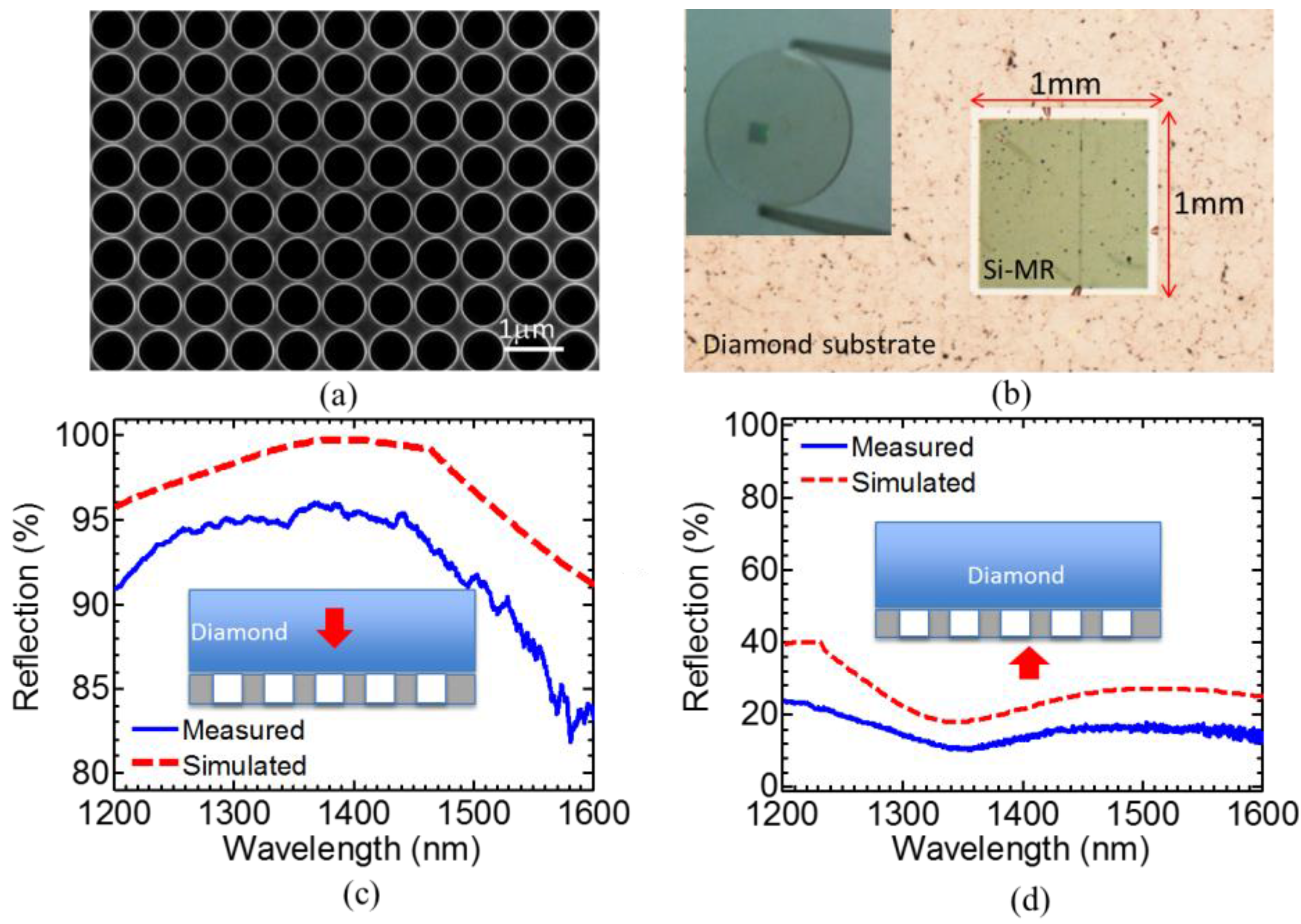
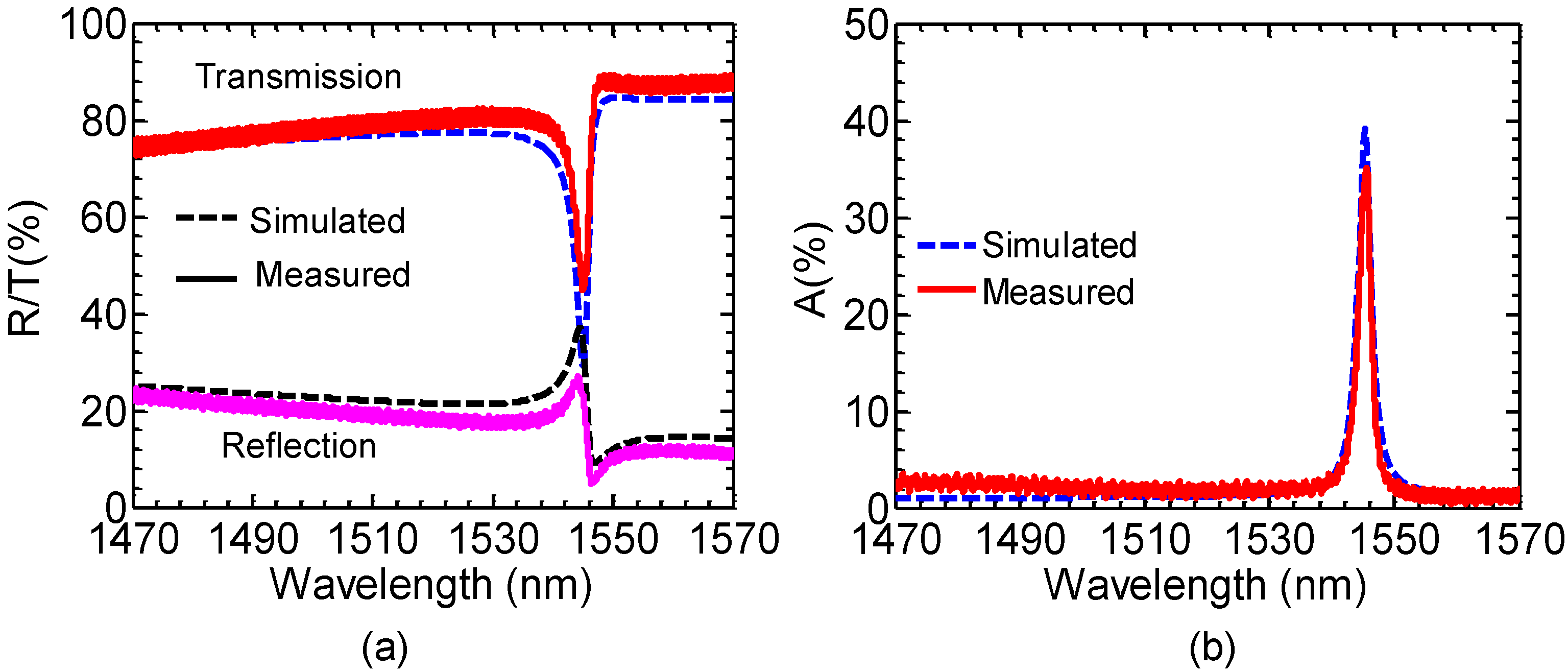
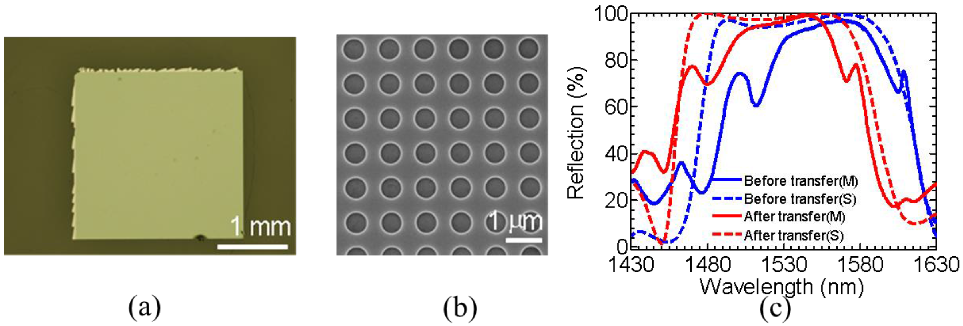
2.1. Demonstration of SiNM Reflectors on Glass/Diamond


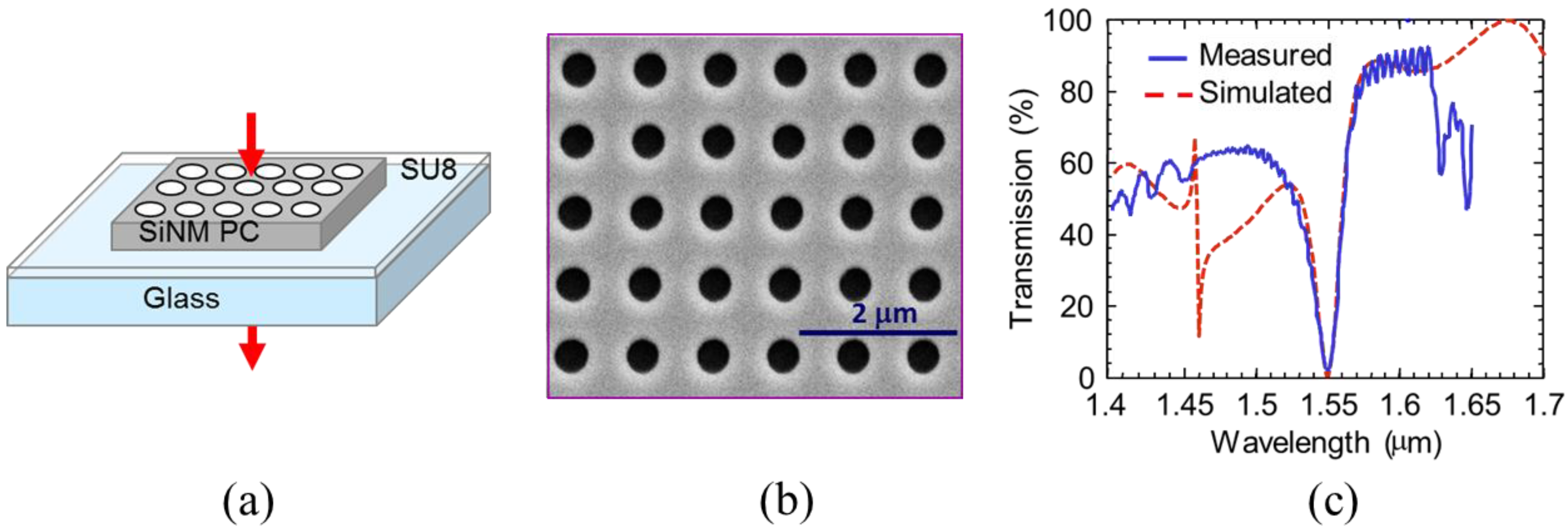
2.2. Demonstration of SiNM Fano Filters on Glass/PET
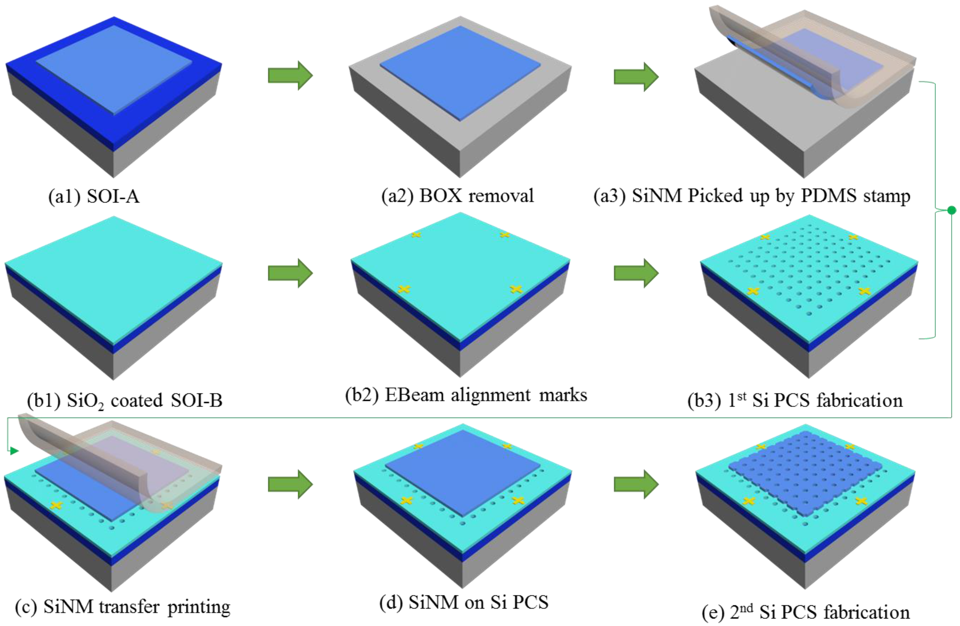
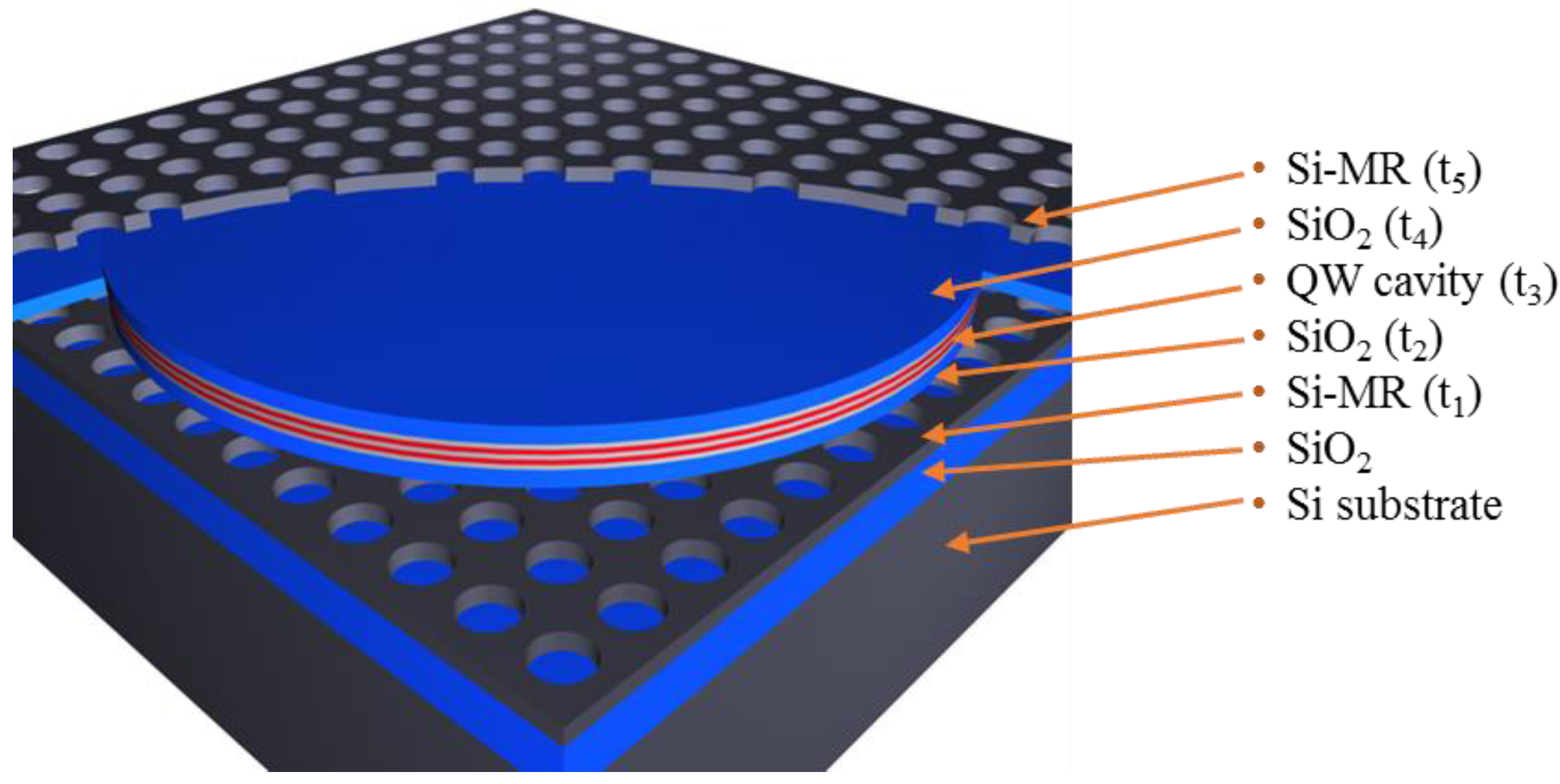
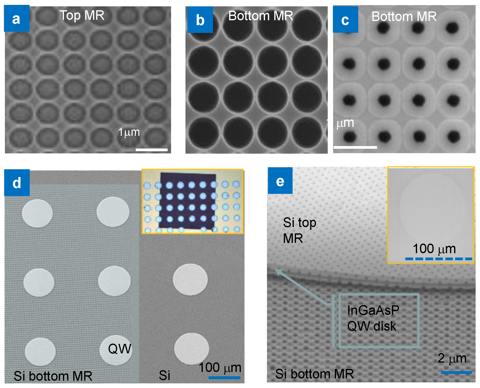
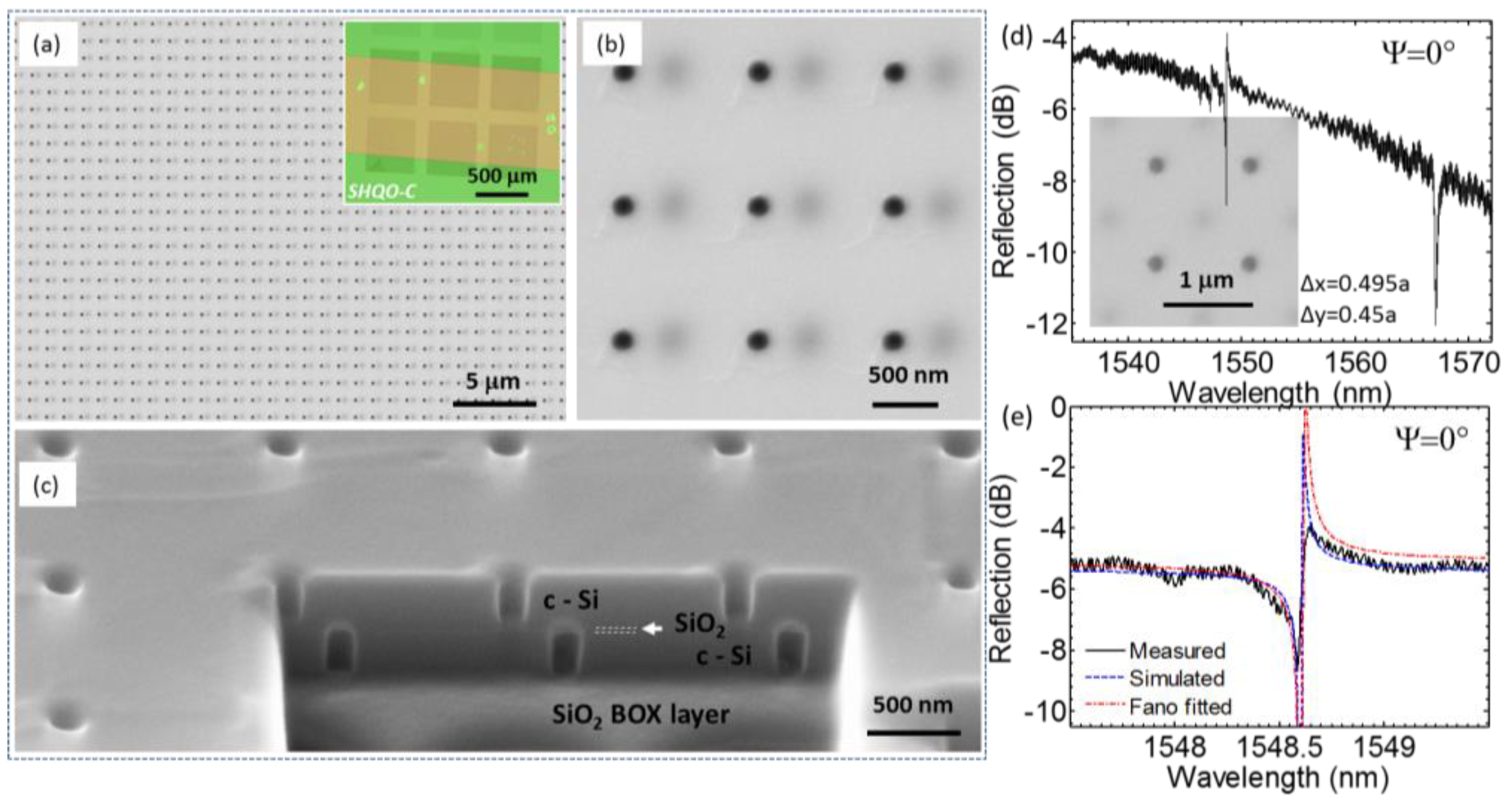
2.3. Demonstration of Coupled Double-Layer SiNM Fano Filters with Shifted Lattice

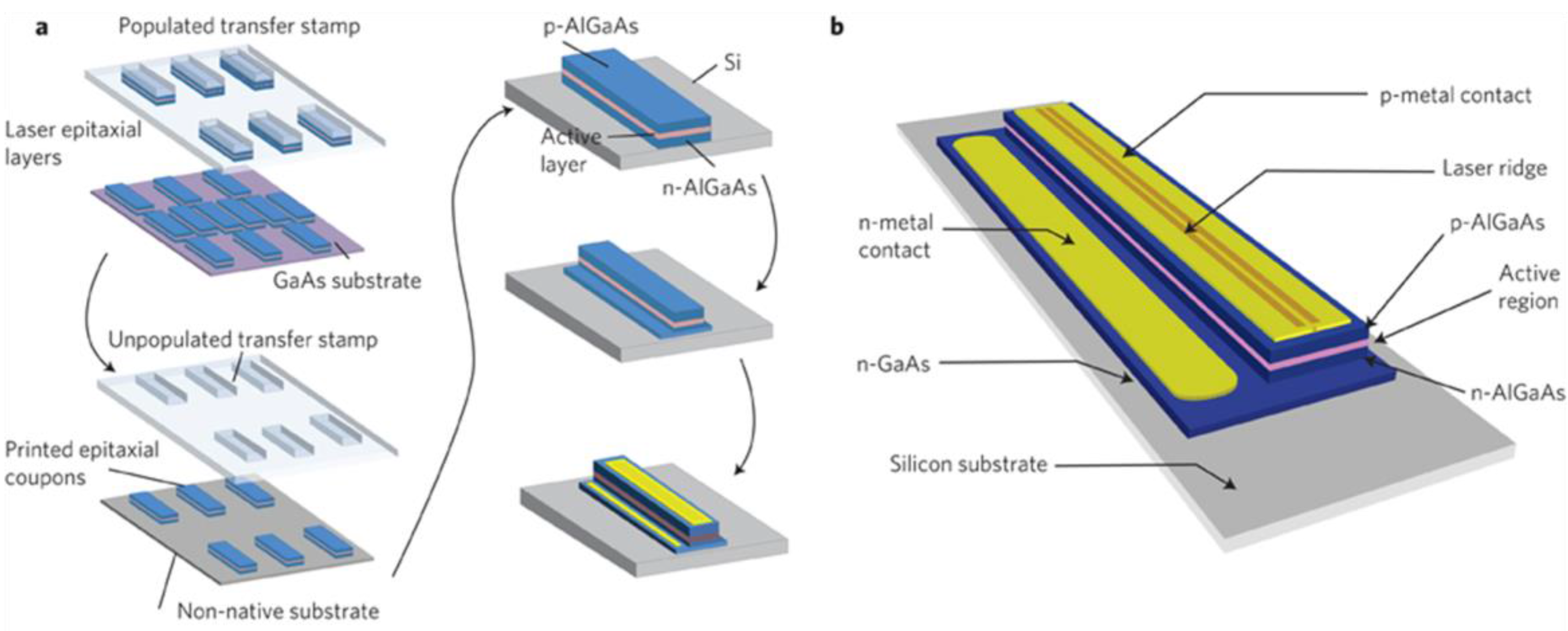
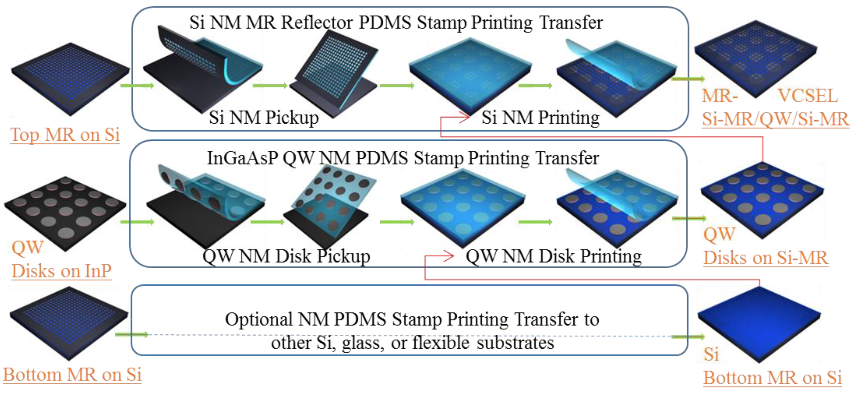
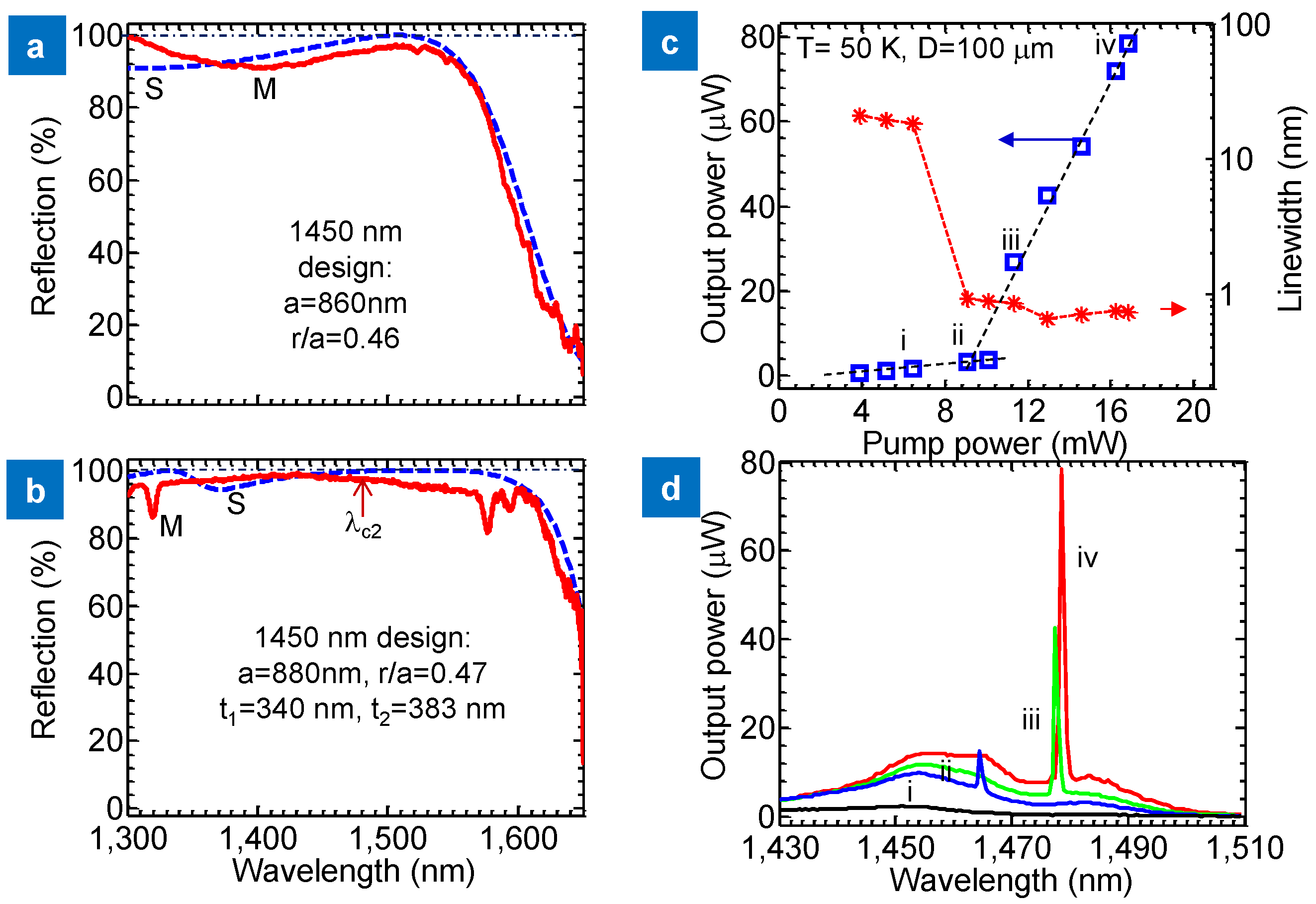
3. Transfer Printing of III-V Group NM


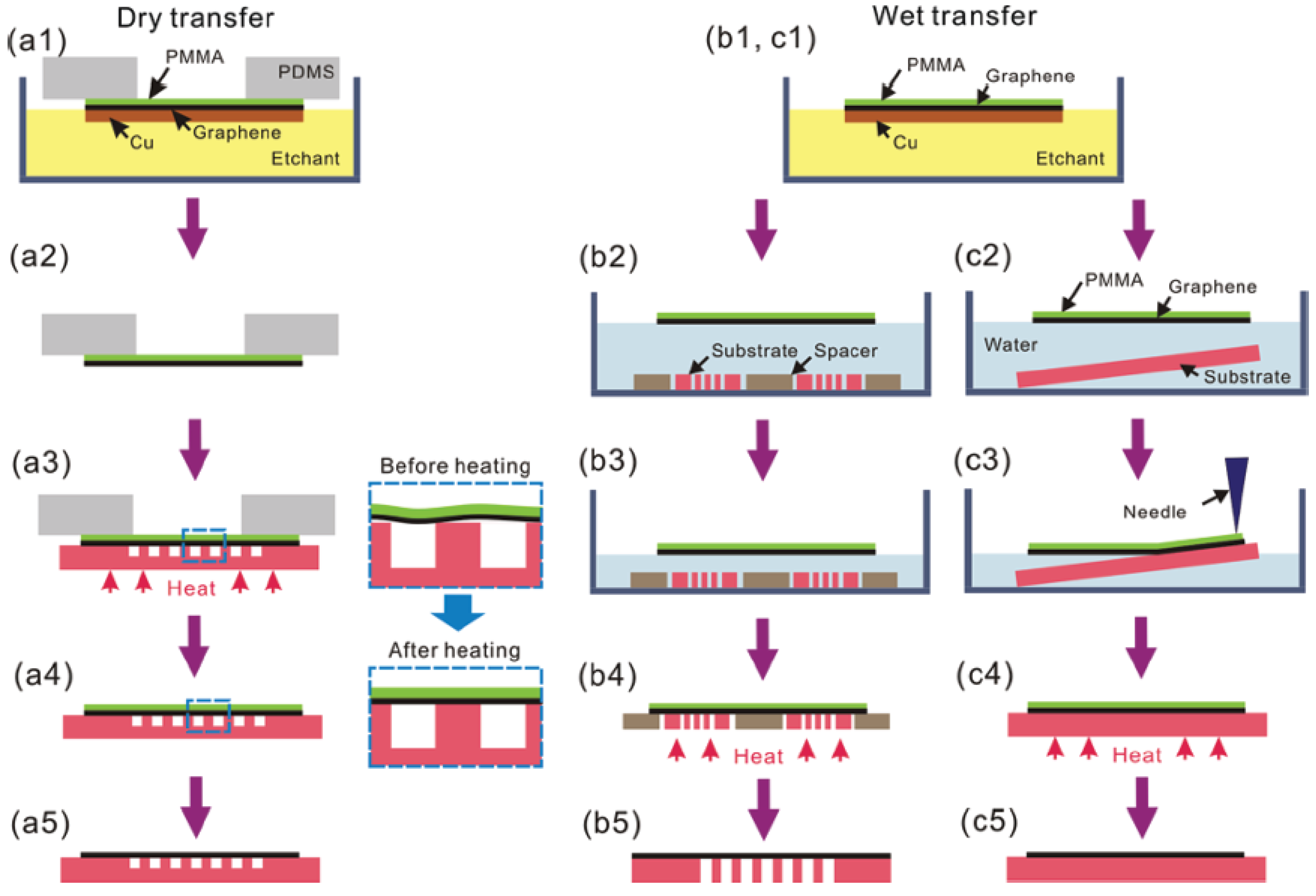
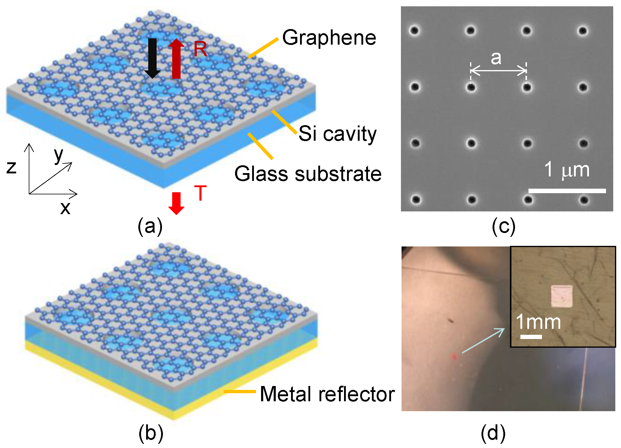
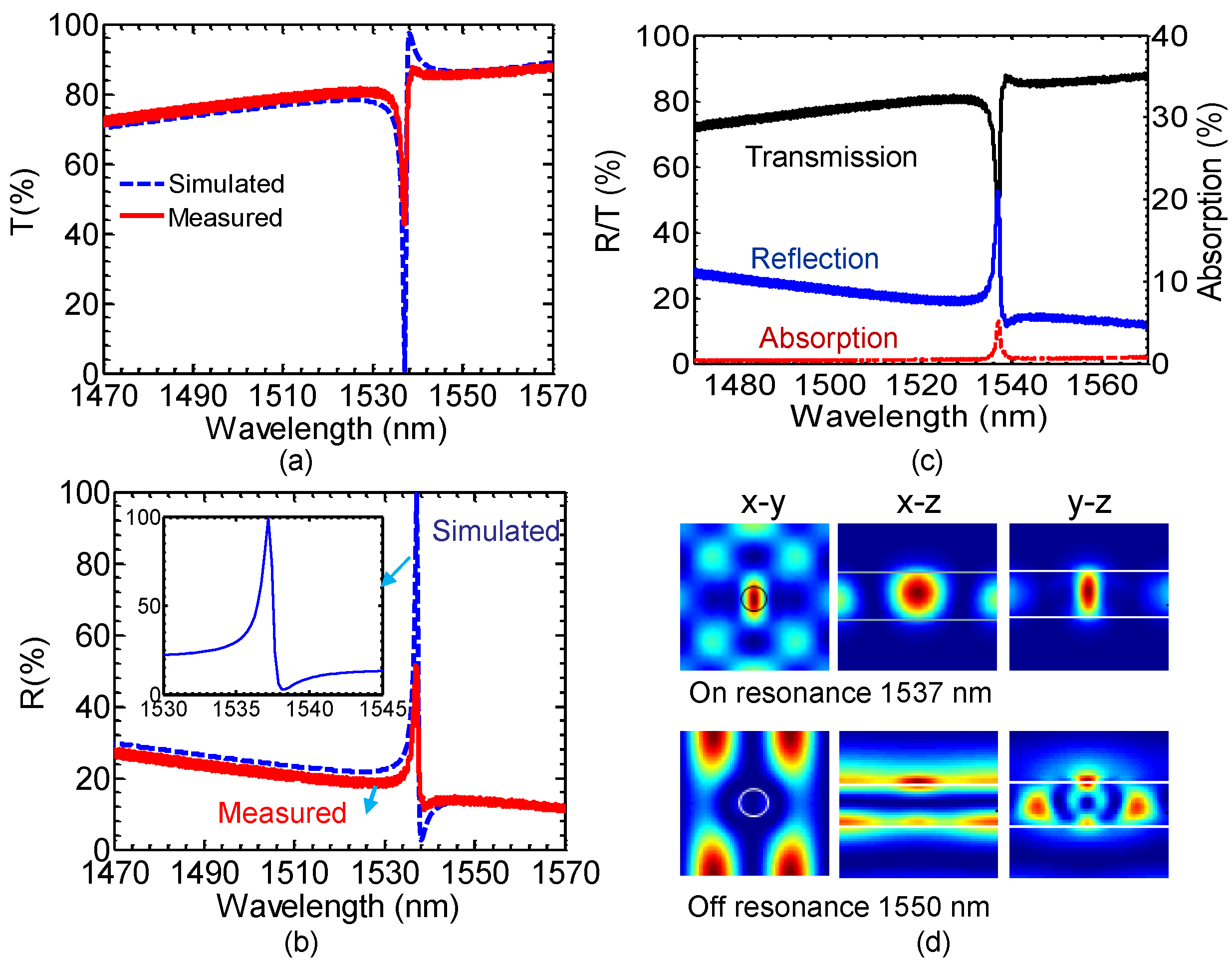
4. Transfer Printing of Graphene Monolayer


5. Summary
Acknowledgments
Conflicts of Interest
References
- Del Alamo, J.A. The high-electron mobility transistor at 30: Impressive accomplishments and exciting prospects. In Presented at the International Conference on Compound Semiconductor Manufacturing Technology (CS MANTECH), Palm Springs, CA, USA, 16–19 May 2011; pp. 17–22.
- Celler, G.K. Fabrication of dielectrically isolated devices utilizing buried oxygen implant and subsequent heat treatment at temperatures above 1300°C. US Patent 4676841 A, 1987. [Google Scholar]
- Rogers, J.A.; Lagally, M.G.; Nuzzo, R.G. Synthesis, assembly and applications of semiconductor nanomembranes. Nature 2011, 477, 45–53. [Google Scholar] [CrossRef] [PubMed]
- Hwang, S.W.; Tao, H.; Kim, D.H.; Cheng, H.; Song, J.K.; Rill, E.; Brenckle, M.A.; Panilaitis, B.; Won, S.M.; Kim, Y.S.; et al. A physically transient form of silicon electronics. Science 2012, 337, 1640–1644. [Google Scholar] [CrossRef] [PubMed]
- Schmidt, O.G.; Eberl, K. Nanotechnology: solid thin solid films roll up into nanotubes. Nature 2001, 410, 168. [Google Scholar] [CrossRef] [PubMed]
- Trotta, R.; Atkinson, P.; Plumhof, J.; Zallo, E.; Rezaev, R.; Kumar, S.; Baunack, S.; Schröter, J.; Rastelli, A.; Schmidt, O. Nanomembrane quantum light emitting diodes integrated onto piezoelectric actuators. Adv. Mater. 2012, 24, 2668–2672. [Google Scholar] [CrossRef] [PubMed]
- Li, X. Self-rolled-up microtube ring resonators: A review of geometrical and resonant properties. Adv. Opt. Photon. 2011, 3, 366–387. [Google Scholar] [CrossRef]
- Scott, S.A.; Lagally, M.G. Elastically strain-sharing nanomembranes: Flexible and transferable strained silicon and silicon-germanium alloys. J. Phys. D Appl. Phys. 2007, 40, R75–R92. [Google Scholar] [CrossRef]
- Yuan, H.C.; Ma, Z.; Roberts, M.M.; Savage, D.E.; Lagally, M.G. High-speed strained-single-crystal-silicon thin-film transistors on flexible polymers. J. Appl. Phys. 2006, 100. [Google Scholar] [CrossRef]
- Sun, L.; Qin, G.; Seo, J.H.; Celler, G.K.; Zhou, W.; Ma, Z. 12 GHz thin film transistors on transferrable silicon nanomembranes for high performance flexible electronics (cover story). Small 2010, 6, 2553–2557. [Google Scholar] [CrossRef] [PubMed]
- Zhang, K.; Seo, J.H.; Zhou, W.; Ma, Z. Fast flexible electronics using transferrable silicon nanomembranes (topical review). J. Phys. D Appl. Phys. 2012, 45. [Google Scholar] [CrossRef]
- Zhou, W.; Ma, Z.; Yang, H.; Qiang, Z.; Qin, G.; Pang, H.; Chen, L.; Yang, W.; Chuwongin, S.; Zhao, D. Flexible photonic-crystal fano filters based on transferred semiconductor nanomembranes. J. Phys. D Appl. Phys. 2009, 42. [Google Scholar] [CrossRef]
- Zhou, W.; Ma, Z.; Yang, H.; Chen, L.; Yang, W.; Qiang, Z.; Qin, G.; Pang, H.; Chuwongin, S.; Zhao, D. Semiconductor nanomembranes for stacked and flexible photonics. In Proceedings of the International Society for Optics and Photonics, San Francisco, CA, USA, 23 January 2010; p. 76060U.
- Yang, H.; Zhao, D.; Chuwongin, S.; Seo, J.H.; Yang, W.; Shuai, Y.; Berggren, J.; Hammar, M.; Ma, Z.; Zhou, W. Transfer-printed stacked nanomembrane lasers on silicon. Nat. Photon. 2012, 6, 615–620. [Google Scholar] [CrossRef]
- Zhou, H.; Seo, J.-H.; Paskiewicz, D.M.; Zhu, Y.; Celler, G.K.; Voyles, P.M.; Zhou, W.; Lagally, M.G.; Ma, Z. Fast flexible electronics with strained silicon nanomembranes. Sci. Rep. 2013, 3. [Google Scholar] [CrossRef] [PubMed]
- Meitl, M.A.; Zhu, Z.T.; Kumar, V.; Lee, K.J.; Feng, X.; Huang, Y.Y.; Adesida, I.; Nuzzo, R.G.; Rogers, J.A. Transfer printing by kinetic control of adhesion to an elastomeric stamp. Nat. Mater. 2006, 5, 33–38. [Google Scholar] [CrossRef]
- Harazim, S.M.; Quinones, V.A.B.; Kiravittaya, S.; Sanchez, S.; Schmidt, O. Lab-in-a-tube: On-chip integration of glass optofluidic ring resonators for label-free sensing applications. Lab Chip 2012, 12, 2649–2655. [Google Scholar] [CrossRef] [PubMed]
- Song, Y.M.; Xie, Y.; Malyarchuk, V.; Xiao, J.; Jung, I.; Choi, K.-J.; Liu, Z.; Park, H.; Lu, C.; Kim, R.-H. Digital cameras with designs inspired by the arthropod eye. Nature 2013, 497, 95–99. [Google Scholar] [CrossRef] [PubMed]
- Zhou, W.; Ma, Z. Breakthroughs in nanomembranes and nanomembrane lasers. IEEE Photon. J. 2013, 5. [Google Scholar] [CrossRef]
- Zhou, W.; Zhao, D.; Shuai, Y.-C.; Yang, H.; Chuwongin, S.; Chadha, A.; Seo, J.-H.; Wang, K.X.; Liu, V.; Ma, Z. Progress in 2D photonic crystal Fano resonance photonics. Prog. Quant. Electron. 2014, 38, 1–74. [Google Scholar] [CrossRef]
- Hu, J.; Li, L.; Lin, H.; Zhang, P.; Zhou, W.; Ma, Z. Flexible integrated photonics: Where materials, mechanics and optics meet (invited). Opt. Mater. Express 2013, 3, 1313–1331. [Google Scholar] [CrossRef]
- Roberts, M.M.; Klein, L.J.; Savage, D.E.; Slinker, K.A.; Friesen, M.; Celler, G.; Eriksson, M.A.; Lagally, M.G. Elastically relaxed free-standing strained-silicon nanomembranes. Nat. Mater. 2006, 5, 388–393. [Google Scholar] [CrossRef] [PubMed]
- Rogers, J.A.; Someya, T.; Huang, Y. Materials and mechanics for stretchable electronics. Science 2010, 327, 1603–1607. [Google Scholar] [CrossRef] [PubMed]
- Janglin, C.; Liu, C.T. Technology advances in flexible displays and substrates. IEEE Access 2013, 1, 150–158. [Google Scholar] [CrossRef]
- Ko, H.; Takei, K.; Kapadia, R.; Chuang, S.; Fang, H.; Leu, P.W.; Ganapathi, K.; Plis, E.; Kim, H.S.; Chen, S.-Y. Ultrathin compound semiconductor on insulator layers for high-performance nanoscale transistors. Nature 2010, 468, 286–289. [Google Scholar] [CrossRef] [PubMed]
- Chen, Y.; Li, H.; Li, M. Flexible and tunable silicon photonic circuits on plastic substrates. Sci. Rep. 2012, 2. [Google Scholar] [CrossRef] [PubMed]
- Seo, J.H.; Zhang, K.; Kim, M.; Zhao, D.; Yang, H.; Zhou, W.; Ma, Z. Flexible phototransistors based on single-crystalline silicon nanomembranes. Adv. Opt. Mater. 2015. [Google Scholar] [CrossRef]
- Seo, J.-H.; Zhang, Y.; Yuan, H.-C.; Wang, Y.; Zhou, W.; Ma, J.; Ma, Z.; Qin, G. Investigation of various mechanical bending strains on characteristics of flexible monocrystalline silicon nanomembrane diodes on a plastic substrate. Microelectron. Eng. 2013, 110, 40–43. [Google Scholar] [CrossRef]
- Gao, L.; Zhang, Y.; Malyarchuk, V.; Jia, L.; Jang, K.-I.; Webb, R.C.; Fu, H.; Shi, Y.; Zhou, G.; Shi, L. Epidermal photonic devices for quantitative imaging of temperature and thermal transport characteristics of the skin. Nat. Commun. 2014, 5. [Google Scholar] [CrossRef] [PubMed]
- Huang, C.C.; Wu, X.; Liu, H.; Aldalali, B.; Rogers, J.A.; Jiang, H. Large-field-of-view wide-spectrum artificial reflecting superposition compound eyes. Small 2014, 10, 3050–3057. [Google Scholar] [CrossRef] [PubMed]
- Xu, X.; Subbaraman, H.; Kwong, D.; Hosseini, A.; Zhang, Y.; Chen, R.T. Large area silicon nanomembrane photonic devices on unconventional substrates. IEEE Photon. Technol. Lett. 2013, 25, 1601–1604. [Google Scholar] [CrossRef]
- Huang, M.C.Y.; Zhou, Y.; Chang-Hasnain, C.J. A surface-emitting laser incorporating a high-index-contrast subwavelength grating. Nat. Photon. 2007, 1, 119–122. [Google Scholar] [CrossRef]
- Magnusson, R.; Shokooh-Saremi, M. Physical basis for wideband resonant reflectors. Opt. Express 2008, 16, 3456–3462. [Google Scholar] [CrossRef] [PubMed]
- Chang-Hasnain, C.J. High-contrast gratings as a new platform for integrated optoelectronics. Semicond. Sci. Technol. 2011, 26. [Google Scholar] [CrossRef]
- Fan, S.; Joannopoulos, J.D. Analysis of guided resonances in photonic crystal slabs. Phys. Rev. B 2002, 65. [Google Scholar] [CrossRef]
- Yang, H.; Chuwongin, S.; Qiang, Z.; Chen, L.; Pang, H.; Ma, Z.; Zhou, W. Resonance control of membrane reflectors with effective index engineering. Appl. Phys. Lett. 2009, 95. [Google Scholar] [CrossRef]
- Yang, H.; Zhao, D.; Seo, J.-H.; Chuwongin, S.; Kim, S.; Rogers, J.A.; Ma, Z.; Zhou, W. Broadband membrane reflectors on glass. IEEE Photon. Technol. Lett. 2012, 24, 476–478. [Google Scholar] [CrossRef]
- Liu, S.-C.; Zhao, D.; Seo, J.-H.; Liu, Y.; Ma, Z.; Zhou, W. Athermal photonic crystal membrane reflectors on diamond. IEEE Photon. Technol. Lett. 2015, 27, 1072–1075. [Google Scholar] [CrossRef]
- Yang, H.; Pang, H.; Qiang, Z.; Ma, Z.; Zhou, W. Surface-normal fano filters based on transferred silicon nanomembranes on glass substrates. Electron. Lett. 2008, 44, 858–859. [Google Scholar] [CrossRef]
- Qiang, Z.; Yang, H.; Chen, L.; Pang, H.; Ma, Z.; Zhou, W. Fano filters based on transferred silicon nanomembranes on plastic substrates. Appl. Phys. Lett. 2008, 93. [Google Scholar] [CrossRef]
- Johnson, S.G.; Fan, S.; Villeneuve, P.R.; Joannopoulos, J.; Kolodziejski, L. Guided modes in photonic crystal slabs. Phys. Rev. B 1999, 60. [Google Scholar] [CrossRef]
- Suh, W.; Solgaard, O.; Fan, S. Displacement sensing using evanescent tunneling between guided resonances in photonic crystal slabs. J. Appl. Phys. 2005, 98. [Google Scholar] [CrossRef]
- Shuai, Y.; Zhao, D.; Singh Chadha, A.; Seo, J.-H.; Yang, H.; Fan, S.; Ma, Z.; Zhou, W. Coupled double-layer fano resonance photonic crystal filters with lattice-displacement. Appl. Phys. Lett. 2013, 103. [Google Scholar] [CrossRef]
- Ma, Z.; Zhou, W. Hybrid vertical cavity light emitting sources. US Patent 20120228582 A1, 2012. [Google Scholar]
- Zhao, D.; Yang, H.; Chuwongin, S.; Seo, J.H.; Ma, Z.; Zhou, W. Design of photonic crystal membrane reflector based vcsels. IEEE Photon. J. 2012, 4, 2169–2175. [Google Scholar] [CrossRef]
- Justice, J.; Bower, C.; Meitl, M.; Mooney, M.B.; Gubbins, M.A.; Corbett, B. Wafer-scale integration of group iii-v lasers on silicon using transfer printing of epitaxial layers. Nat. Photon. 2012, 6, 610–614. [Google Scholar] [CrossRef]
- Yang, W.; Yang, H.; Qin, G.; Ma, Z.; Berggren, J.; Hammar, M.; Soref, R.; Zhou, W. Large-area inp-based crystalline nanomembrane flexible photodetectors. Appl. Phys. Lett. 2010, 96. [Google Scholar] [CrossRef]
- Suk, J.W.; Kitt, A.; Magnuson, C.W.; Hao, Y.; Ahmed, S.; An, J.; Swan, A.K.; Goldberg, B.B.; Ruoff, R.S. Transfer of cvd-grown monolayer graphene onto arbitrary substrates. ACS Nano 2011, 5, 6916–6924. [Google Scholar] [CrossRef] [PubMed]
- Choi, M.K.; Park, I.; Kim, D.C.; Joh, E.; Park, O.K.; Kim, J.; Kim, M.; Choi, C.; Yang, J.; Cho, K.W. Thermally controlled, patterned graphene transfer printing for transparent and wearable electronic/optoelectronic system. Adv. Funct. Mater. 2015. [Google Scholar] [CrossRef]
- Yang, S.Y.; Oh, J.G.; Jung, D.Y.; Choi, H.; Yu, C.H.; Shin, J.; Choi, C.G.; Cho, B.J.; Choi, S.Y. Metal-etching-free direct delamination and transfer of single-layer graphene with a high degree of freedom. Small 2015, 11, 175–181. [Google Scholar] [CrossRef] [PubMed]
- Liu, Y.; Chadha, A.; Zhao, D.; Piper, J.R.; Jia, Y.; Shuai, Y.; Menon, L.; Yang, H.; Ma, Z.; Fan, S. Approaching total absorption at near infrared in a large area monolayer graphene by critical coupling. Appl. Phys. Lett. 2014, 105. [Google Scholar] [CrossRef]
- Piper, J.R.; Fan, S. Total absorption in a graphene monolayer in the optical regime by critical coupling with a photonic crystal guided resonance. ACS Photon. 2014, 1, 347–353. [Google Scholar] [CrossRef]
- Li, X.; Cai, W.; An, J.; Kim, S.; Nah, J.; Yang, D.; Piner, R.; Velamakanni, A.; Jung, I.; Tutuc, E.; et al. Large-area synthesis of high-quality and uniform graphene films on copper foils. Science 2009, 324, 1312–1314. [Google Scholar] [CrossRef] [PubMed]
- Luk’yanchuk, B.; Zheludev, N.I.; Maier, S.A.; Halas, N.J.; Nordlander, P.; Giessen, H.; Chong, C.T. The fano resonance in plasmonic nanostructures and metamaterials. Nat. Mater. 2010, 9, 707–715. [Google Scholar] [CrossRef] [PubMed]
- Choi, M.K.; Yang, J.; Kang, K.; Kim, D.C.; Choi, C.; Park, C.; Kim, S.J.; Chae, S.I.; Kim, T.-H.; Kim, J.H. Wearable red-green-blue quantum dot light-emitting diode array using high-resolution intaglio transfer printing. Nat. Commun. 2015, 6. [Google Scholar] [CrossRef] [PubMed]
- Son, D.; Lee, J.; Qiao, S.; Ghaffari, R.; Kim, J.; Lee, J.E.; Song, C.; Kim, S.J.; Lee, D.J.; Jun, S.W. Multifunctional wearable devices for diagnosis and therapy of movement disorders. Nat. Nanotechnol. 2014, 9, 397–404. [Google Scholar] [CrossRef] [PubMed]
- Kim, J.; Lee, M.; Shim, H.J.; Ghaffari, R.; Cho, H.R.; Son, D.; Jung, Y.H.; Soh, M.; Choi, C.; Jung, S. Stretchable silicon nanoribbon electronics for skin prosthesis. Nat. Commun. 2014, 5. [Google Scholar] [CrossRef] [PubMed]
- Melzer, M.; Karnaushenko, D.; Lin, G.; Baunack, S.; Makarov, D.; Schmidt, O.G. Direct transfer of magnetic sensor devices to elastomeric supports for stretchable electronics. Adv. Mater. 2015, 27, 1333–1338. [Google Scholar] [CrossRef] [PubMed]
© 2015 by the authors; licensee MDPI, Basel, Switzerland. This article is an open access article distributed under the terms and conditions of the Creative Commons Attribution license (http://creativecommons.org/licenses/by/4.0/).
Share and Cite
Yang, H.; Zhao, D.; Liu, S.; Liu, Y.; Seo, J.-H.; Ma, Z.; Zhou, W. Transfer Printed Nanomembranes for Heterogeneously Integrated Membrane Photonics. Photonics 2015, 2, 1081-1100. https://doi.org/10.3390/photonics2041081
Yang H, Zhao D, Liu S, Liu Y, Seo J-H, Ma Z, Zhou W. Transfer Printed Nanomembranes for Heterogeneously Integrated Membrane Photonics. Photonics. 2015; 2(4):1081-1100. https://doi.org/10.3390/photonics2041081
Chicago/Turabian StyleYang, Hongjun, Deyin Zhao, Shihchia Liu, Yonghao Liu, Jung-Hun Seo, Zhenqiang Ma, and Weidong Zhou. 2015. "Transfer Printed Nanomembranes for Heterogeneously Integrated Membrane Photonics" Photonics 2, no. 4: 1081-1100. https://doi.org/10.3390/photonics2041081
APA StyleYang, H., Zhao, D., Liu, S., Liu, Y., Seo, J.-H., Ma, Z., & Zhou, W. (2015). Transfer Printed Nanomembranes for Heterogeneously Integrated Membrane Photonics. Photonics, 2(4), 1081-1100. https://doi.org/10.3390/photonics2041081