Article

Strain-Dependent Dielectric and Optical Properties of Monolayer MoS2 with Phase-Sensitive Surface Plasmon Resonance (SPR) Method

1
School of Physics and Mechanics, Wuhan University of Technology, Wuhan 430070, China
2
Faculty of Science and Engineering, Swansea University, Swansea SA1 8EN, UK
3
Wuhan Yusheng Optoelectronic Co., Ltd., Wuhan 430200, China
*
Authors to whom correspondence should be addressed.
Photonics 2026, 13(6), 523; https://doi.org/10.3390/photonics13060523
Submission received: 21 April 2026 / Revised: 23 May 2026 / Accepted: 26 May 2026 / Published: 28 May 2026
(This article belongs to the Special Issue Advances in Semiconductor Materials)

Abstract

Monolayer molybdenum disulfide (MoS2) holds great promise for strain-tunable optoelectronic devices. The strain-dependent dielectric function is a core parameter to characterize the tunability of optoelectronic properties. However, due to the extremely short light–matter interaction path length for atomically thin materials, measurements are challenging. In this work, we measured the dielectric function of strained monolayer MoS2 using the surface plasmon resonance (SPR) method with the simulated annealing particle swarm optimization (SAPSO) algorithm. When the applied strain ranged from −0.23% (compressive strain) to +0.20% (tensile strain), the dielectric function at seven characteristic wavelengths around the exciton absorption peaks was extracted. Our results demonstrate that both the real part (ε2r) and the imaginary part (ε2i) of the dielectric function evolved almost linearly with the applied strain from −0.23% to +0.20%. Based on these results, we further obtained the strain-induced variations in the refractive index (n) and the extinction coefficient (k). At exciton absorption peak B (600 nm), the strain-induced change rate for n reached a maximum of about −0.0141%−1. At the rising edge of the B exciton absorption (580 nm), the strain-induced change rate for k reached a maximum of about −0.3261%−1. This work presents a quantitative extraction of strain-dependent dielectric function of monolayer MoS2 over excitonic band-edge wavelengths using phase SPR–SAPSO fitting. The proposed method can be extended to the measurement of other atomically thin materials.

1. Introduction

In recent years, monolayer molybdenum disulfide (MoS2) has garnered significant attention in the field of strain-tunable optoelectronic devices [1,2,3] due to its direct bandgap (1.8~1.9 eV) [4,5] and excellent mechanical flexibility [6,7]. The optical properties of strained monolayer MoS2 can be quantitatively characterized by its dielectric function. In prior studies, the strain-dependent dielectric function and optical properties of monolayer MoS2 were usually studied using first-principles simulations [7,8,9,10,11]. However, the simulation results from different computational methods often exhibit some discrepancies [12,13,14,15,16]. The spectroscopic ellipsometry (SE) method is a common technique for measuring the dielectric function spectra of monolayer MoS2 [17,18], but it encounters an inherent difficulty when strain is applied. Due to the atomic thinness of the material, the optical response from the substrate (e.g., SiO2/Si) or metal substrate often overwhelms its intrinsic signal, making it difficult for the SE method to extract the tiny strain-induced changes [19].
To tackle this challenge, we employed the surface plasmon resonance (SPR) method to measure the strain-dependent dielectric function for monolayer MoS2. The SPR method offers extremely high sensitivity for detecting tiny changes in the dielectric function [20,21,22,23,24] and is expected to overcome the difficulty posed by the weak optical response from atomically thin materials [25]. In this work, we systematically measured the dielectric function of monolayer MoS2 at seven characteristic wavelengths (580, 600, 617, 633, 645, 654, and 670 nm) when the strain ranged from −0.23% (compressive strain) to +0.20% (tensile strain). Our results show that the real part (ε2r) of the dielectric function decreased monotonically as the applied strain changed from compressive to tensile while the imaginary part (ε2i) exhibited opposite trends on the two sides of the exciton absorption edge. Further analysis revealed that the strain response of the refractive index was most pronounced at exciton absorption peak B (600 nm), with a change rate of approximately −0.0141%−1. The strongest strain response of the extinction coefficient was at rising edge D (580 nm), where the change rate reached −0.3261%−1 and the corresponding change rate of the absorption coefficient was about −7.0618 × 104 cm−1%−1. The measurement method proposed in this work can be extended to the characterization of the strain-dependent optical properties of other atomically thin materials.

2. Results and Discussion

SPR technology utilizes p-polarized light to excite the evanescent field and surface plasmon polaritons at the metal–dielectric interface. At the resonance angle, the reflected light intensity drops sharply, accompanied by a phase jump. In contrast, the s-polarized light cannot excite the surface plasmons, and its reflection follows the classical Fresnel equations. By measuring the phase difference between the p- and s-polarized reflected light, the common-mode environmental noise can be effectively suppressed, and the phase response caused solely by changes in interfacial dielectric properties is isolated. Prior studies have demonstrated that the phase SPR detection method offers an ultrahigh sensitivity of 10−6 refractive index units (RIUs) [25,26,27].
Figure 1a illustrates the basic structure of our SPR sensing unit. It comprises three parts: a prism (BK7), a sensing layer (MoS2/Au) and a strain-loading holder. Considering that the excellent chemical stability of the Au film and its negligible intrinsic elasto-optic effect [28,29] can effectively eliminate interference from the substrate’s own response during measurements, this experiment utilized the Au film to excite SPR. The Au film was deposited on a BK7 glass substrate by magnetron sputtering. Monolayer MoS2 flakes were synthesized via chemical vapor deposition (CVD) and transferred onto the gold film surface using a wet transfer method. Detailed preparation and transfer procedures are provided in the Methods section. After transfer, the surface morphology of the MoS2 was characterized by atomic force microscopy (AFM) (Figure 1b). The root mean square (RMS) of the topographic image was 0.3 nm. The top view of the strain-loading holder is shown in Figure 1c. Two polydimethylsiloxane (PDMS) blocks were placed in the two small grooves; one groove was fixed, while the other could move horizontally within a sliding track. The two grooves were connected by a pair of small rigid springs. The sliding groove displacement distance, Δx, was controlled via a micrometer to control the applied force (F = −kΔx). After bonding the sensing layer together with the strain-loading holder, precise control of the sliding groove, Δx, allowed for the release or compression of the spring, and then F was transmitted to the monolayer MoS2 through the PDMS. Therefore, the monolayer MoS2 could be modulated by the tensile and the compressive strain.
Figure 1d illustrates the diagram of the measurement system. It employs a broadband laser (SC-PRO, YSL) with a wavelength modulator as the incident light source. The incident beam path is collimated using a pair of mirrors. The beam is shaped by an aperture and then passed through a polarizer to generate a 45° linearly polarized light. The SPR sensing unit is fixed on a high-precision rotation stage (PRM1Z8, Thorlabs). A mirror mounted on the rotation stage is parallel to the bottom surface of the prism within the SPR sensing unit. It was used to convert the rotational movement of the reflected beam’s central position caused by changes in the incident angle into translational motion, facilitating subsequent perpendicular reception by the polarization detector. The polarization detector (PAX10001R1, Thorlabs) was mounted on a three-axis translation stage and continuously acquired the polarization state information at the center of the reflected beam at 0.05 s intervals. The phase difference, Δϕ = ϕpϕs, represents the phase of the p-component relative to the s-component and could be obtained by measuring the Stokes vector, S (S0, S1, S2, and S3), of the reflected light:
S = S 0 S 1 S 2 S 3 = E p 2 + E s 2 E p 2 E s 2 2 E p E s cos ϕ 2 E p E s sin ϕ
where Ep and Es are the electric field of the p-component and the s-component, respectively. Therefore, the phase difference, Δϕ, can be expressed as
Δ ϕ = tan 1 S 3 S 2
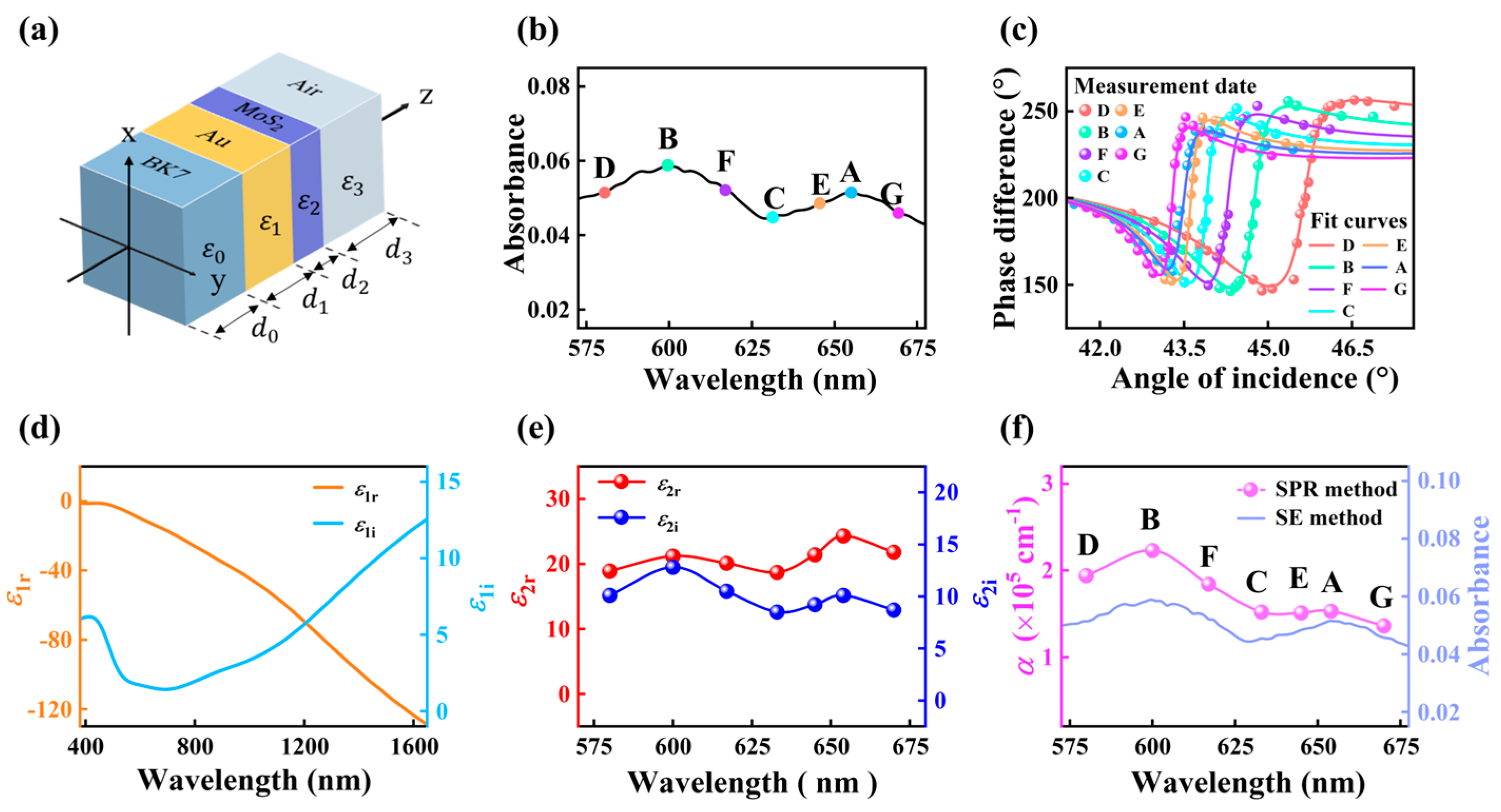
The transfer matrix method (TMM) [30,31,32] was used to analyze the recorded phase signal from the MoS2/Au composite structure. As shown in Figure 2a, the TMM model consists of the prism layer (layer 0), the Au layer (layer 1), the MoS2 layer (layer 2), and the air layer (layer 3). The critical parameters for each layer include the dielectric function, εi (i = 0, 1, 2, 3), and the thickness, di (i = 0, 1, 2, 3). We assumed the incident beam was a monochromatic plane wave, and the electric field transmission in each layer is described by its characteristic matrix, Mi (i = 0, 1, 2, 3):
M i = cos δ i i Q i sin δ i   i Q i sin δ i cos δ i
The total system transfer matrix, Mt, is the product of the individual layer matrices:
M t = M 0 · M 1 · M 2 · M 3 = m 11 m 12 m 21 m 22
The reflection coefficient, r, at the prism–Au film interface was calculated from the elements of the Mt and the boundary conditions:
r = ( m 11 + m 12 Q 3 ) Q 0 ( m 21 + m 22 Q 3 ) ( m 11 + m 12 Q 3 ) Q 0 + ( m 21 + m 22 Q 3 )
The optical admittance, Qi (i = 0, 1, 2, 3), for s-polarized light (Qsi) and p-polarized light (Qpi) could be, respectively, expressed as
Q s i = ε i ε 0 s i n 2 θ 0
Q p i = ε i ε i ε 0 s i n 2 θ 0
The phase factor, δi, could be expressed using εi and di:
δ i = 2 π λ · d i · ε i ε 0 s i n 2 θ 0
where θ0 and λ are the incident angle in the prism and the incident wavelength. The phase shift was derived from the argument of the r. Therefore, the phase difference, Δϕ, could be extracted by
ϕ = arg r p arg r s
To ensure that the evanescent field possessed sufficient penetration depth and localized electric field intensity to effectively probe the phase difference from the monolayer MoS2, the thickness of the Au substrate was selected to be about 45 nm (typically, an Au film thickness of 45~50 nm yields the strongest localized electric field for SPR excitation [33]). In this experiment, the thickness of the Au substrate (45 nm) and monolayer MoS2 (0.7 nm) were confirmed using a stylus profiler and AFM, as detailed in the Supporting Information, part 1. The exciton A and B absorption spectra of the monolayer MoS2 over the wavelength range of 560 nm to 680 nm were acquired by the transmission-mode SE method using a differential measurement scheme. By measuring the transmitted light intensity ratio between the samples with and without the MoS2 layer, the contribution from the Au substrate was effectively subtracted, allowing the intrinsic absorption spectrum of the MoS2 to be extracted, as shown in Figure 2b. Based on the exciton absorption spectrum, seven characteristic wavelengths—exciton peak A (654 nm), exciton peak B (600 nm), absorption valley C (633 nm), rising edges D and E (580 nm and 645 nm), and falling edges F and G (617 nm and 670 nm)—were selected for subsequent dielectric function measurements. The measurement results of the SPR phase difference as a function of angle at seven characteristic wavelengths are plotted as dots in Figure 2c. In addition, the dielectric function (ε1 = ε1r + iε1i) of the Au substrate was measured by the reflection-mode SE method, as shown in Figure 2d, where the dielectric function spectrum is derived from the polarization state of the light reflected from the gold film surface. With the known dielectric function spectrum and thickness of the Au substrate, as well as the thickness of the monolayer MoS2, the dielectric function (ε2 = ε2r + 2i) of the MoS2 was extracted using the simulated annealing particle swarm optimization (SAPSO) algorithm [34,35]. The flowchart of the SAPSO algorithm is provided in the Supporting Information, part 2. Obviously, in Figure 2c, there is excellent agreement between the fit curve and the measurement data; the mean squared error (MSE) of the fit is less than 0.01. Therefore, the dielectric function of the monolayer MoS2 at seven characteristic wavelengths was extracted, as shown in Figure 2e. The dielectric function extracted by our SPR–SAPSO method is in good agreement with the results reported in the literature, as detailed in the Supporting Information, part 3. Furthermore, the absorption coefficient, α, was derived from the measured dielectric function in Figure 2e. The absorption coefficient spectrum obtained by the SPR method follows the same trend as the absorbance using the transmission-mode SE method, as shown in Figure 2f.
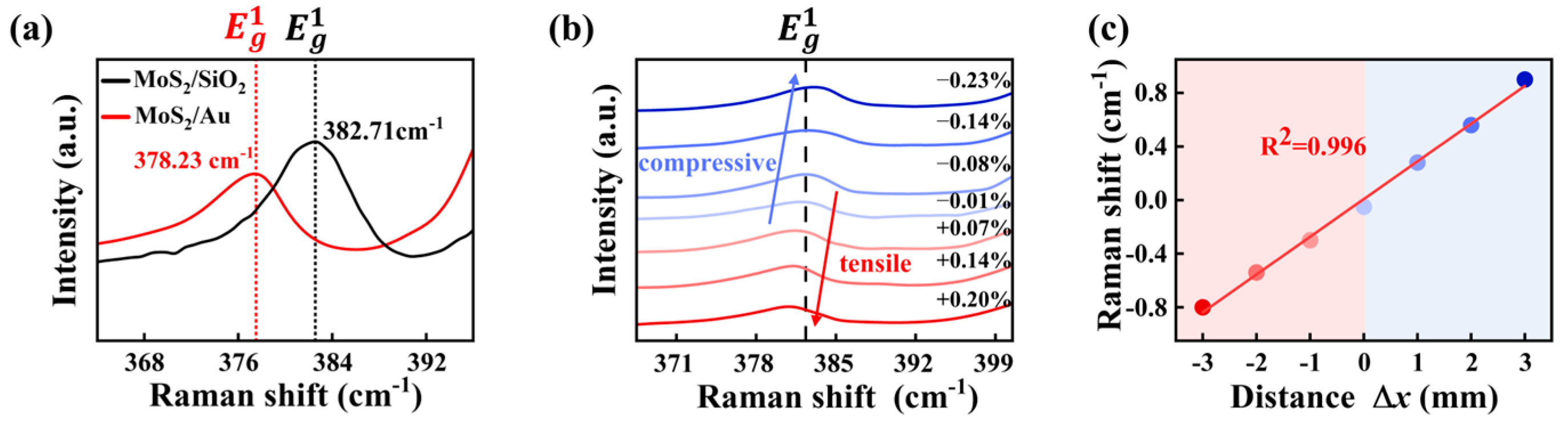
During the monolayer MoS2 flake transfer process, the lattice mismatch between the monolayer MoS2 flake and the Au substrate introduced pre-strain. Therefore, Raman spectroscopy was used to quantitatively evaluate this pre-strain. In this Raman-based strain calibration, we implicitly assumed that the applied deformation was purely in-plane. For the monolayer MoS2, the frequency (ω) of the in-plane vibrational mode ( E g 1 mode) was highly sensitive to the in-plane strain while the out-of-plane vibrational mode (A1g mode) primarily reflected the interlayer coupling information. Consequently, in this experiment, the shift of the E g 1 peak was used to calibrate the value of the strain in the monolayer MoS2. The E g 1 peak position of the original MoS2 flake on the SiO2/Si substrate served as the strain-free reference. According to prior studies [36,37], the strain sensitivity of the E g 1 peak frequency was approximately −4 cm−1%−1. Therefore, the strain (σ) could be calibrated using σ (%) = −Δω/4, where Δω represents the measured peak shift of the E g 1 peak. Obviously, the redshift (negative Δω) of the E g 1 peak corresponded to the tensile strain, while the blueshift (positive Δω) corresponded to the compressive strain. The Raman spectrum of the transferred monolayer MoS2 sample on the 45 nm-thick Au substrate is shown in Figure 3a. Clearly, the E g 1 peak exhibits a redshift of 4.48 cm−1, which indicates that the pre-strain is a tensile strain with a magnitude of 1.12%.
We used the strain-loading holder to compensate for the transfer-induced pre-strain. Figure 3b shows the Raman spectra of the monolayer MoS2 acquired during the linear modulation after the pre-strain was eliminated. It is evident that the E g 1 peak of the monolayer MoS2 transitions from the redshift to the blueshift in response to the applied strain. Based on the shift of the E g 1 peak, we achieved the maximum range of linearly modulated strain of approximately ±0.20% on the monolayer MoS2 sample. Beyond this range, the strain no longer varied linearly with the sliding distance, Δx, of the groove, as detailed in the Supporting Information, part 4. We also characterized the strain uniformity across the monolayer MoS2, as detailed in the Supporting Information, part 5. Figure 3c presents the linear fitting between the E g 1 peak shift and the groove displacement distance, Δx. The shift coefficient of the E g 1 peak is about 0.28 cm−1mm−1. The zero point in the figure corresponds to the state where the pre-strain has been eliminated. The positive and negative values of Δx represent the compressive and tensile strain stages, respectively.
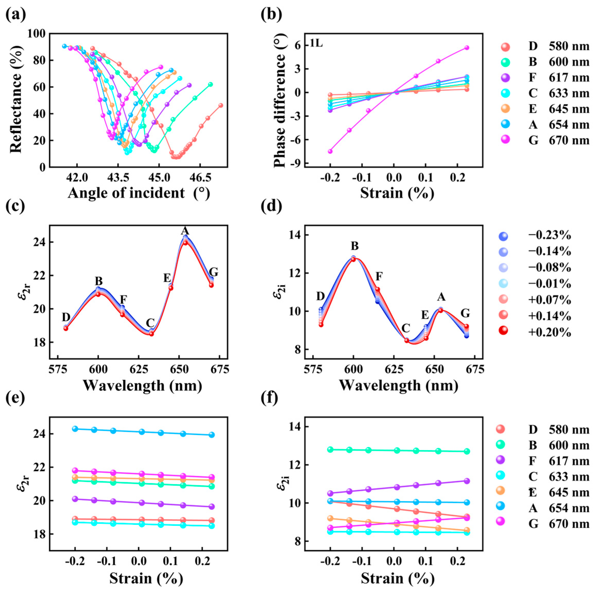
Leveraging the steep slope of the phase difference–angle curve at the resonance angle, the dielectric variation could be converted into a significant phase-difference change. In Figure 4a, the resonance angles at seven characteristic wavelengths were determined by measuring the SPR reflectivity versus the incident angle curves of the MoS2/Au composite structure. When the strain ranged from −0.23% to +0.20%, the relative phase difference variations at the resonance angles for these seven wavelengths were measured (Figure 4b). We clarified the sample-to-sample reproducibility by including data from multiple independent samples, as detailed in the Supporting Information, part 6. Using the SAPSO algorithm, the strain-induced changes in the real part (ε2r) and imaginary part (ε2i) of the dielectric function were extracted, as shown in Figure 4c,d, respectively. A clear strain response of the dielectric function was observed at seven characteristic wavelengths. Obviously, ε2r decreased monotonically as the applied strain changed from compressive to tensile, while ε2i exhibited opposite trends on the two sides of the absorption edge. The results demonstrate that both ε2r and ε2i evolved almost linearly with the applied strain from −0.23% to +0.20%, as shown in Figure 4e,f; Δε2r and Δε2i denote the changes in the real and imaginary parts of the dielectric function relative to the strain-free state. Table 1 presents the change rate of dielectric function per 1% applied strain (σ), obtained by linear fitting as the slope of the variation with strain. At exciton absorption peaks A (654 nm) and B (600 nm) and at absorption valley C (633 nm), the strain-induced change in the dielectric function is dominated by the strain response of ε2r, while the response of ε2i is weak. At rising edges D (580 nm) and E (645 nm) and falling edges F (617 nm) and G (670 nm) of the exciton absorption spectrum, the strain response of ε2i is significantly enhanced. The strain response of ε2r is most pronounced at falling edge F, with a change rate of about −1.071%−1. The strain response of ε2i is most pronounced at rising edge D, with a change rate of about −1.998%−1.
From the extracted dielectric function, the refractive index, n; the extinction coefficient, k; and the absorption coefficient, α, of the monolayer MoS2 could be obtained:
n = ε 2 r 2 + ε 2 i 2 + ε 2 r 2
k = ε 2 r 2 + ε 2 i 2 ε 2 r 2
α = 4 π λ k
The change rates of the refractive index (Δn), the extinction coefficient (Δk), and the absorption coefficient (Δα) per 1% applied strain for monolayer MoS2 are shown in Table 2. Obviously, the strain response of n is the most pronounced at exciton absorption peak B (600 nm), reaching a change rate of −0.0141%−1. The strain response of k is the most pronounced at rising edge D (580 nm) of the exciton absorption spectrum, where the change rate reaches −0.3261%−1, and the corresponding change rate for α is about −7.0618 × 104 cm−1%−1.
To understand the mechanism of the variation in the dielectric and optical properties of monolayer MoS2 under strain, we took a closer look at the strain-induced energy band shift in our prior reported DFT work [11]. At zero strain, monolayer MoS2 is a direct bandgap semiconductor. Upon applying the compressive or tensile strain, the conduction band minimum decreased while the valence band maximum increased, and then this led to the bandgap narrowing. Consequently, the peaks of ε2r and ε2i are red-shifted. The changes for the dielectric function of monolayer MoS2 can be attributed to the modification of the band structure under these strains, which is closely related to the inter-band optical transition probability and the joint density of states. Specifically, ε2i directly corresponds to the allowed inter-band optical transition probability in the Brillouin zone. The magnitude of ε2i is proportional to the joint density of states JDOS [38]:
ε 2 i ω 1 ω 2 · J D O S E
J D O S E = 2 d 3 k 2 π 3 δ E C k E V k E k
where ω, k, δ, E(k), EC(k) and EV(k) are the angular frequencies of the incident light, the wave vector, the Dirac delta function, the photon energy, and the energies of the conduction band and the valence band at wave vector k, respectively. Treating strain as a perturbation to the band structure, the strain-induced change in ε2i at a fixed photon energy can be expressed as
d ε 2 i d σ d J D O S d E · d E C k E V k d σ
The excitonic effect leads to spin-orbit splitting of the valence band and then induces two absorption peaks at the 600 and 654 nm wavelengths, respectively [39]. Strain would alter the lattice constant of the monolayer MoS2 and then shift the resonance frequency of exciton. The redshift and blueshift of the resonance frequency would occur under the tensile and compressive strains, respectively. Then, the shift of the resonance frequency of the excitons leads to a linear response of dielectric function at the absorption edges [40]. Strain modulates the bandgap by altering the lattice constant, causing an overall shift in the bands. However, since ∂JDOS/∂E ≈ 0, the contribution of strain-induced band changes to ε2i comes only from second-order terms, making ε2i insensitive to strain. At absorption valley C (633 nm), JDOS is at a local minimum and varies slowly with energy. Strain-induced band shifts also fail to cause significant changes in ε2i. At rising and falling edges D (580 nm), E (645 nm), F (617 nm) and G (670 nm), these positions lie near the band edges or thresholds of the band structure, where JDOS varies rapidly with energy. When strain induces an overall band shift, ε2i changes significantly. Specifically, at the rising edges, JDOS decreases with the strain changes from compressive to tensile. Therefore, ε2i decreases with strain. On the contrary, at the falling edges, JDOS increases with the strain changes from compressive to tensile. Therefore, ε2i increases with strain. The sensitivity of ε2i to strain is proportional to ∂JDOS/∂E. Therefore, the strain response of ε2i is most pronounced at the band edges.
The development of ε2r is related to ε2i over the entire energy range via the Kramers–Kronig (K–K) relation:
ε 2 r ω = 1 + 2 π P 0 ω 1 ε 2 i ω 1 ω 1 2 ω 2 d ω 1
where P denotes the Cauchy principal value. At exciton absorption peaks A and B and absorption valley C, ε2i is insensitive to strain. Here, the strain response of ε2r mainly originates from the strain-induced overall band shift. This is because the strain changes the lattice structure and thereby induces a shift in the bandgap. As a result, from compressive to tensile strain, ε2r decreases monotonically. At the rising and falling edges, ε2i varies rapidly with energy. The strain response of ε2r is governed by the combined action from the shift in bandgap and the drastic change for ε2i. At the rising edge, ε2i decreases with tensile strain, and this contribution tends to further reduce ε2r. At the falling edge, ε2i increases with tensile strain, which additionally increases ε2r. These strain coefficients suggest that even modest mechanical deformations can produce measurable optical responses in practical devices. For example, a typical operational strain of 0.1~0.2% would already yield a finite modulation of the refractive index and extinction coefficient, which translates into detectable changes in transmission, reflection, or phase in integrated MoS2-based waveguides and cavities. Such a strain-tunable optical response indicates that the proposed platform is promising for compact, flexible strain sensors and mechanically reconfigurable filters or modulators in next-generation photonic circuits.
There are three main potential sources of error in the SPR–SAPSO method. (1) The angular positioning error of the rotation stage is a key factor leading to measurement errors in the resonance angle of the SPR signal. In our experiment, the accuracy of the rotation stage (PRM1Z8, Thorlabs) was approximately 0.005°, which could have led to an uncertainty of about ±0.2 for the ε2r and ε2i. (2) The SPR signal is also sensitive to the output wavelength and power of the laser (SC-PRO, YSL). Although a controller was used to maintain the working temperature and driving current, the output of the laser still slightly fluctuated with time and then induced a phase-difference variation of about 0.2°. After real-time processing through a low-pass filter, averaging 100 data sets acquired over a 5 s period could control the phase fluctuation to 0.01°. This residual phase uncertainty would lead to an uncertainty of about ±0.05 for ε2r and ε2i. (3) The roughness of the monolayer MoS2 and Au substrate would induce the errors for thickness measurement. The surface roughness values of the monolayer MoS2 and Au substrate were approximately 0.3 nm and 0.5 nm, as detailed in the Supporting Information, part 7, which could have induced an uncertainty of about ±0.3 for ε2r and ε2i. Based on the above discussion, the total uncertainty for ε2r and ε2i is about ±0.55.

3. Conclusions

In this work, the dielectric function of monolayer MoS2 was systematically measured using the SPR method when the strain ranged from −0.23% to +0.20% at seven characteristic wavelengths (580–670 nm) in the exciton absorption spectrum. Our results show that ε2r decreased monotonically as the applied strain changed from compressive to tensile, while ε2i exhibited opposite trends on the two sides of the absorption edge. Moreover, both ε2r and ε2i evolved almost linearly with the strain. Based on the measured dielectric function, the strain responses of n, k, and α were further obtained. The strain-induced change rate of n reached a maximum of approximately −0.0141%−1 at exciton absorption peak B (600 nm). The change rate of k was most pronounced at the rising edge of the absorption spectrum (580 nm), reaching −0.3261%−1, with the corresponding change rate of α at about −7.0618 × 104 cm−1%−1. The dielectric measurement method employed in this study is universal and can be readily extended to the measurement of the strain-induced optical properties of other atomically thin materials.

4. Method

Au substrate deposition method: The Au film was deposited by the direct-current magnetron sputtering method. The Au target (99.999%) served as the source material. Prior to deposition, the chamber was evacuated to a base pressure lower than 3 × 10⁻⁴ Pa. High-purity argon gas was then introduced as the working gas, maintaining a process pressure of approximately 2 Pa. A direct current of 20 mA was applied to initiate and sustain the plasma for sputtering.
Growth method for monolayer MoS2 flake: Molybdenum trioxide (MoO3, 99.999% purity) was used as the molybdenum source, and solid sulfur (99.999% purity) was used as the sulfur source, with argon serving as the carrier gas. Growth was carried out in a dual-zone tube furnace with an 80 mm tube diameter. The MoO3 was heated to 650 °C and the sulfur to 180 °C. The growth was conducted at a pressure of 4000 Pa for 10 min on a SiO2/Si substrate.
Transfer method for monolayer MoS2 flake: First, a 4% poly(methyl methacrylate) (PMMA) in anisole solution was drop-cast onto the SiO2/Si substrate with as-grown MoS2 and cured on a hotplate at 100 °C to form a thick supporting film, which facilitated subsequent handling. Next, the sample was immersed in a 2 mol/L KOH solution for approximately 2 h to safely separate the PMMA film from the substrate. The freed PMMA/MoS2 film was then lifted with tweezers, rinsed 3–5 times in deionized water to remove residual KOH, and subsequently scooped up from below using the target substrate (the Au film) to bring the MoS2 into contact. Following transfer, the substrate with the film was placed vertically to air-dry and then annealed on an 80 °C hotplate to improve adhesion. Finally, the PMMA support layer was removed by immersing the sample in acetone. The acetone was replaced 3–5 times, with each soak lasting about 30 min, to ensure complete dissolution of the PMMA. The PMMA support layer was removed repeatedly with acetone to ensure complete dissolution of the PMMA as much as possible.

Supplementary Materials

The following supporting information can be downloaded at: https://www.mdpi.com/article/10.3390/photonics13060523/s1, Figure S1. (a) The thickness measurement for Au substrate using the stylus profiler. (b) The thickness measurement for monolayer MoS2 sample using AFM. Figure S2. Flowchart of the SAPSO algorithm [34,35]. Figure S3. (a) The E g 1 peak versus the applied strain from compressive to tensile strain. (b) The shift of E g 1 peak versus the micrometer displacement distance Δx. Figure S4. (a) Schematic of Raman spectrum characterization. (b) Raman peak shift versus the micrometer displacement distance Δx at three different points. Figure S5. SPR phase difference-strain curves for different wavelengths. (a) 600 and 654 nm. (b) 633 nm. (c) 580 and 645 nm. (d) 617 and 670 nm. Figure S6. (a,b) Topographic images of monolayer MoS2 and Au substrate surfaces, respectively. Table S1. Dielectric function of monolayer MoS2 at the A and B exciton peaks [41,42].

Author Contributions

X.Z., Z.M. and S.D. designed the experiments. X.Z. and H.L. contributed to sample preparation. X.Z., M.L. and S.D. performed the experiments. X.Z., H.L., X.W., L.L. and S.D. contributed to data analysis. X.Z., Z.M., S.D., L.L. and M.L. wrote the paper. All authors have read and agreed to the published version of the manuscript.

Funding

National Natural Science Foundation of China (62304161, 12574515); Key R&D Program of Hubei Province (2024BAB009).

Data Availability Statement

Data underlying the results presented in this paper are not publicly available at this time but may be obtained from the authors upon reasonable request.

Conflicts of Interest

Authors Zhiwen Ming and Shuo Deng were employed by the company Wuhan Yusheng Optoelectronic Co., Ltd. The remaining authors declare that this research was conducted in the absence of any commercial or financial relationships that could be construed as potential conflicts of interest.

References

  1. Du, J.; Yu, H.; Liu, B.; Hong, M.; Liao, Q.; Zhang, Y. Strain engineering in 2D material-based flexible optoelectronics. Small Methods 2021, 5, 2000919. [Google Scholar] [CrossRef]
  2. Yang, K.; Lee, Y.; Rhee, D.; Choi, B.; Alfieri, A. Geometrically confined strain engineering of MoS2 via quasi-van der Waals recrystallization of gold nanopillars. Adv. Sci. 2025, 12, e06488. [Google Scholar] [CrossRef]
  3. Kotbi, A.; Benyoussef, M.; Ressami, E. Gas sensors based on exfoliated g-C3N4 for CO2 detection. Chemosensors 2022, 10, 470. [Google Scholar] [CrossRef]
  4. Mukherjee, S.; Maiti, R.; Midya, A.; Das, S. Tunable direct bandgap optical transitions in MoS2 nanocrystals for photonic devices. ACS Photonics 2015, 2, 760–768. [Google Scholar] [CrossRef]
  5. Tong, X.; Ashalley, E.; Lin, F. Advances in MoS2-based field effect transistors (FETs). Nano-Micro Lett. 2015, 7, 203–218. [Google Scholar] [CrossRef] [PubMed]
  6. Singh, E.; Singh, P.; Kim, K. Flexible molybdenum disulfide (MoS2) atomic layers for wearable electronics and optoelectronics. ACS Appl. Mater. Interfaces 2019, 11, 11061–11105. [Google Scholar] [CrossRef]
  7. Radatovic, B.; Çakıroğlu, O.; Jadrisko, V. Strain-enhanced large-area monolayer MoS2 photodetectors. ACS Appl. Mater. Interfaces 2024, 16, 15596–15604. [Google Scholar] [CrossRef]
  8. Yamusa, S.; Shaari, A.; Alsaif, N. Elucidating the structural, electronic, elastic, and optical properties of bulk and monolayer MoS2 transition-metal dichalcogenides: A DFT approach. ACS Omega 2022, 7, 45719–45731. [Google Scholar] [CrossRef]
  9. Khan, M.; Tripathi, M.; Tripathi, A. Strain-induced structural, elastic, and electronic properties of 1L-MoS2. J. Mater. Res. 2022, 37, 3340–3351. [Google Scholar] [CrossRef]
  10. Deng, S.; Zhang, Y.; Li, L. Strain magnitude and direction effect on the energy band structure of Hexagonal and orthorhombic monolayer MoS2. IEEE Trans. Nanotechnol. 2018, 17, 419–423. [Google Scholar] [CrossRef]
  11. Deng, S.; Li, L.; Li, M. Stability of direct band gap under mechanical strains for monolayer MoS2, MoSe2, WS2 and WSe2. Phys. E Low Dimens. Syst. Nanostruct. 2018, 101, 44–49. [Google Scholar] [CrossRef]
  12. Peng, Q.; De, S. Outstanding mechanical properties of monolayer MoS2 and its application in elastic energy storage. Phys. Chem. Chem. Phys. 2013, 15, 19427–19437. [Google Scholar] [CrossRef]
  13. Johari, P.; Shenoy, V. Tuning the electronic properties of semiconducting transition metal dichalcogenides by applying mechanical strains. ACS Nano 2012, 6, 5449–5456. [Google Scholar] [CrossRef] [PubMed]
  14. Li, Y.; Chernikov, A.; Zhang, X.; Rigosi, A. Measurement of the optical dielectric function of monolayer transition-metal dichalcogenides: MoS2, MoSe2, WS2, and WSe2. Phys. Rev. B 2014, 90, 205422. [Google Scholar] [CrossRef]
  15. Chen, J.; Liu, M.; Liu, M. Accelerating discovery of next-generation power electronics materials via high-throughput ab initio screening. npj Comput. Mater. 2025, 11, 249. [Google Scholar] [CrossRef]
  16. Alqaydi, M.; Kotbi, A.; Rajput, N. Gas sensing capabilities of MoS2 and WS2: Theoretical and experimental study. Emerg. Mater. 2025, 8, 5799–5811. [Google Scholar] [CrossRef]
  17. Nguyen, H.; Nguyen, X.; Hoang, A.; Kim, T. Spectroscopic ellipsometry study of the temperature dependences of the optical and exciton properties of MoS2 and WS2 monolayers. Materials 2024, 17, 5455. [Google Scholar] [CrossRef]
  18. Yoo, S.; Park, Q. Spectroscopic ellipsometry for low-dimensional materials and heterostructures. Nanophotonics 2022, 11, 2811–2825. [Google Scholar] [CrossRef]
  19. Puri, S.; Patel, S.; Cabellos, J.; Rosas-Hernandez, L.; Reynolds, K.; Churchill, H. Substrate interference and strain in the second-harmonic generation from MoSe2 monolayers. Nano Lett. 2024, 24, 13061–13067. [Google Scholar] [CrossRef]
  20. Ahamed, S.; Venkatesan, K.; Jalaludeen, S. A review on various surface plasmon resonance-based sensors. Plasmonics 2025, 20, 6869–6885. [Google Scholar] [CrossRef]
  21. Tao, L.; Deng, S.; Gao, H. Experimental investigation of the dielectric functions of thin noble metallic films using a surface plasmon resonance sensor. Sensors 2020, 20, 1505. [Google Scholar] [CrossRef] [PubMed]
  22. Das, C.; Yang, F.; Yang, Z. Computational modeling for intelligent surface plasmon resonance sensor design and experimental schemes for real-time plasmonic biosensing: A review. Adv. Theory Simul. 2023, 6, 2200886. [Google Scholar] [CrossRef]
  23. Xia, S.; Zhang, D.; Zhai, X. Phase-controlled topological plasmons in 1D graphene nanoribbon array. Appl. Phys. Lett. 2023, 123, 101102. [Google Scholar] [CrossRef]
  24. Mouloua, D.; Kotbi, A.; Deokar, G. Recent progress in the synthesis of MoS2 thin films for sensing, photovoltaic and plasmonic applications: A review. Materials 2021, 14, 3283. [Google Scholar] [CrossRef]
  25. Dai, X.; Meng, C.; Huang, S. Attomolar nucleic acid detection using CRISPR enhanced phase-sensitive surface plasmon resonance imaging. Anal. Chem. 2025, 97, 16296–16303. [Google Scholar] [CrossRef] [PubMed]
  26. Wu, C.; Pao, M. Sensitivity-tunable optical sensors based on surface plasmon resonance and phase detection. Opt. Express 2004, 12, 3509–3514. [Google Scholar] [CrossRef]
  27. Qing, G.; Huang, J.; Zhang, D. All-order dark mode plasmon-induced transparency underpinned by transitional resonance phase. Phys. Rev. B 2026, 113, 125413. [Google Scholar] [CrossRef]
  28. Bassoli, L.; Nizzoli, F.; Sandercock, J. Surface brillouin scattering in polycrystalline gold. Phys. Rev. B 1986, 34, 1296. [Google Scholar] [CrossRef]
  29. Correa-Duarte, M.; Salgueiriño-Maceira, V.; Rinaldi, A. Optical strain detectors based on gold/elastomer nanoparticulated films. Gold Bull. 2007, 40, 6–14. [Google Scholar] [CrossRef]
  30. Ouyang, Q.; Zeng, S.; Jiang, L. Sensitivity enhancement of transition metal dichalcogenides/silicon nanostructure-based surface plasmon resonance biosensor. Sci. Rep. 2016, 6, 28190. [Google Scholar] [CrossRef]
  31. Panda, A.; Pukhrambam, P. Modeling of high-performance SPR refractive index sensor employing novel 2D materials for detection of malaria pathogen. IEEE Trans. Nanobiosci. 2021, 21, 312–319. [Google Scholar] [CrossRef]
  32. Cai, H.; Wang, M.; Wu, Z. Performance enhancement of SPR biosensor using graphene–MoS2 hybrid structure. Nanomaterials 2022, 12, 2219. [Google Scholar] [CrossRef] [PubMed]
  33. Shwan, Y.; Ghafoor, B.; Hamasalih, G. Optimization of surface plasmon resonance (SPR) for gold/air interface by using Kretschmann configuration. Eng. Technol. J. 2022, 40, 1334–1341. [Google Scholar] [CrossRef]
  34. Yue, C.; Qin, Z.; Lang, Y.; Liu, Q. Determination of thin metal film’s thickness and optical constants based on SPR phase detection by simulated annealing particle swarm optimization. Opt. Commun. 2019, 430, 238–245. [Google Scholar] [CrossRef]
  35. Han, L.; Xu, C.; Huang, T.; Dang, X. Improved particle swarm optimization algorithm for high performance SPR sensor design. Appl. Opt. 2021, 60, 1753–1760. [Google Scholar] [CrossRef] [PubMed]
  36. Rice, C.; Young, R.J.; Zan, R.; Bangert, U.; Wolverson, D. Raman-scattering measurements and first-principles calculations of strain-induced phonon shifts in monolayer MoS2. Phys. Rev. B 2013, 87, 081307. [Google Scholar] [CrossRef]
  37. Michail, A.; Anestopoulos, D.; Delikoukos, N. Biaxial strain engineering of CVD and exfoliated single- and bi-layer MoS2 crystals. 2D Mater. 2021, 8, 015023. [Google Scholar] [CrossRef]
  38. Kittel, C.; McEuen, P. Introduction to Solid State Physics; John Wiley & Sons: Hoboken, NJ, USA, 2018. [Google Scholar]
  39. Shi, H.; Pan, H.; Zhang, Y. Quasiparticle band structures and optical properties of strained monolayer MoS2 and WS2. Phys. Rev. B 2013, 87, 155304. [Google Scholar] [CrossRef]
  40. Nayeri, M.; Fathipour, M.; Yazdanpanah, G. Behavior of the dielectric function of monolayer MoS2 under Uniaxial Strain. J. Comput. Electron. 2016, 15, 1388–1392. [Google Scholar] [CrossRef]
  41. Hsu, C.; Frisenda, R.; Schmidt, R. Thickness-dependent refractive index of 1L, 2L, and 3L MoS2, MoSe2, WS2, and WSe2. Adv. Opt. Mater. 2019, 7, 1900239. [Google Scholar] [CrossRef]
  42. Song, B.; Gu, H.; Fang, M. Layer-dependent dielectric function of wafer-scale 2D MoS2. Adv. Opt. Mater. 2019, 7, 1801250. [Google Scholar] [CrossRef]
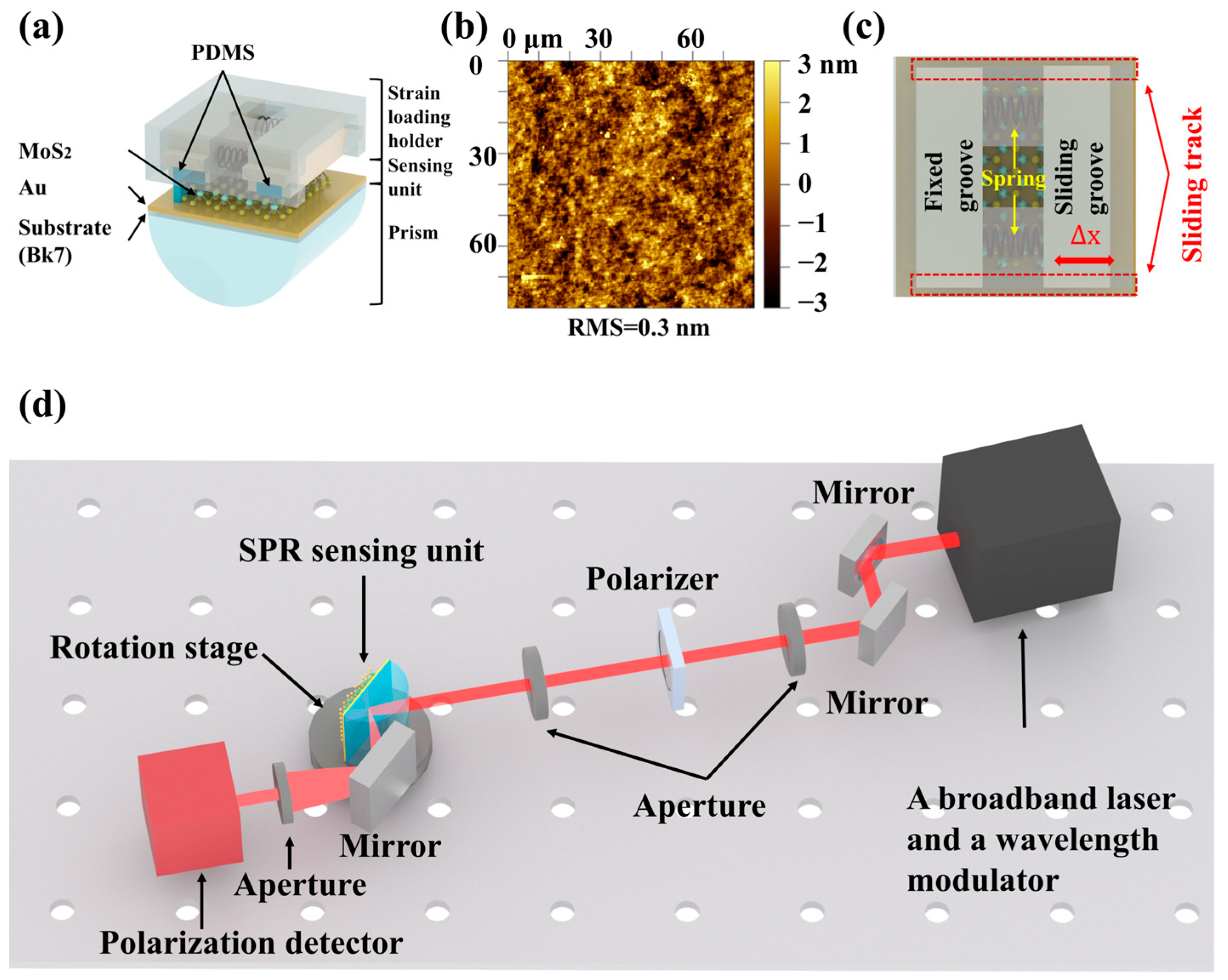
Figure 1. Dielectric function measurement system. (a) The basic structure of the SPR sensing unit. (b) The topographic image of the monolayer MoS2 on the gold substrate. (c) The top view of the strain-loading holder. (d) The diagram of the measurement optical path.
Photonics 13 00523 g001
Figure 2. Dielectric function of monolayer MoS2. (a) Schematic for the transfer matrix model. (b) Exciton absorption spectrum of monolayer MoS2 using the transmission-mode SE method. (c) SPR phase difference-angle measurement data and fit curves for the MoS2/Au composite structure at seven characteristic wavelengths. (d) Dielectric function spectrum of the 45 nm-thick Au film using the SE method. (e) The real and the imaginary part of the dielectric function for monolayer MoS2 at seven characteristic wavelengths using the SPR method. (f) Comparison of absorption coefficients obtained by the SPR method and the absorbance trend obtained by the transmission-mode SE method.
Photonics 13 00523 g002
Figure 3. Strain calibration using the Raman spectrum. (a) The E g 1 peak of a monolayer MoS2 sample before and after the transfer process. (b) The E g 1 peak versus the applied strain from the compressive to tensile state. (c) The shift of E g 1 peak versus the micrometer displacement distance, Δx.
Photonics 13 00523 g003
Figure 4. Strain-dependent dielectric functions of monolayer MoS2 at seven characteristic wavelengths. (a) SPR reflectivity–incident angle curves. (b) SPR phase difference–strain curves. (c,d) Real and imaginary parts of dielectric function versus strain. (e,f) Strain-induced variations and linear fitting of the ε2r and ε2i of monolayer MoS2 at seven characteristic wavelengths.
Photonics 13 00523 g004
Table 1. Change rate of dielectric function per 1% strain.
λ (nm)Δε2rσ (%−1)Δε2iσ (%−1)
580−0.201−1.998
600−0.799−0.223
617−1.0711.512
633−0.492−1.075
645−0.394−1.453
654−0.925−0.168
670−0.8391.191
Table 2. Change rate of optical constants per 1% strain.
λ
(nm)
Δnσ
(%−1)
Δkσ
(%−1)
Δασ
(cm−1%−1)
580−0.0116−0.3261−7.0618 × 10⁴
600−0.0141−0.0461−0.9650 × 10⁴
617−0.01120.30256.1579 × 104
633−0.0093−0.0232−0.4603 × 10⁴
645−0.0109−0.2417−4.7071 × 10⁴
654−0.0139−0.0498−0.9564 × 10⁴
670−0.01210.21143.9630 × 104
Disclaimer/Publisher’s Note: The statements, opinions and data contained in all publications are solely those of the individual author(s) and contributor(s) and not of MDPI and/or the editor(s). MDPI and/or the editor(s) disclaim responsibility for any injury to people or property resulting from any ideas, methods, instructions or products referred to in the content.