Article

The Influence of Traps on the Self-Heating Effect and THz Response of GaN HEMTs

1
School of Arts and Sciences, Shanghai Dianji University, Shanghai 201306, China
2
Shanghai Institute of Technical Physics (SITP), Chinese Academy of Sciences, Shanghai 200050, China
*
Authors to whom correspondence should be addressed.
Photonics 2025, 12(7), 719; https://doi.org/10.3390/photonics12070719
Submission received: 17 April 2025 / Revised: 6 June 2025 / Accepted: 30 June 2025 / Published: 16 July 2025

Abstract

This study systematically investigates the effects of trap concentration on self-heating and terahertz (THz) responses in GaN HEMTs using Sentaurus TCAD. Traps, inherently unavoidable in semiconductors, can be strategically introduced to engineer specific energy levels that establish competitive dynamics between the electron momentum relaxation time and the carrier lifetime. A simulation-based exploration of this mechanism provides significant scientific value for enhancing device performance through self-heating mitigation and THz response optimization. An AlGaN/GaN heterojunction HEMT model was established, with trap concentrations ranging from 0 to 5 × 10 17   c m 3 . The analysis reveals that traps significantly enhance channel current (achieving 3× gain at 1 × 1 0 17   c m 3 ) via new energy levels that prolong carrier lifetime. However, elevated trap concentrations (> 1 × 10 16   c m 3 ) exacerbate self-heating-induced current collapse, reducing the min-to-max current ratio to 0.9158. In THz response characterization, devices exhibit a distinct DC component ( U d c ) under non-resonant detection ( ω τ 1 ). At a trap concentration of 1 × 10 15   c m 3 , U d c peaks at 0.12   V when V g D C = 7.8   V . Compared to trap-free devices, a maximum response attenuation of 64.89% occurs at V g D C = 4.9   V . Furthermore, U d c demonstrates non-monotonic behavior with concentration, showing local maxima at 4 × 10 15   c m 3 and 7 × 10 15   c m 3 , attributed to plasma wave damping and temperature-gradient-induced electric field variations. This research establishes trap engineering guidelines for GaN HEMTs: a concentration of 4 × 10 15   c m 3 optimally enhances conductivity while minimizing adverse impacts on both self-heating and the THz response, making it particularly suitable for high-sensitivity terahertz detectors.

1. Introduction

The terahertz band offers substantial spectral resources and distinctive absorption properties, presenting broad application potential in communications, remote sensing, bio-medicine, and security screening [1,2,3,4]. In the AI era, escalating demands for higher data transmission rates align precisely with terahertz’s spectral advantages. However, significant atmospheric attenuation challenges terahertz wave propagation. Enhancing receiver responsivity enables the detection of weaker terahertz signals, thereby extending effective communication distances.
GaN-based high-electron-mobility transistors (HEMTs) demonstrate exceptional high-frequency performance, particularly in terahertz applications [5,6,7,8], exhibiting considerable development potential. Under high-frequency operation, GaN HEMTs experience self-heating effects where traps critically influence current degradation [9,10,11,12,13,14,15]. Specifically, when single-pulse voltages stabilize at peak values, localized temperature increases occur within the device, most notably at the two-dimensional electron gas (2DEG) channel. In undoped structures, the positive current gain from intrinsic carrier increase is outweighed by mobility-reduction-induced negative gain [16], resulting in channel current collapse.
Traps intrinsically present in GaN HEMTs—introduced within GaN/AlGaN layers adjacent to the 2DEG channel—significantly modulate channel current [17]. These defects primarily enhance current through new energy levels that bind carriers, thereby extending carrier lifetime [18]. Macroscopically, prolonged carrier lifetime increases channel carrier density, improving device conductivity. Strategic trap introduction thus enables controllable current enhancement. This study employs the Sentaurus platform to systematically investigate the impacts of traps on both self-heating effects and terahertz (THz) response characteristics.

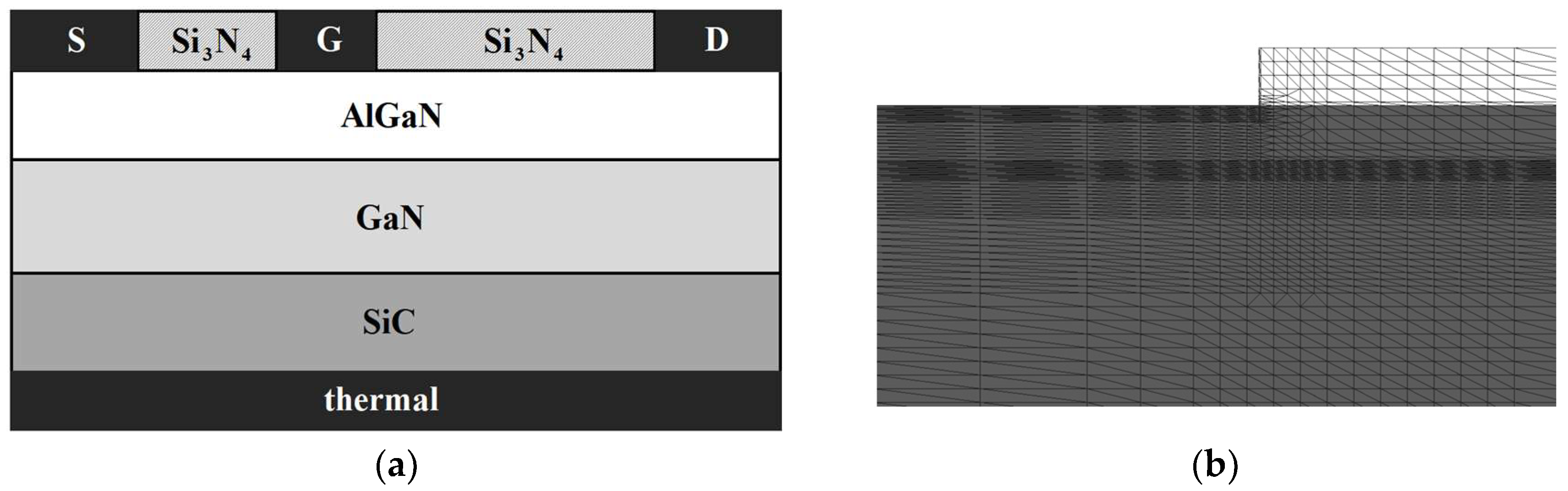
2. Materials and Methods

To investigate the impacts of traps on self-heating effects and the terahertz response in HEMTs, this study implemented a Sentaurus TCAD simulation framework. The SDE module was first employed for device structural modeling, establishing the HEMT configuration illustrated in Figure 1a, with channel-proximate mesh refinement detailed in Figure 1b. Following structural verification, a mesh file was generated.
Variations in aluminum (Al) composition within AlGaN induce spontaneous polarization by displacing positive and negative charge centers. At the AlGaN/GaN heterointerface, lattice mismatch generates piezoelectric polarization during epitaxial growth. The synergistic effect of these mechanisms establishes a built-in electric field within the AlGaN layer, causing electron accumulation and subsequent two-dimensional electron gas (2DEG) formation [19,20].
AlGaN layer thickness critically influences device performance:
  • Under-thinned layers (<25 nm) yield weak built-in fields, reducing 2DEG concentration and degrading conduction;
  • Over-thickened layers (>25 nm) diminish gate control efficacy, attenuating the terahertz response.
For this simulation, AlGaN thickness was optimized at 25 nm following Zhang et al.’s methodology. The remaining structural parameters are summarized in Table 1.
Two fundamental electrical contact types exist between electrodes and materials: Ohmic and Schottky contacts. To establish conductive paths between channel and source/drain electrodes, heavy doping creates Ohmic contacts [21]. Conversely, the gate electrode utilizes Schottky contacts to minimize leakage current [22]. The thermal electrode at the substrate interface provides thermal boundary conditions, maintained at 300 K throughout simulations.
Subsequently, Sentaurus TCAD (invoked via SDevice) implemented critical physical models. Carrier mobility, high-field saturation effects, and doping considerations were incorporated. Given that doping was solely employed for source/drain Ohmic contact formation—exhibiting negligible influence on channel electrical properties—and comparative simulations revealed minimal performance differences between mobility models, the computationally efficient Constant Mobility model was selected over the Doping Dependence model.
The mobility of the Constant Mobility model μ c o n s t only depends on the lattice temperature [23]:
μ c o n s t = μ L T 300 K ζ
where μ L is the mobility due to bulk phonon scattering. The default values of μ L and the exponent ζ are listed in Table 2. When the material is changed to AlGaAs, the default values of μ L and the exponent ζ will change too.
Before investigating the self-heating effect and terahertz response, the electrical characteristics of the device should be tested to ensure the correctness of its fundamental electrical properties and operational integrity.
Under zero gate bias, the drain-source voltage was swept from 0   V to 10   V to characterize conduction properties. Maintaining a constant DC source/drain voltage, the gate voltage was subsequently swept from 8   V to 4   V to evaluate transfer characteristics.
To explore the self-heating effect under different trap concentrations, as shown in Figure 2a, a pulse signal was configured in SDevice with an amplitude of 5 V, a delay time ( T d ) of 1.0 × 10 8   s , rise and fall times ( T r = T f ) of 5.0 × 10 7 s, a pulse width ( p w ) of 5.0 × 10 7   s , and a pulse period of 1.6 × 10 6 s. Since Sentaurus simulations may struggle to converge when abrupt boundary condition changes occur at the start, the delay time ( T d ) was introduced to allow the pulse to activate only after a brief simulation warm-up period.
A configured pulse was applied across the device source and drain while varying the trap concentration in the SDevice simulation environment. The analysis of channel current waveforms under different trap concentrations quantified trap concentration’s effects on self-heating, followed by a mechanistic investigation.
Simulation experiments revealed a strong convergence in the HEMT model at a trap concentration of 1 × 10 15   c m 3 . Consequently, all subsequent investigations of gate voltage effects on the terahertz response employed a consistent trap concentration of 1 × 10 15   c m 3 . As Figure 2b illustrates, the simulated waveform represents terahertz wave incidence with amplitude U W = 400 m V , period T w = 1 × 1 0 11   s , and corresponding frequency f w = 100 G H z —parameters within the terahertz band (0.1–10 THz). During terahertz radiation exposure, gate voltage sweeps were performed to analyze their impact on device response and underlying physical mechanisms.

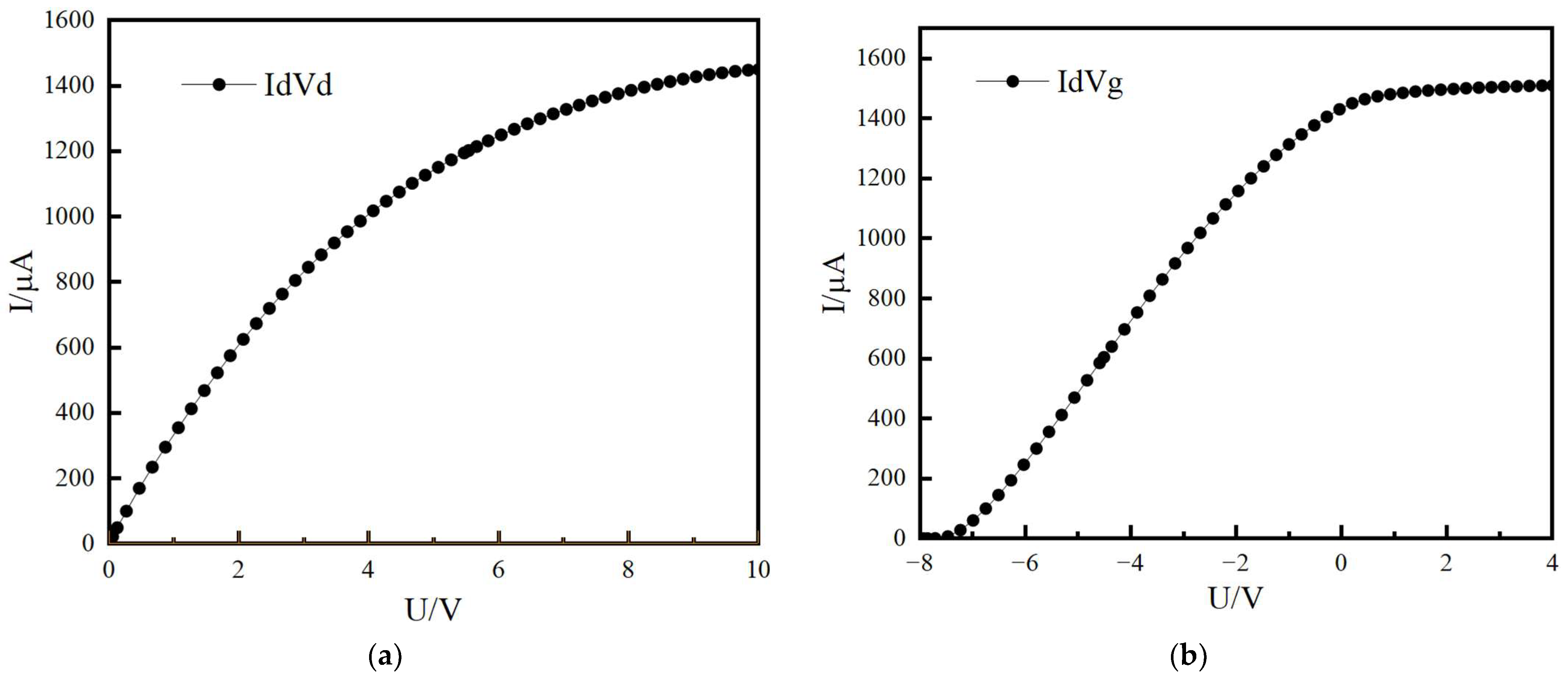
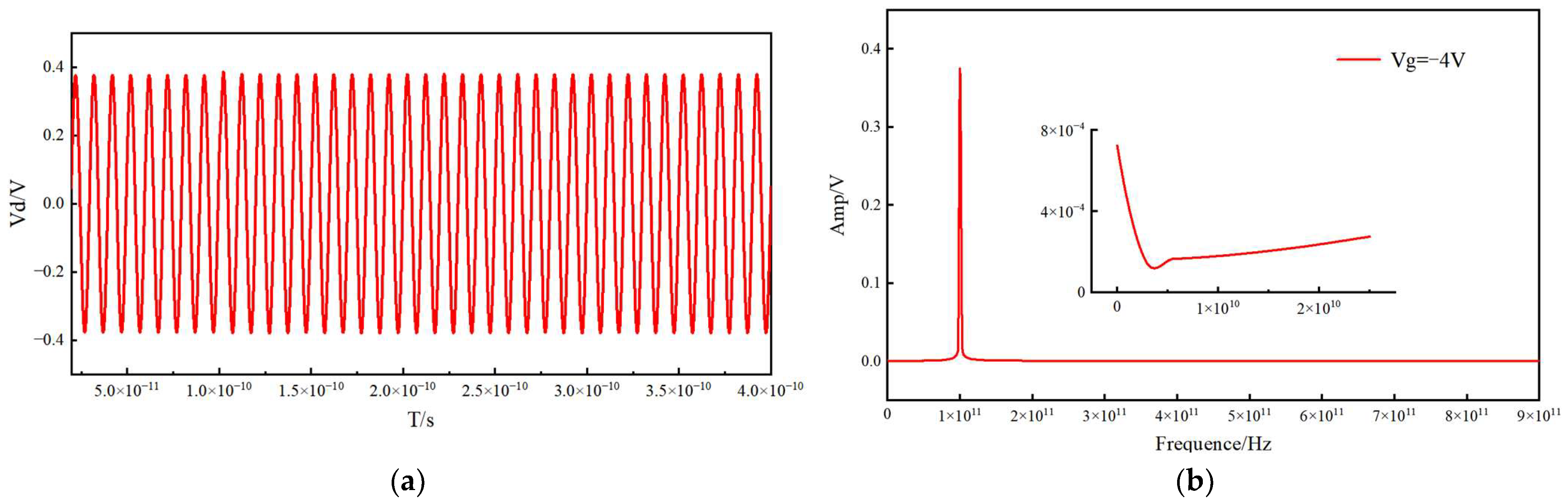
3. Results and Discussion
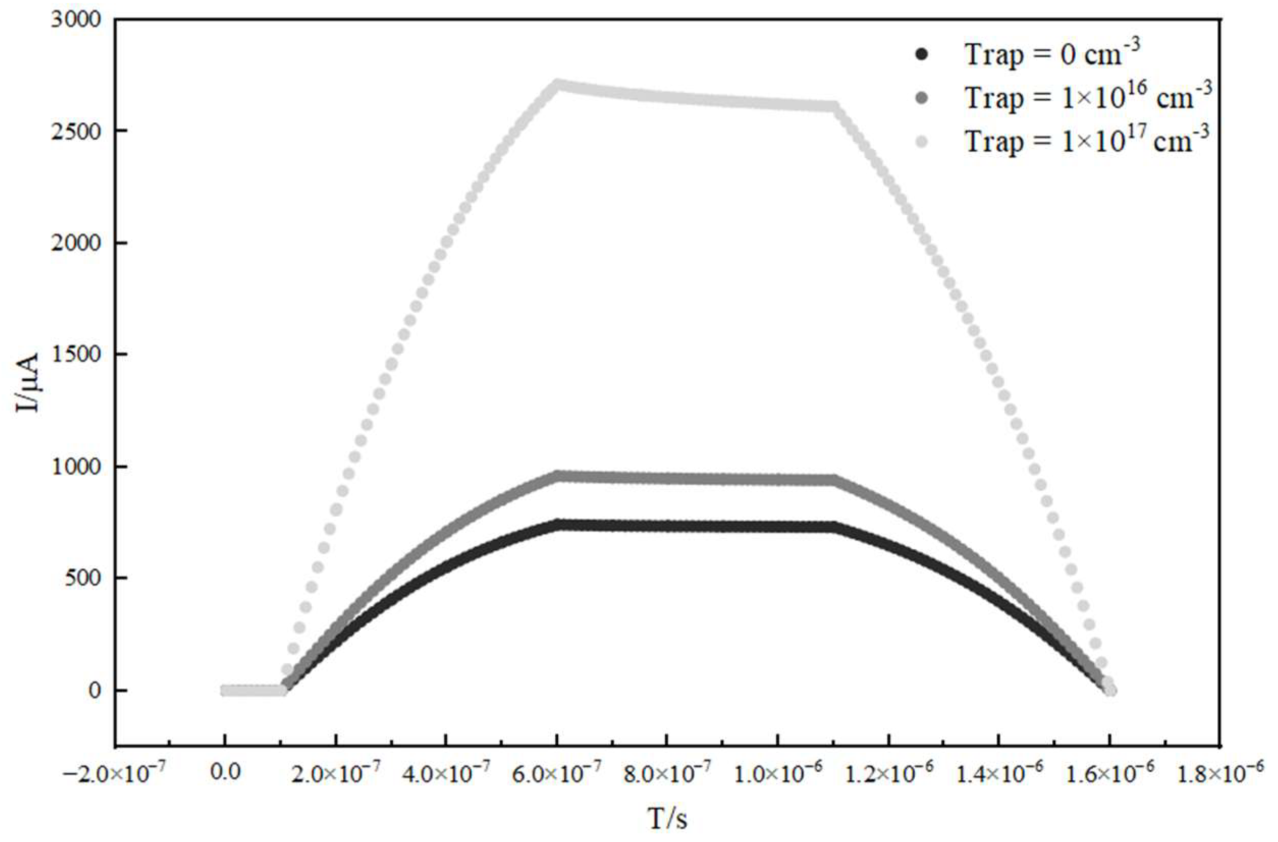
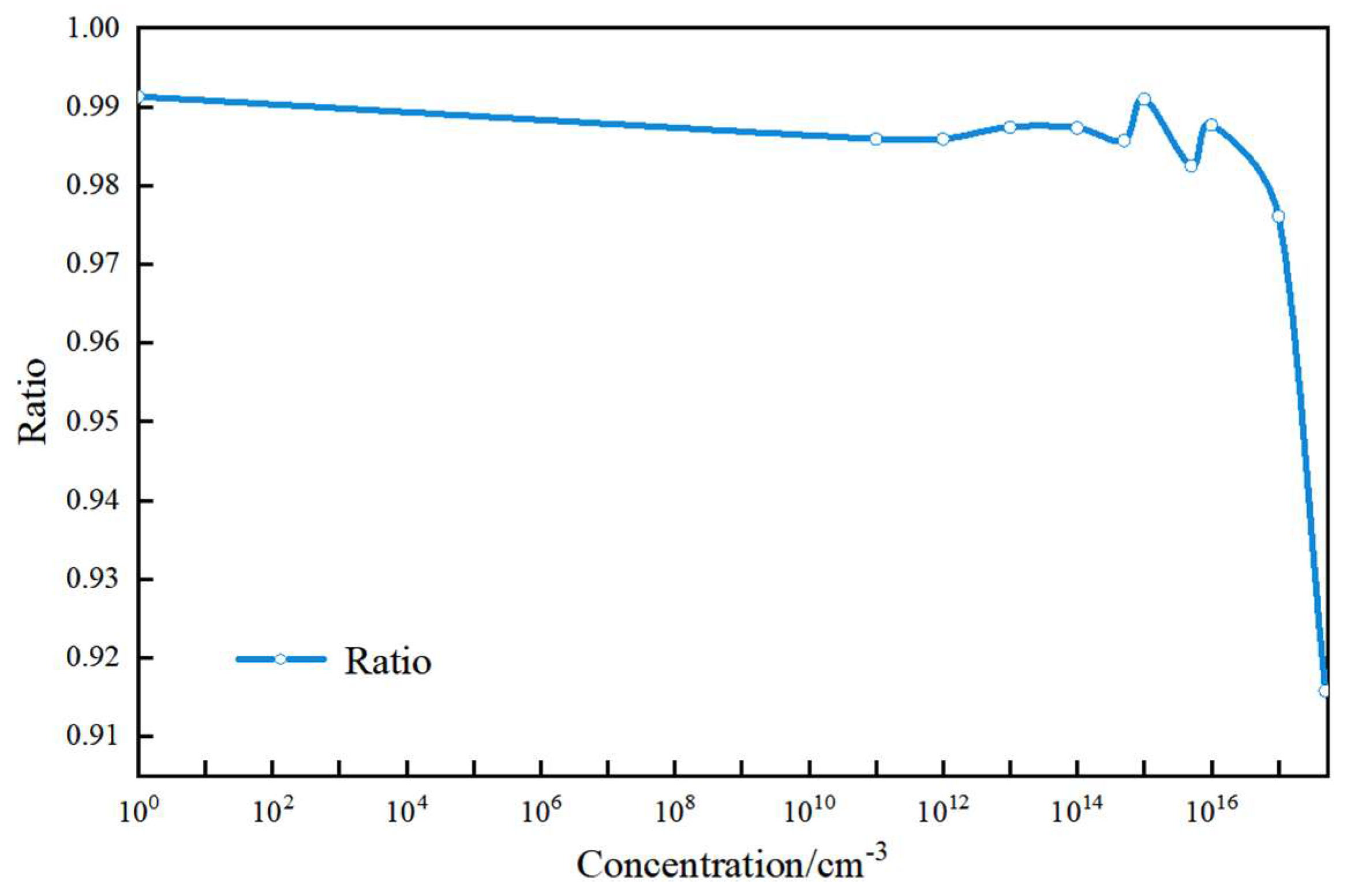
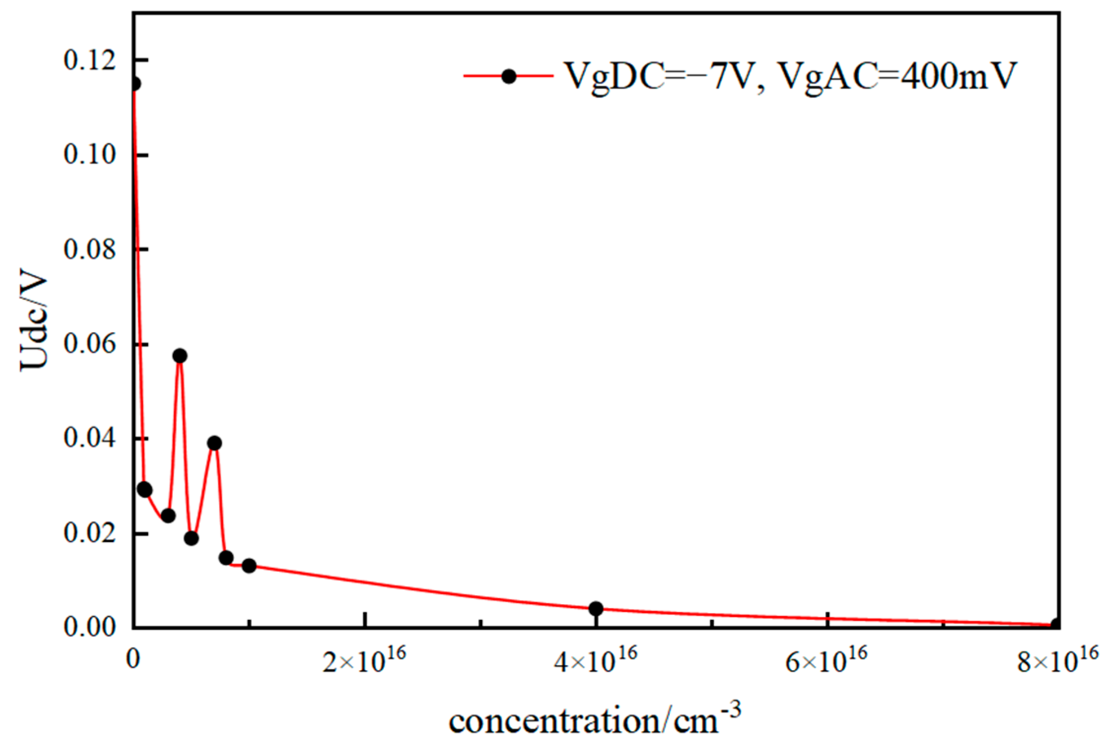
The fundamental electrical characteristics of the device are presented in Figure 3. During source/drain conduction characterization, channel current saturation occurs when the drain/source voltage reaches 10   V , consistent with high-field saturation behavior. For transfer characteristic measurements, the saturation voltage determined from conduction analysis ( 10   V ) was applied between the source and the drain. The channel approached cutoff conditions when gate voltage was reduced to 8   V , resulting in zero channel current. Positive gate voltages produced only a modest enhancement of channel current.
The self-heating effect manifests as degraded carrier mobility with increasing channel temperature, causing current collapse within single-pulse operation. Although multiple mitigation strategies exist [24,25,26], this work specifically examines trap-mediated effects. As demonstrated in Figure 4, elevated trap concentrations yield greater channel current enhancement. This improvement originates from trap-induced energy levels that extend carrier lifetime, thereby increasing channel carrier concentration. The capture rate c i and emission rate e i of these trap states are governed by
e i = c i g exp ( E t r a p E F i k T i ) ,
Here, E t r a p is the energy of the trap, E F i is the Fermi energy of the electronic reservoir, T i is the temperature of the reservoir, and g is the degeneracy factor. When the trap energy level ( E t r a p ) approaches the electron Fermi level ( E F i ), the emission rate of the trap level becomes lower than its capture rate. This leads to electron trapping, thereby increasing the carrier lifetime. When the trap concentration reaches 1 × 1 0 17   c m 3 , the channel current is almost three times that of a device without traps.
Figure 4. Manifestation of self-heating effects. Id curve when the pulse in Figure 2a has an effect on S and D at different trap concentrations.
Photonics 12 00719 g004
During the pulse width ( p w ) period, devices with varying trap concentrations all exhibit temporally dependent current collapse. It is observed that higher trap concentrations produce more pronounced absolute values of channel current collapse. As summarized in Table 3, devices with elevated trap concentrations show greater differentials between I d m a x and I d m i n .
However, the absolute magnitude of current collapse cannot serve as a criterion for determining whether the self-heating effect is mitigated or exacerbated. Here, we define the degree of current collapse as the ratio of I d m i n to I d m a x . A smaller ratio indicates a more severe current collapse. By correlating each obtained ratio with its corresponding trap concentration, we establish the trend shown in Figure 5.
The current collapse exhibits a “three-stage” variation with increasing trap concentration.
Specifically,
  • In a low concentration range (0 to 1 × 10 14   c m 3 ), the current collapse trend is negligible;
  • In an intermediate concentration range ( 1 × 10 14 to 1 × 10 16   c m 3 ), the current collapse fluctuates, peaking at a trap concentration of 1 × 10 15   c m 3 ;
  • In a high concentration range ( > 1 × 10 16   c m 3 ), the current collapse intensifies significantly, showing a clear degradation trend.
Simulation results demonstrated a strong convergence for devices with a trap concentration of 1 × 10 15   c m 3 . Current collapse trend analysis revealed that introducing traps at this concentration produces the least pronounced exacerbation of device self-heating. Consequently, among approaches employing traps to enhance conduction characteristics, a trap concentration of 1 × 10 15   c m 3 yields optimal DC operational efficiency.
Conventional theory dictates that the upper frequency limit of field-effect transistors (FETs) is governed by electron transit time. For the GaN HEMT devices simulated in this work, plasma wave theory within the two-dimensional electron gas (2DEG) framework explains the observed phenomena [27,28,29].
The 2DEG concentration in the device channel is modulated by the gate-to-channel voltage V g s , expressed as
n s = C V g s / q ,
where C is the gate-to-channel capacitance per unit area, and q is the elementary charge. The two-dimensional electron gas can be treated as a hydrodynamic fluid model. Consequently, the propagation of plasma waves can be described using the Euler equation for carriers and the current continuity equation [28]:
v t + v v x + q m U x + v τ = 0 ,
v t 1 q j n x = 0 ,
Here, v is the local electron velocity, m is the effective electron mass, U / x is the longitudinal electric field in the channel, τ is the momentum relaxation time, and j n is the current density.
HEMT devices exhibit two distinct detection modes: resonant and non-resonant detection. Resonant detection occurs when ω τ > > 1 , whereas non-resonant detection corresponds to a condition in which ω τ < < 1 , with ω representing the angular frequency of the incident wave. For the 0.1 THz frequency range examined in this study, the non-resonant detection criterion is satisfied.
When an alternating current (AC) signal is applied as the electrical boundary condition (illustrated in Figure 6) and the channel length L satisfies the long-channel condition, plasma waves generate a direct current (DC) component U d c between the source and the drain. This component is expressed as
U d c = U w 2 4 U 0 1 + 2 ω τ 1 + ω τ 2 ,
The long-channel criterion is given by
L > > s τ / ω ,
U w is the amplitude of AC signal, and U 0 = V g s V t h , where V t h means the threshold voltage of the device. For a signal frequency of 0.1 THz, devices with a channel length exceeding 600 nm can be classified as long-channel devices.
Following the theoretical framework of this study, the drain was configured with a current boundary condition—one of the fundamental modes for simulating terahertz detection. Trap densities were initialized at 1 × 10 15   c m 3 , V g D C = 4   V , and V g A C = 400   m V , as specified in Figure 6. Figure 7a clearly demonstrates an alternating current oscillating at the terahertz frequency of 100 GHz. Concurrently, Figure 7b reveals a small direct current component (724.13 μV) through Fast Fourier Transform (FFT) analysis, which constitutes the characteristic signature of terahertz detection.
As demonstrated in the preceding analysis, traps exert a profound influence on the thermodynamic framework and self-heating phenomena. Given that terahertz (THz) radiation inherently contributes to power dissipation, traps further exert discernible impacts on THz detection performance. In Figure 8a, the degradation effect of traps in terahertz detection is clearly observed through the wide range of V g . In addition, with the density of traps ( 1 × 10 15   c m 3 ), the relationship between U d c and V g D C shows the non-monotonic signature which is widely observed in most of the terahertz simulations [29,30,31]. The maximum value of U d c is 0.12 V at V g D C = 7.8   V when traps of 1 × 10 15   c m 3 are present. It is verified that the trap-free configuration exhibits characteristics similar to the case with 1 × 10 15   c m 3 traps. Figure 8b reveals a systematic degradation of U d c across the operational range, with peak degradation (64.89% reduction) observed at V g D C = 4.9   V under trap-free conditions.
Equations (2) and (6) demonstrate that the discrepancy in terahertz detection performance between the 1 × 10 15   c m 3 trap density case and the trap-free scenario arises from variations in the parameter τ (all other simulation parameters being identical). As Equation (7) indicates, GaN HEMT operation in non-resonant mode results in ω τ 1 . Under this condition, traps capture electrons, leading to increased ω τ and consequently higher DC. However, the simulation results deviate from the theoretical calculations due to externally induced electric fields originating from temperature gradients, which are substantially enhanced in the 1 × 10 15   c m 3 trap density model.
In the next section, the effect of different densities of traps on U d c degradation is simulated. In this section, due to the bigger U d c near the threshold voltage, V g D C = 7   V and V g A C = 400   m V are effectted. In Figure 9, some characteristic has been clearly shown:
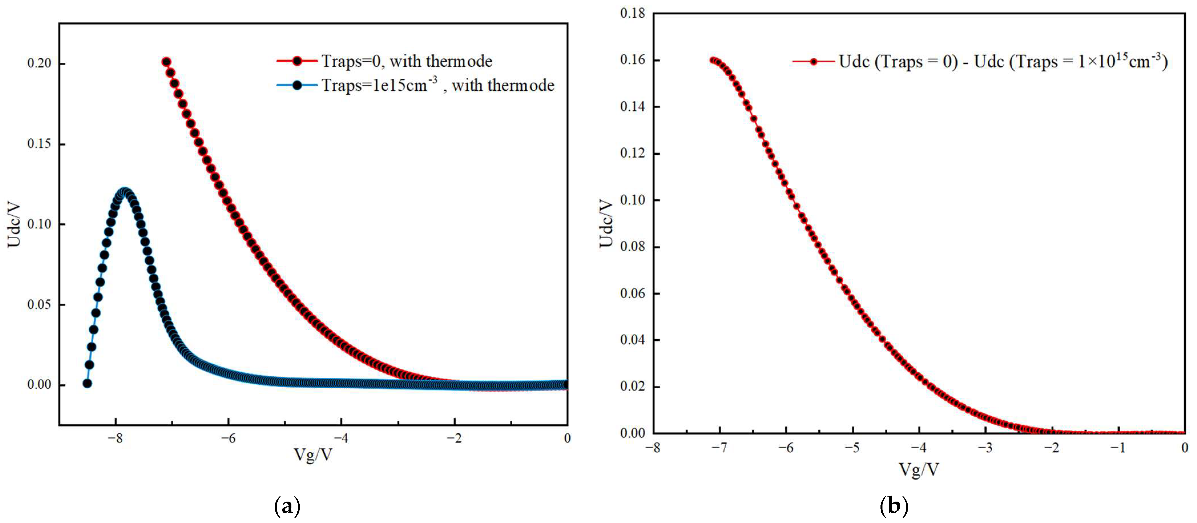
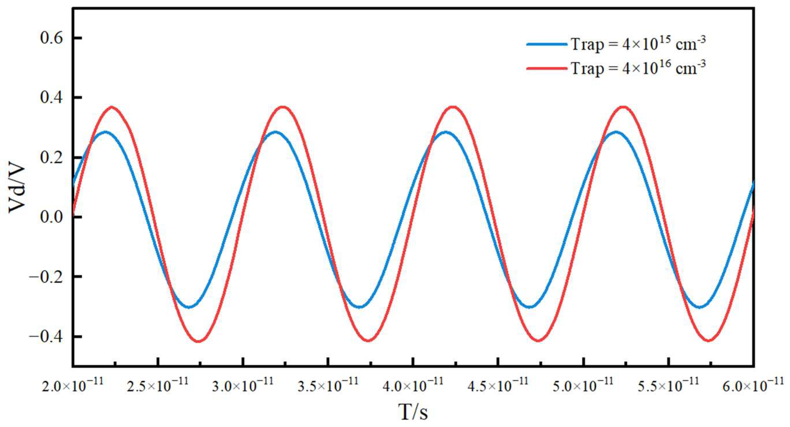
  • A larger trap density leads to more sever degradation in U d c ;
  • Two maximum values are observed at trap densities of 4 ×   10 15   c m 3 and 7 ×   10 15   c m 3 .
The non-monotonic feature is novel in terahertz detection. Figure 10 shows trap densities of 4 ×   10 15   c m 3 and 4 ×   10 16   c m 3 . A larger oscillation voltage is observed in the device with a trap density of 4 ×   10 15   c m 3 and leads to a larger DC voltage, which is the maximum value in Figure 9.

4. Conclusions

Based on Sentaurus TCAD simulation results, key conclusions regarding the design of GaN-based HEMT power devices were derived. Traps significantly enhance the channel current by extending the carrier lifetime through the introduction of new energy levels, achieving a current gain of up to threefold at a concentration of 1 × 10 17   c m 3 . However, when introducing traps to improve DC conduction performance, their concentration should not exceed optimal levels. At trap concentrations above 1 × 10 16 cm−3, current collapse severity increases sharply and pronounced device self-heating occurs. This leads to thermal accumulation in the channel, consequently degrading the power conversion efficiency.
Regarding terahertz response characteristics, concentration-dependent and gate-bias-dependent trends were observed. Increasing trap concentration generally reduces terahertz response U d c , though notable fluctuations occur near concentrations of 4 ×   10 15   c m 3 and 1 × 10 17   c m 3 . Therefore, where traps are unavoidable in device fabrication, introducing an optimized trap concentration may improve terahertz response performance. Similarly, for trap-affected devices, gate voltage selection should avoid regions of significant terahertz response degradation. When designing operating gate voltages, the simulation methodology presented herein enables modeling the terahertz response versus gate voltage characteristic under actual trap concentrations. This facilitates the characterization of terahertz response degradation across gate voltages, providing critical guidance for determining reference gate bias conditions.

Author Contributions

Conceptualization, H.F. and X.W. (Xiaoyun Wang); methodology, X.W. (Xiaoyun Wang); software, X.W. (Xiaoyun Wang) and X.W. (Xiaofang Wang); validation, H.F.; formal analysis, X.W. (Xiaoyun Wang); investigation, H.F.; data curation, H.F. and X.W. (Xiaofang Wang); writing—original draft preparation, H.F.; writing—review and editing, H.F.; visualization, H.F.; supervision, L.W. and X.W. (Xiaofang Wang); project administration, L.W. All authors have read and agreed to the published version of the manuscript.

Funding

This research received no external funding.

Data Availability Statement

Data are contained within the article.

Conflicts of Interest

The authors declare no conflict of interest.

References

  1. Quast, H.; Loffler, T. 3D-terahertz-tomography for material inspection and security. In Proceedings of the 2009 34th International Conference on Infrared, Millimeter, and Terahertz Waves, Busan, Republic of Korea, 21–25 September 2009. [Google Scholar]
  2. Liu, J.; Dai, J.; Chin, S.L.; Zhang, X.-C. Broadband terahertz wave remote sensing using coherent manipulation of fluorescence from asymmetrically ionized gases. Nat. Photonics 2010, 4, 627–631. [Google Scholar] [CrossRef]
  3. Yang, Y.; Yamagami, Y.; Yu, X.; Pitchappa, P.; Webber, J.; Zhang, B.; Fujita, M.; Nagatsuma, T.; Singh, R. Terahertz topological photonics for on-chip communication. Nat. Photonics 2020, 14, 446–451. [Google Scholar] [CrossRef]
  4. Li, X.; Li, J.; Li, Y.; Ozcan, A.; Jarrahi, M. High-throughput terahertz imaging: Progress and challenges. Light Sci. Appl. 2023, 12, 233. [Google Scholar] [CrossRef]
  5. Hou, H.W.; Liu, Z.; Teng, J.H.; Palacios, T.; Chua, S.J. High Temperature Terahertz Detectors Realized by a GaN High Electron Mobility Transistor. Sci. Rep. 2017, 7, 46664. [Google Scholar] [CrossRef]
  6. Bauer, M.; Ramer, A.; Chevtchenko, S.A.; Osipov, K.Y.; Cibiraite, D.; Pralgauskaite, S.; Ikamas, K.; Lisauskas, A.; Heinrich, W.; Krozer, V.; et al. A High-Sensitivity AlGaN/GaN HEMT Terahertz Detector with Integrated Broadband Bow-Tie Antenna. IEEE Trans. Terahertz Sci. Technol. 2019, 9, 430–444. [Google Scholar] [CrossRef]
  7. An, N.; Li, L.; Wang, W.; Xu, X.; Zeng, J. High-Efficiency D-Band Monolithically Integrated GaN SBD-Based Frequency Doubler with High Power Handling Capability. IEEE Trans. Electron Devices 2022, 69, 4843–4847. [Google Scholar] [CrossRef]
  8. Wang, C.; Luo, J.; Zhang, Z.; Gu, C.; Zhu, H.; Zhang, L. A 2.0–3.0 GHz GaN HEMT-Based High-Efficiency Rectifier Using Class-EFJ Operating Mode. Electronics 2024, 13, 2786. [Google Scholar] [CrossRef]
  9. Saidi, I.; Gassoumi, M.; Maaref, H.; Mejri, H.; Gaquière, C. Self-heating and trapping effects in AlGaN/GaN heterojunction field-effect transistors. J. Appl. Phys. 2009, 106, 054511. [Google Scholar] [CrossRef]
  10. Arivazhagan, L.; Jarndal, A.H.M.; Chander, S.; Godfrey, D.; Kumar, J.R.; Bhagyalakshmi, S.; Reddy, P.K.; Nirmal, D. Self-Heating Analysis of GaN-HEMT for Various Ambient Temperature and Substrate Thickness. In Proceedings of the 2020 5th International Conference on Devices, Circuits and Systems (ICDCS), Coimbatore, India, 5–6 March 2020. [Google Scholar]
  11. Chen, X.; Boumaiza, S.; Wei, L. Modeling Bias Dependence of Self-Heating in GaN HEMTs Using Two Heat Sources. IEEE Trans. Electron Devices 2020, 67, 3082–3087. [Google Scholar] [CrossRef]
  12. Kebir, M.E.; Bri, S. Self-Heating in the HEMT AlGaN/GaN transistor. In Proceedings of the 2020 IEEE 2nd International Conference on Electronics, Control, Optimization and Computer Science (ICECOCS), Kenitra, Morocco, 2–3 December 2020. [Google Scholar]
  13. Tang, Z.L.; Shen, Y.; Cao, B.Y. Modulating Self-Heating Effects in GaN HEMTs Using Slant Field Plate. IEEE Trans. Electron Devices 2025, 72, 1907–1911. [Google Scholar] [CrossRef]
  14. Kalavagunta, A.; Mukherjee, S.; Reed, R.; Schrimpf, R. Comparison between trap and self-heating induced mobility degradation in AlGaN/GaN HEMTs. Microelectron. Reliab. 2014, 54, 570–574. [Google Scholar] [CrossRef]
  15. Zhang, Y.; Shiwei, F.; Hui, Z.; Xueqin, G.; Bing, D.; Lin, M. Self-heating and traps effects on the drain transient response of AlGaN/GaN HEMTs. J. Semicond. 2014, 35, 104003. [Google Scholar] [CrossRef]
  16. Maryam, S.; Peiman, A. Influence of the Passivation Layers on the Self-Heating Effect in the Double Channel AlGaN/GaN MOS-HEMT Device. Russ. Microelectron. 2023, 52, 112–118. [Google Scholar] [CrossRef]
  17. Nasir, A.; Zhang, X.; Lu, L.; Zhang, J.; Lyu, J.; Cui, Y. Enhanced crystalline quality of non-polar a-plane AlGaN epitaxial film grown with Al-composition-graded AlGaN intermediate layer. Mater. Res. Express 2021, 8, 055901. [Google Scholar] [CrossRef]
  18. Zou, X.; Yang, J.; Qiao, Q.; Zou, X.; Chen, J.; Shi, Y.; Ren, K. Trap Characterization Techniques for GaN-Based HEMTs: A Critical Review. Micromachines 2023, 14, 2044. [Google Scholar] [CrossRef]
  19. He, X.-G.; Zhao, D.-G.; Jiang, D.-S. Formation of two-dimensional electron gas at AlGaN/GaN heterostructure and the derivation of its sheet density expression*. Chin. Phys. B 2015, 24, 067301. [Google Scholar] [CrossRef]
  20. Lingaparthi, R.; Dharmarasu, N.; Radhakrishnan, K.; Ranjan, A.; Seah, T.L.A.; Huo, L. Source of two-dimensional electron gas in unintentionally doped AlGaN/GaN multichannel high-electron-mobility transistor heterostructures. Appl. Phys. Lett. 2021, 118, 122105. [Google Scholar] [CrossRef]
  21. Greco, G.; Iucolano, F.; Roccaforte, F. Ohmic contacts to Gallium Nitride materials. Appl. Surf. Sci. 2016, 383, 324–345. [Google Scholar] [CrossRef]
  22. Kim, H. Vertical Schottky Contacts to Bulk GaN Single Crystals and Current Transport Mechanisms: A Review. J. Electron. Mater. 2021, 50, 6688–6707. [Google Scholar] [CrossRef]
  23. Ha, M.-W.; Seok, O.; Lee, H.; Lee, H.H. Mobility Models Based on Forward Current-Voltage Characteristics of P-type Pseudo-Vertical Diamond Schottky Barrier Diodes. Micromachines 2020, 11, 598. [Google Scholar] [CrossRef]
  24. Nasir, A.; Xu, B.; Ali, I.; Akbar, J. Improvements in structural and optical properties of nonpolar a-plane AlGaN epilayers with nanoscale island-like SiNx interlayer. J. Mater. Sci. Mater. Electron. 2023, 34, 60. [Google Scholar] [CrossRef]
  25. Sani, H.; Khosroabadi, S. Improving Thermal Effects and Reduction of Self-heating Phenomenon in AlGaN/GaN/Si Based HEMT. J. Electron. Mater. 2021, 50, 2295–2304. [Google Scholar] [CrossRef]
  26. Kumar, A.; Gupta, A.; Rai, S. Reduction of self-heating effect using selective buried oxide (SELBOX) charge plasma based junctionless transistor. AEU-Int. J. Electron. Commun. 2018, 95, 162–169. [Google Scholar] [CrossRef]
  27. Dyakonov, M.; Shur, M. Detection, mixing, and frequency multiplication of terahertz radiation by two-dimensional electronic fluid. IEEE Trans. Electron Devices 1996, 43, 380–387. [Google Scholar] [CrossRef]
  28. Dyakonov, M.; Shur, M. Shallow water analogy for a ballistic field effect transistor: New mechanism of plasma wave generation by dc current. Phys. Rev. Lett. 1993, 71, 2465–2468. [Google Scholar] [CrossRef] [PubMed]
  29. Meng, Q.; Lin, Q.; Jing, W.; Han, F.; Zhao, M.; Jiang, Z. TCAD Simulation for Nonresonant Terahertz Detector Based on Double-Channel GaN/AlGaN High-Electron-Mobility Transistor. IEEE Trans. Electron Devices 2018, 65, 4807–4813. [Google Scholar] [CrossRef]
  30. Nasir, A.; Zhang, X.; Zakria, M.; Zhang, J.; Hu, G.; Cui, Y. Effect of NH3-flow modulation on the morphological properties of nonpolar a-plane AlGaN epilayers. Superlattices Microstruct. 2021, 159, 107045. [Google Scholar] [CrossRef]
  31. Zhu, Y.; Ji, X.; Liao, Y.; Wu, F.; Yan, F. TCAD simulation of gate-enclosed MOSFET for terahertz detector. In Proceedings of the 2014 12th IEEE International Conference on Solid-State and Integrated Circuit Technology (ICSICT), Guilin, China, 28–31 October 2014. [Google Scholar]
Figure 1. (a) The structure of HEMT constructed by SDE, (b) The mesh of device.
Photonics 12 00719 g001
Figure 2. Effect of pulse waveform on the electrode. (a) shows the waveform of the effect of periodic pulse V d s between the drain and the source; (b) explains the terahertz waveform, which has been effected on the gate.
Photonics 12 00719 g002
Figure 3. Electrical characteristic test results: (a) characteristic of I d V d curve; (b) characteristic of I d V g curve.
Photonics 12 00719 g003
Figure 5. The trend of the min-to-max current ratio within the pulse width ( p w ) duration.
Photonics 12 00719 g005
Figure 6. The scheme of terahertz detection by GaN HEMT.
Photonics 12 00719 g006
Figure 7. The figure shows the time-domain waveform and spectral characteristics of the source/drain voltage. Figure (a) displays the V-T characteristic curve of the source/drain voltage under conditions of a trap concentration of 1 × 10 15   c m 3 , V g D C = 7   V , and V g A C = 400   m V . Figure (b) presents the FFT (Fast Fourier Transform) result derived from Figure (a).
Photonics 12 00719 g007
Figure 8. The figure demonstrates the variation curve of the terahertz DC response between the source and drain under different V g D C conditions. Figure (a) shows the relationship between the response intensity and V g D C at trap concentrations of 0 and 1 × 15   c m 3 . Figure (b) displays the vertical axis difference between the two curves in Figure (a).
Photonics 12 00719 g008
Figure 9. The figure illustrates the variation trend of the DC component in the terahertz response between the source and drain as the trap concentration increases.
Photonics 12 00719 g009
Figure 10. The waveform of V d s when V g D C = 7   V at trap concentration = 4 ×   10 15   c m 3 and trap concentration = 4 × × 10 16   c m 3 .
Photonics 12 00719 g010
Table 1. Parameters and materials of layers in HEMT model.
Material/ContactThickness ( μ m )Width ( μ m )
S i 3 N 4 (S side)0.0251.5
S i 3 N 4 (D side)0.0252.2
A l G a N 0.0255.9
G a N 25.9
S i C 105.9
Electrode S0.5
Electrode G1
Electrode D0.5
thermal5.9
Table 2. Constant mobility model: default coefficients for silicon.
SymbolElectronsHolesUnit
μ L 1417470.5 c m 2 / V s
ζ2.52.21
Table 3. Min-to-max current ratio within the pulse width duration.
Trap Concentration ( c m 3 ) I d m a x ( μ A ) I d m i n ( μ A ) I d m i n / I d m a x
0738.7534732.33480.9913
1 × 10 11 742.8229732.33650.9859
1 × 10 12 742.8384732.35160.9859
1 × 1 0 13 742.9932733.60270.9874
1 × 1 0 14 744.5444735.12050.9873
5 × 1 0 14 751.5934740.85720.9857
1 × 1 0 15 756.6317749.83050.9910
5 × 1 0 15 848.5516833.72050.9825
1 × 1 0 16 953.7343942.08890.9877
1 × 1 0 17 2677.8082613.8270.9761
5 × 1 0 17 8478.1597763.9490.9158
Disclaimer/Publisher’s Note: The statements, opinions and data contained in all publications are solely those of the individual author(s) and contributor(s) and not of MDPI and/or the editor(s). MDPI and/or the editor(s) disclaim responsibility for any injury to people or property resulting from any ideas, methods, instructions or products referred to in the content.

