Article

Gain Characteristics of Hybrid Waveguide Amplifiers in SiN Photonics Integration with Er-Yb:Al2O3 Thin Film

by
Ziming Dong
,
Guoqing Sun
,
Yuqing Zhao
,
Yaxin Wang
,
Lei Ding
,
Liqin Tang
and
Yigang Li
*
School of Physics, Nankai University, Tianjin 300071, China
*
Author to whom correspondence should be addressed.
Photonics 2025, 12(7), 718; https://doi.org/10.3390/photonics12070718
Submission received: 6 June 2025 / Revised: 12 July 2025 / Accepted: 14 July 2025 / Published: 16 July 2025

Abstract

Integrated optical waveguide amplifiers, with their compact footprint, low power consumption, and scalability, are the basis for optical communications. The realization of high gain in such integrated devices is made more challenging by the tight optical constraints. In this work, we present efficient amplification in an erbium–ytterbium-based hybrid slot waveguide consisting of a silicon nitride waveguide and a thin-film active layer/electron-beam resist. The electron-beam resist as the upper cladding layer not only possesses the role of protecting the waveguide but also has tighter optical confinement in the vertical cross-section direction. On this basis, an accurate and comprehensive dynamic model of an erbium–ytterbium co-doped amplifier is realized by introducing quenched ions. A modal gain of above 20 dB is achieved at the signal wavelength of 1530 nm in a 1.4 cm long hybrid slot waveguide, with fractions of quenched ions fq = 30%. In addition, the proposed hybrid waveguide amplifiers exhibit higher modal gain than conventional air-clad amplifiers under the same conditions. Endowing silicon nitride photonic integrated circuits with efficient amplification enriches the integration of various active functionalities on silicon.

1. Introduction

Erbium-doped fiber amplifiers (EDFAs) with low nonlinearity, low noise, wide gain, and coverage of telecommunication C-band and L-band are the basis of long-distance optical communication at present [1]. Erbium-doped waveguide amplifiers (EDWAs) [2] are an important complement to EDFAs, which have seen remarkable development in recent years [3,4,5,6]. Compared with EDFAs, EDWAs can utilize an optical waveguide structure to achieve high signal optical gain near the operating wavelength within a tiny size, attributed to its higher erbium concentration [7]. Therefore, EDWAs are capable of planar and three-dimensional integration with other optical waveguide devices, constituting a high-efficiency dense integrated optical system [8,9,10]. Taken together, EDWAs not only inherit the advantages of EDFAs but also possess the characteristics of low loss, compact size, high stability, and compatibility [11,12,13], which are key to promoting the development of photonic integrated circuits [14,15,16].
The integrated silicon nitride (SiN) photonic platform is an ideal candidate for the sustainable development of EDWAs [17], and it has a wider transparent window and lower temperature cross-sensitivity than silicon [18]. Moreover, in the telecom band, two-photon absorption is negligible, with propagation loss as low as 3 dB/m [19]. Amplifiers on SiN photonic integrated circuits have the function of light emission and amplification, which provides the potential to integrate active devices, including high-performance lasers [20] and amplifiers [21,22,23], on the chip. Erbium-doped amplifiers based on low-loss SiN waveguides are attractive active devices and have been widely deployed in applications such as optical communications, precision measurements, and integrated microcombs [24,25,26]. Recent advances have designed diverse SiN waveguide amplifiers to achieve gain performance [7,21,22,23,27].
Addressing the hurdles of efficient amplification in integrated SiN photonic platforms, alternative approaches involving host materials have gained prominence, with aluminum (Al2O3) standing out for its advantages relating to high transparency, high rare-earth solubility, and moderate refractive index contrast for compact devices. Although Al2O3 features various significant advantages, its point defects introduce characteristic absorption edges in the near-infrared spectral region [28,29]. This parasitic absorption directly competes with Er ions for pump beams (980 nm), reducing pump efficiency and limiting population inversion. Additionally, these point defects facilitate non-radiative relaxation channels for excited Er ions, leading to their energy being released to the defects in the form of lattice vibrations. This induces a decrease in the fluorescence quantum efficiency of the telecommunication bands, ultimately reducing the net gain. Thus, Yb ions are usually added as sensitizers to enhance the pump absorption efficiency of EDWAs and to alleviate the concentration-quenching effect among erbium ions.
Nowadays, slot waveguides attract significant attention in the field of integrated optics [30,31,32]. This is because, compared to conventional ridge or strip waveguides [33], slot waveguides provide superior optical field confinement in the low-refractive-index slot region, enabling remarkable enhancement of light–matter interactions. This unique structure confines the optical field within a nano-scale slot, demonstrating great potential for fabricating high-performance integrated waveguide amplifiers. In a recent report, a slot waveguide amplifier formed by coating SiN waveguides with an atomic layer-deposited Er:Al2O3 film showed a high gain per unit length of 20.1 dB/cm [7]. Despite this great progress, only modest total gains have been obtained in waveguides with a length of less than 0.12 cm, limiting their practical use.
In this work, we present a hybrid SiN waveguide amplifier via integration with an erbium–ytterbium co-doped aluminum oxide (Er-Yb:Al2O3) layer and an upper cladding. The upper cladding-covered waveguide has tighter optical confinement in the vertical cross-section direction. According to accurate and comprehensive Er-Yb co-doped amplification dynamics modeling, the hybrid waveguide amplifier is carefully optimized with quenched ions. A modal gain of above 20 dB at the signal wavelength of 1530 nm pumped by 980 nm can be achieved when the erbium ion concentration is 3 × 1020 cm−3 and the ytterbium ion concentration is 2.4 × 1021 cm−3. This work provides theoretical support and optimization guidance for Er-Yb:Al2O3-cladded amplifiers based on SiN waveguides.

2. Structure Design and Simulation Optimization

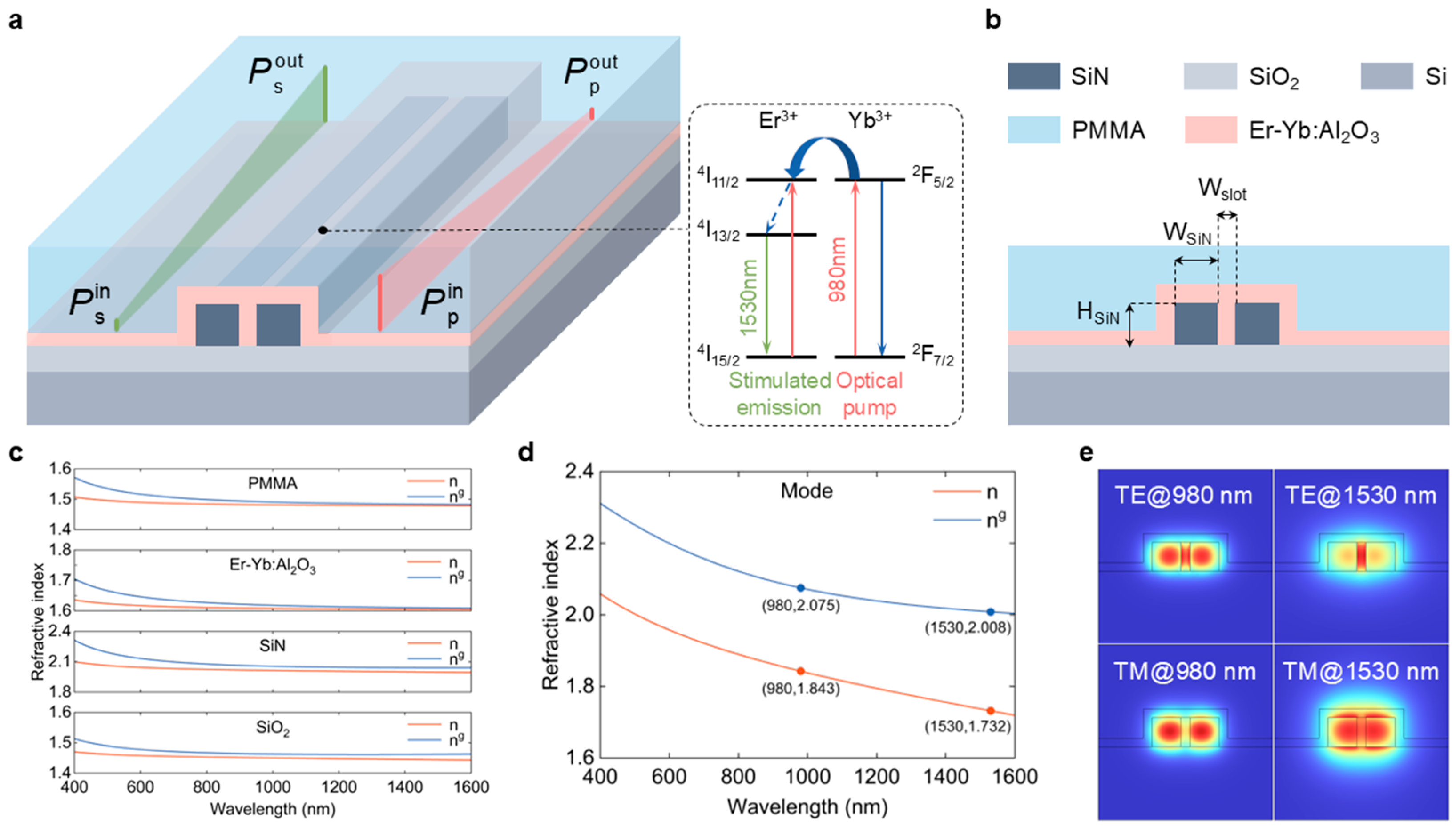
2.1. Characterization of the Hybrid Slot Waveguide

A schematic diagram of the cladded amplifier based on the Er-Yb co-doped hybrid slot waveguide is provided in Figure 1a. On the silicon dioxide substrate, two adjacent high refractive index contrasting passive SiN waveguides create a slot region, which is filled with an active Er-Yb:Al2O3 layer. The top PMMA layer acts as an upper cladding layer to further enhance the amplifier performance and protect the hybrid slot waveguide against damage. The working principle of the Er-Yb co-doped amplifier during stimulated emission is shown in the dashed box. Employing a 980 nm laser as the pump source is primarily due to the fact that the absorption cross section of Yb ions at this wavelength is larger than that of Er ions. The excited Yb ions transfer energy to the neighboring Er ions, contributing to a high power conversion efficiency. The input signal beam is amplified, while the pump beam is simultaneously attenuated in this process. Figure 1b shows a simplified cross section of the slot waveguide amplifier at the central axis. The key design parameters affecting waveguide performance are the slot waveguide width (Wslot), the slot waveguide height (HSiN), and the SiN waveguide width (WSiN). To be more accurate in the model calculations, the refractive indices of PMMA, Er-Yb:Al2O3, SiN, and SiO2 need to be known as a function of the wavelength. The refractive indices of these materials are obtained from references [34,35,36,37], and then the group refractive indices of each material are calculated by definition ng(λ) = n(λ) − λdn/, as exhibited in Figure 1c. Based on the above, Figure 1d demonstrates the calculated effective mode index and the effective group index of the fundamental transverse electric (TE) mode corresponding to the hybrid waveguide cross section at the same wavelength range. Before optimization, the TE and transverse magnetic (TM) fundamental mode electric field distributions of the waveguide at λ = 980 nm and λ = 1530 nm are calculated by setting Wslot = 150 nm, HSiN = 500 nm, and WSiN = 500 nm, as depicted in Figure 1e. The electric field distribution of the fundamental mode indicates that both polarizations can be confined within the waveguide cross section. However, the TE mode is more confined to the slot region of the active gain medium. Therefore, to obtain the highest possible gain, only the TE mode is investigated in subsequent calculations.

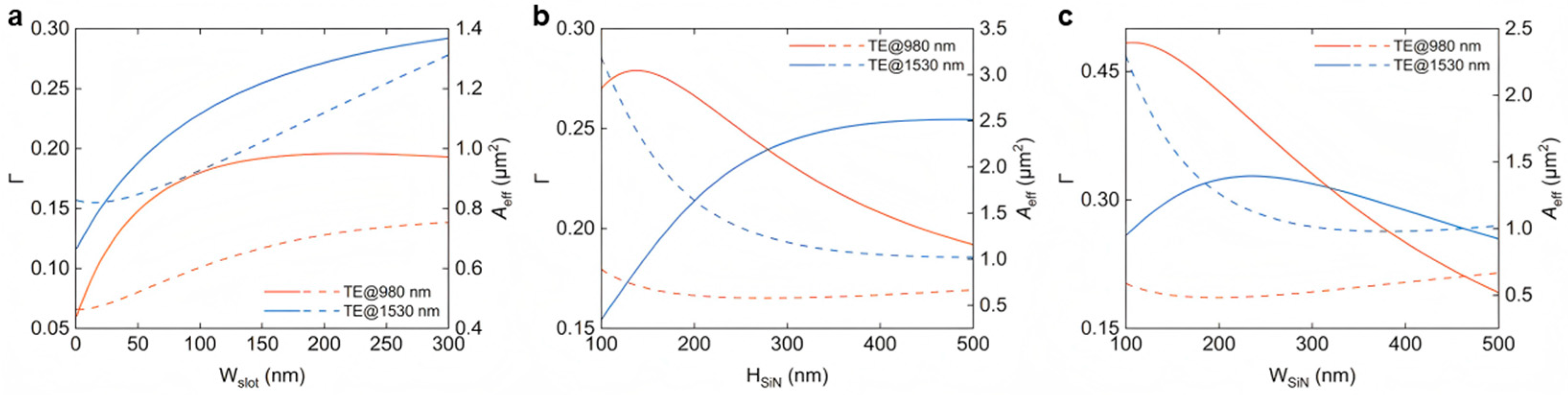
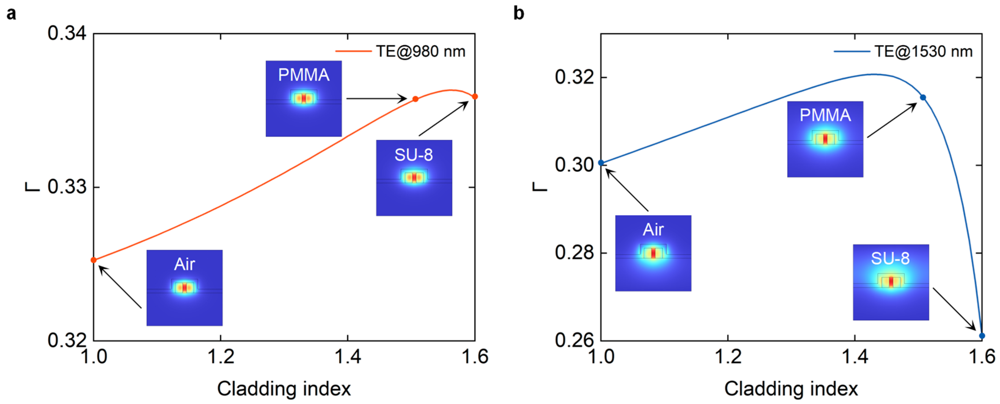
2.2. Optimization of the Hybrid Slot Waveguide

An essential feature of hybrid slot waveguide design is the effect on beam propagation by the slot waveguide width. In order to enhance the light interaction with the active layer, a hybrid slot waveguide amplifier was designed based on the finite element method, and the structure is further optimized according to the electric field mode distribution. The mode confinement factor Γ and the effective mode area Aeff in the active region of the waveguide are calculated as accurately as possible by considering the material dispersion and modal component contribution [7].
Figure 2a represents the dependence of the confinement factor (solid curve) and the effective mode area (dashed curve) on Wslot for the TE mode at λ = 980 nm and λ = 1530 nm, respectively. It can be seen that the confinement factor gradually increases as Wslot increases. When Wslot exceeds 150 nm, the confinement factor remains almost constant at about 0.19 at 980 nm, and the confinement factor exceeds 0.25 at 1530 nm. Notably, the growth rate of the mode confinement factor for the TE mode decreases significantly when Wslot exceeds 150 nm. Continuing to increase Wslot beyond 200 nm, the mode confinement factor exhibits a slight decline at 980 nm and increases by 0.02 at 1530 nm. Furthermore, the effective mode area dependence on Wslot illustrates that the effective mode area of the fundamental TE mode is less than 1 μm2 at both signal and pump wavelengths with Wslot less than 150 nm. In general, a small effective mode area facilitates the slot waveguide amplifier to achieve net gain at a low saturated input power. Therefore, in combination with the above analysis, optimized Wslot = 150 nm is selected for further study.
Another key feature of the SiN waveguide design is its cross-section dimensions. HSiN and WSiN are simultaneously globally optimized to engineer the confinement factor and effective mode area of the fundamental TE mode. Aiming at a pump wavelength of 980 nm and a signal wavelength of 1530 nm, the ranges of HSiN and WSiN are both set from 100 nm to 500 nm, ensuring the existence of the fundamental TE mode. Here, it should be noted that the following comparative analysis is conducted based on the same size. Figure 2b shows the confinement factor and the effective mode area as functions of HSiN at λ = 980 nm and λ = 1530 nm, respectively. Clearly, with the increase in HSiN, the constraint factor increases and then decreases, while the effective mode area varies insignificantly at 980 nm. The difference is that the confinement factor gradually increases while the effective mode area progressively decreases as HSiN increases at 1530 nm. When HSiN exceeds 400 nm, the confinement factor remains at about 0.25 and the effective mode area remains at around 1.05 μm2. This is attributed to the fact that the larger height-to-width ratio of the SiN waveguide alleviates the mode leakage in the hybrid slot waveguide to enable the mode field to be more intensively confined in the waveguide. As a result, optimized HSiN = 400 nm is selected for further study. The confinement factor and the effective mode area of the TE mode versus WSiN at the two wavelengths are depicted in Figure 2c. As expected, the trend in the confinement factor and the effective mode area for the TE mode at 980 nm is approximately the same as in Figure 2b. It is also worth noting that the confinement factor increases and then decreases with increasing WSiN at 1530 nm, probably owing to the reduction in the ratio of the slot area to the whole cross section, which permits the light field to enter inside the SiN strip from the slot. Moreover, the effective mode area firstly decreases and then slightly increases with increasing WSiN at 1530 nm, reaching almost a minimum value of about 1 μm2 for the effective mode area at WSiN = 300 nm. In SiN-based integrated photonic circuits, the desire is to achieve a higher possible confinement factor with a smaller effective mode area. Therefore, we chose WSiN = 300 nm as the optimized device parameter for the slot waveguide.
Taking the designed hybrid slot waveguide structure as the basis, the effects of the upper cladding materials on the modal characteristics are evaluated by performing calculations of the mode confinement factors and electric field distributions. Figure 3a,b demonstrates the pronounced effect of the refractive index value of the upper cladding on the confinement factors at λ = 980 nm and λ = 1530 nm. It can be seen that as the upper cladding refractive index value varies from 1.0 to 1.6, the confinement factors at both wavelengths exhibit a tendency to increase and then decrease. The difference can be described as the confinement factor achieving a maximum at λ = 980 nm when the upper cladding index value is 1.56, while the confinement factor decreases sharply at λ = 1530 nm when the upper cladding index value exceeds 1.47. The reason for this phenomenon may be the minimized refractive index difference ∆n between the upper cladding material and the active gain medium. In addition, the insets in Figure 3 indicate the electric field distributions of the hybrid slot waveguide for the upper cladding materials of air, PMMA, and SU-8 at the corresponding wavelengths. On the whole, the variation in upper cladding material has a greater effect at λ = 980 nm than at λ = 1530 nm. As shown in Figure 3b, PMMA as the upper cladding of the hybrid slot waveguide confines a greater area of the optical field to the active region than air and SU-8 as the upper cladding materials. Therefore, PMMA can be selected as the upper cladding material for the hybrid slot waveguide amplifier.

3. Amplification Performances

3.1. Dynamic Modeling

Optical gain is modeled by treating Er-Yb co-doped as a multi-energy-level system, which generally well describes the population of five energy levels of Er and two levels of Yb [27]. At elevated Er ion concentrations, the quenched phenomenon arises due to energy migration and cross-relaxation interactions among neighboring ions. These processes result in the shortened lifetime of the excited-state ions and a reduced probability of stimulated emission, thereby leading to a decline in optical gain. Consequently, investigating the influence of fractions of quenched ions fq on gain characteristics is of significant practical importance for the optimization and performance enhancement of optical waveguide amplifiers. The dynamical behavior of quenched ions can also be described by our previous work [27], in which the total density NEr and the excitation energy-level lifetime τij of Er ions are replaced by fqNEr and τq, respectively. The total modal gain is obtained by summing the active ions (1 − fq)NEr and the quenched ions fqNEr in the steady-state dynamic response.
The spatial evolution of signal, pump, and spontaneous amplifier noises in a given waveguide can be described by a set of propagation equations:
d P s ( z ) d z = P s ( z ) Γ s σ 21 s N 2 ( z ) σ 12 s N 1 ( z ) P s ( z ) α 0 s d P p ( z ) d z = P p ( z ) Γ p σ 21 p Yb N 2 Yb ( z ) σ 12 p Yb N 1 Yb ( z ) σ 13 p N 1 ( z ) P p ( z ) α 0 p d P ASE , f ( z , ν j ) d z = P ASE , f ( z , ν j ) Γ ASE σ 21 , ASE N 2 ( z ) σ 12 , ASE N 1 ( z ) P ASE , f ( z , ν j ) α 0 , ASE + m h ν j Δ ν j Γ ASE σ 21 , ASE N 2 ( z ) d P ASE , b ( z , ν j ) d z = P ASE , b ( z , ν j ) Γ ASE σ 21 , ASE N 2 ( z ) σ 12 , ASE N 1 ( z ) + P ASE , b ( z , ν j ) α 0 , ASE m h ν j Δ ν j Γ ASE σ 21 , ASE N 2 ( z )
in which α0s and α0p are the waveguide background losses for the signal and pump, respectively. The ASE noise can be calculated by discretizing Er ion continuous absorption and emission spectra into M frequency strips with width Δνj and center frequency νj (j = 1, 2, …, M), where m is the number of guided modes propagating at the signal wavelength.
The parameters in the modeling used to calculate the gain characteristics, which are extracted from references [38,39,40,41,42,43,44,45], are given in Table 1.

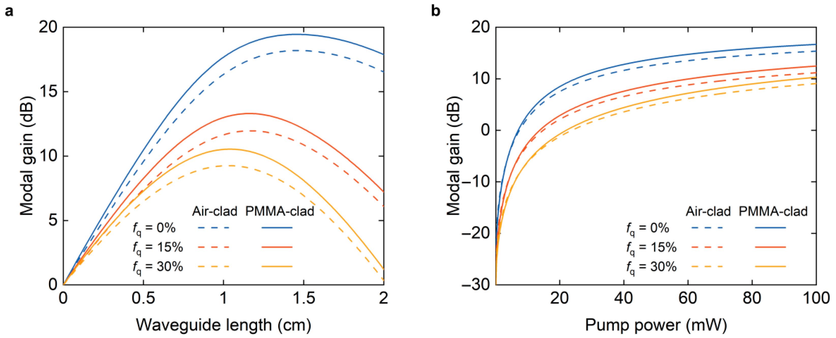
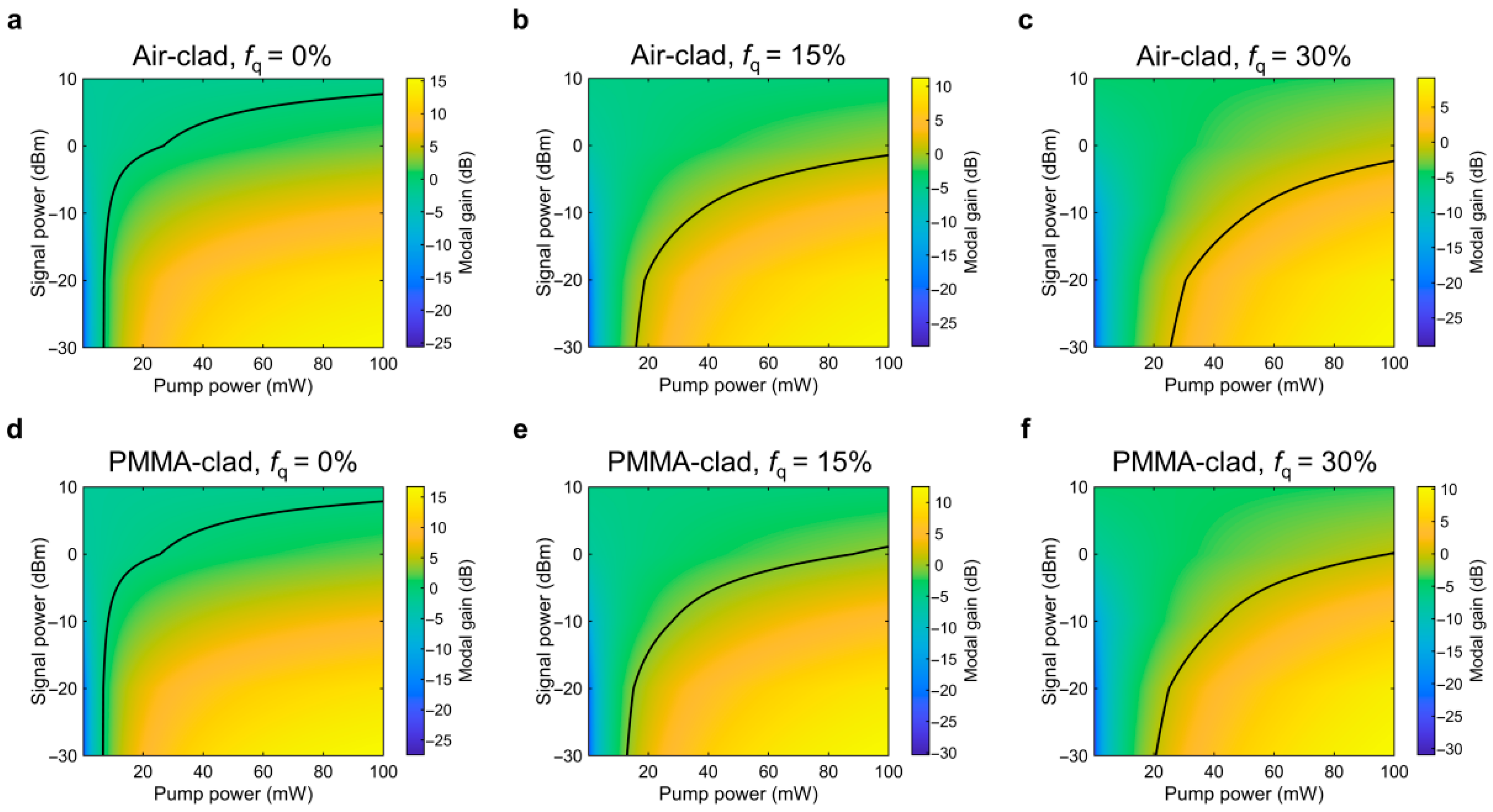
3.2. Numerical Simulation of Optical Amplification

The amplification dynamics in PMMA-clad and air-clad amplifiers with different fractions of quenched ions fq have been elaborately investigated. Modal gain as a function of waveguide length is first simulated for both waveguide amplifiers with different fractions of quenched ions, fq = 0%, 15%, and 30%, as shown in Figure 4a. It can be clearly seen that the PMMA-clad amplifier obtains a higher modal gain than the air-clad amplifier at the same fractions of quenched ions. To be more specific, the PMMA-clad amplifier obtains a maximum modal gain of 19.5 dB, which is higher than that of the air-clad amplifier, at 18.1 dB, when the waveguide length is 1.5 cm in the absence of quenched ions. By further increasing the waveguide length to 2 cm, the modal gain of both amplifiers decreased slightly by about 1.5 dB, which can be attributed to insufficient pump power. In contrast, the maximum modal gains obtained by the PMMA-clad amplifier and air-clad amplifier are 10.6 dB and 9.2 dB, respectively, at the waveguide length of 1 cm for fq = 30%. This indicates that the presence of quenched ions greatly reduces the optical gain owing to their detrimental absorption of the pump and signal power without contributing to the inversion gain. For a fixed waveguide length of 1 cm, the dependence of the modal gain on the pump power at an input signal power of −30 dBm can be seen in Figure 4b. For both amplifiers, the level of modal gain increase becomes slow and tends to saturate when the pump power exceeds 30 mW. It is worth noting that the larger the fractions of quenched erbium ions, the higher the pump power required to obtain net modal gain.
Furthermore, modal gain as a function of the input pump and signal powers under different fractions of quenched erbium ions is calculated for air-clad and PMMA-clad waveguide amplifiers. As shown in Figure 5, the fractions of quenched erbium ions exhibit a significant effect on the modal gain of the waveguide amplifiers. The ‘0’ gain plots in the gain maps are represented by black lines, where the actual loss and gain regions are delimited. The comparison of the modal gains of the air-clad and the PMMA-clad waveguide amplifier in the absence of quenched erbium ions is given in Figure 5a,d. Both amplifiers have the same gain behavior with comparable gain values. According to the variation in the ‘0’ dB plots, the presence of quenched erbium ions significantly reduces the area of the actual gain region, as shown in Figure 5b,e. At the same signal power, to achieve identical modal gain, smaller input pump power is required for the PMMA-clad waveguide amplifier relative to the air-clad waveguide amplifier. Figure 5c,f shows modal gain assuming that 30% of the active erbium ions are rapidly quenched. Both amplifiers exhibit a further reduction in the actual gain area compared to fq = 15%. Moreover, the PMMA-clad waveguide amplifier provides a larger maximum small-signal gain and actual gain area than the air-clad waveguide amplifier. The findings of this investigation reveal the potential contribution of the cladding materials to reducing the counteracting role of quenched erbium ions. Although a portion of input optical power in the PMMA-clad waveguide amplifier is guided outside the active region, leading to a decrease in the detrimental absorption of pump and signal powers by quenched erbium ions, this decrease can be compensated by a more uniform inversion along the entire length of the waveguide amplifier. In addition, the PMMA-clad waveguide amplifier confines a portion of the input pump power in the cladding material, which mitigates the excessive excitation of erbium ions. Thus, the energy transfer upconversion process is alleviated, allowing for higher modal gain.
Figure 6a exhibits modal gain as a function of input signal power at a pump power of 20 dBm. It can be seen that for the same configuration, the higher the fractions of quenched erbium ions, the smaller the modal gain. As the input signal power increases, the modal gain provided by both amplifiers gradually decreases. The reason for this phenomenon may be the depletion of excited-state erbium ions by the stimulated emissions from high power signals. In addition, the PMMA-clad waveguide amplifier has a higher small-signal modal gain than the air-clad waveguide amplifier, while at high power signals the modal gains obtained by both amplifiers are pretty close to each other, taking into account the presence of quenched erbium ions. It is pleasing to note that the PMMA-clad waveguide amplifier maintains a modal gain of over 10 dB at fq = 30%. The derived noise figures at various input pump powers for a forward pumping scheme are shown in Figure 6b. The noise figure of both amplifiers decreases as the pump power increases with different fractions of quenched ions. When the pump power is lower than 13 dBm, with higher fractions of quenched ions for both amplifiers, the noise figures are smaller, and the PMMA-clad waveguide amplifier noise is smaller than the air-clad noise at the same fractions of quenched ions. As a result, increasing the pumping power enables the device to achieve a larger modal gain and lower noise figure.
Based on the above study, we further explore the performance of the PMMA-clad hybrid waveguide amplifier with fractions of quenched ions fq = 30%. The calculated modal gain versus input pump power and waveguide length is given in Figure 7. For a PMMA-clad hybrid waveguide amplifier with an Er concentration of 3 × 1020 cm−3 and Yb concentration of 2.4 × 1021 cm−3, an optimized waveguide length of 1.4 cm can be found that is capable of delivering more than 20 dB of modal gain with a power pump of around 25 dBm. Modal gain is further increased by applying a higher input pump power or reducing propagation losses, but a further increase in waveguide length would not improve the modal gain significantly. This is primarily due to the fact that erbium signal reabsorption is more likely to occur in longer waveguides.
A comparison of recently reported erbium-doped waveguide amplifiers is presented in Table 2. The table compares integrated amplifiers with various material platforms in terms of the active material, active region length, erbium doping concentration, and gain. The proposed hybrid waveguide amplifier presents a strategy for high-efficiency on-chip amplification. This provides an avenue for the development of active devices based on passive SiN photonic platforms.

4. Discussion

The development of high-gain integrated waveguide amplifiers is critical for scaling photonic integrated circuits. We propose an efficient amplification scheme based on a hybrid slot waveguide consisting of SiN waveguides and a thin-film Er-Yb:Al2O3/electron-beam resist. By very carefully engineering the optical mode supported in such a hybrid waveguide, the PMMA-clad hybrid waveguide features higher single-mode conservation than conventional air/SU8-clad hybrid waveguides at 1530 nm. A comprehensive dynamic model of the Er-Yb co-doped amplifier is developed by introducing quenched ions. The results demonstrate that a PMMA-clad hybrid waveguide amplifier exhibits a modal gain of more than 20 dB.
The advantage of this hybrid waveguide based on a silicon nitride photonic platform enables the flexible engineering of the guided mode and the modal overlap between pump and signal beams and the active layer in a hybrid slot structure by changing the cladding material. Compared to conventional air/SU8-clad hybrid waveguides, the PMMA-clad hybrid waveguide features higher single-mode conservation. To better reflect actual conditions, a comprehensive dynamic model of Er-Yb co-doped amplifiers is further established by introducing quenching ions based on our previous research [27]. As expected, the PMMA-clad amplifier obtains a higher modal gain than the air-clad amplifier in the presence of quenched ions, in agreement with the results reported in Ref. [48]. Moreover, it is evident that the increase in the proportion of quenched ions significantly reduces the modal gain, owing to their deleterious absorption of pump and signal powers without facilitating the inversion gain, consistent with the results reported in Ref. [22].
Another advantage stems from the active material nanostructure design, which mitigates the concentration-quenching effect caused by pump depletion and energy transfer upconversion. Recent studies have shown that bidirectional energy cycling between Er ions and Yb ions is the primary factor contributing to pump depletion at high doping concentrations. Specifically, the reverse transfer from Er ions to Yb ions competes with forward sensitization, leading to the nonlinear quenching of red emissions [49]. To suppress energy transfer upconversion, an engineered core-shell nanostructure with an interfacial energy transfer layer was proposed. This strategy reduces losses due to energy transfer upconversion in high-concentration Er-Yb systems by isolating Er ion clusters [50].
In addition, the host material is a key factor affecting the performance of EDWAs. Al2O3 is a promising candidate host material due to its wide transparency window, high thermal conductivity, and excellent mechanical stability. However, the presence of intrinsic and extrinsic point defects in Al2O3 introduces characteristic absorption bands in the visible and even near-infrared regions [51,52,53,54]. These defects introduce parasitic absorption losses, compete with Er ions for pumping energy, and finally affect the gain performance of EDWAs. Although these point defects in Al2O3 trigger a marked challenge to the efficient amplification of EDWAs, using a co-doping strategy with sensitizers (e.g., Yb ions) to improve pump absorption efficiency and mitigate the concentration-quenching effect may be a feasible solution.
Despite the comprehensive theoretical scheme proposed, achieving efficient amplification in SiN-based photonic integrated circuits necessitates trade-offs among optical performance, thermal stability, and fabrication feasibility. Yet, although PMMA is essential in high-gain, low-cost erbium-doped waveguide amplifiers due to low optical losses and the ease of processing, thermal stability shortcomings limit its industrial applications. Exploring alternative cladding materials with enhanced thermal and environmental resilience while mitigating the potential negative impact on optical performance (e.g., by engineering composite cladding interfaces, exploring graded indices, or utilizing lower-index stable polymers) is a critical and valuable direction for future research in real-world applications. In addition, it could allow for the co-doping of other rare-earth ions such as neodymium and thulium, thereby providing optical gain in other wavelength regions.

5. Conclusions

In conclusion, we have theoretically proposed PMMA-clad hybrid waveguide amplifiers based on a SiN photonic platform, in which one can flexibly engineer the guided mode and the modal overlap between the pump and signal beams and active layer in a hybrid slot structure. An accurate and comprehensive dynamic model of an Er-Yb co-doped amplifier considering quenched ions is developed. A modal gain of above 20 dB can be achieved at 1530 nm within a 1.4 cm hybrid slot waveguide for an Er concentration of 3 × 1020 cm−3 and a Yb concentration of 2.4 × 1021 cm−3 with fractions of quenched ions fq = 30%. This work offers a strategy for designing high-gain waveguide amplifiers with a simple fabrication process and unveils the versatility of SiN-based photonic integrated circuits. It will enrich the building blocks in active platforms and pave the way for the development of on-chip high-efficiency amplification.

Author Contributions

Conceptualization, Z.D.; methodology, G.S.; software, Z.D.; validation, Y.Z.; formal analysis, Y.W.; investigation, Z.D.; writing—original draft preparation, Z.D.; writing—review and editing, L.D., L.T. and Y.L. All authors have read and agreed to the published version of the manuscript.

Funding

This work was supported by the National Key Research and Development Program of China (2020YFB1805801) and the National Natural Science Foundation of China (12034010).

Institutional Review Board Statement

Not applicable.

Informed Consent Statement

Not applicable.

Data Availability Statement

The data presented in this study are available on request from the corresponding author.

Conflicts of Interest

The authors declare no conflicts of interest.

References

  1. Poole, S.; Payne, D.; Mears, R.; Fermann, M.; Laming, R. Fabrication and characterization of low-loss optical fibers containing rare-earth ions. J. Light. Technol. 1986, 4, 870–876. [Google Scholar] [CrossRef]
  2. Bradley, J.D.B.; Pollnau, M. Erbium-doped integrated waveguide amplifiers and laser. Laser Photon. Rev. 2011, 5, 368–403. [Google Scholar] [CrossRef]
  3. Zhang, H.; He, Y.; Zhu, S.; Zhou, X.; Zhang, L. Atomic-layer engineered erbium-doped waveguide amplifier with a 14.4 dB net gain. ACS Photonics 2025, 12, 674–683. [Google Scholar] [CrossRef]
  4. Zhou, J.; Liang, Y.; Liu, Z.; Chu, W.; Zhang, H.; Yin, D.; Fang, Z.; Wu, R.; Zhang, J.; Chen, W.; et al. On-chip integrated waveguide amplifiers on erbium-doped thin-film lithium niobate on insulator. Laser Photon. Rev. 2021, 15, 2100030. [Google Scholar] [CrossRef]
  5. Wang, C.; Song, J.; Ao, Z.; Yang, S.; Li, Y.; Li, X.; Zhu, N.; Chen, Q.; Li, Z. High-gain waveguide amplifiers in Ge25Sb10S65 photonics heterogeneous integration with erbium-doped Al2O3 thin films. Laser Photon. Rev. 2023, 18, 2300893. [Google Scholar] [CrossRef]
  6. Tao, S.; Song, H.; Zhao, D.; Yang, Y.; Wang, S.; Yan, J.; Wei, J.; Wang, X.; Qin, G.; Wang, F. Strip loaded waveguide amplifiers based on erbium-doped nanocomposites with 17 dB internal net gain. Opt. Express 2024, 32, 7931–7939. [Google Scholar] [CrossRef] [PubMed]
  7. Rönn, J.; Zhang, W.; Autere, A.; Leroux, X.; Pakarinen, L.; Alonso-Ramos, C.; Säynätjoki, A.; Lipsanen, H.; Vivien, L.; Cassan, E.; et al. Ultra-high on-chip optical gain in erbium-based hybrid slot waveguides. Nat. Commun. 2019, 10, 432. [Google Scholar] [CrossRef] [PubMed]
  8. Chen, Z.; Wan, L.; Gao, S.; Zhu, K.; Zhang, M.; Li, Y.; Huang, X.; Li, Z. On-chip waveguide amplifiers for multi-band optical communications: A review and challenge. J. Light. Technol. 2022, 40, 3364–3373. [Google Scholar] [CrossRef]
  9. Zhu, D.; Shao, L.; Yu, M.; Cheng, R.; Desiatov, B.; Xin, C.; Hu, Y.; Holzgrafe, J.; Ghosh, S.; Shams-Ansari, A.; et al. Integrated photonics on thin-film lithium niobate. Adv. Opt. Photonics 2021, 13, 242–352. [Google Scholar] [CrossRef]
  10. Zhang, Z.; Li, S.; Gao, R.; Zhang, H.; Lin, J.; Fang, Z.; Wu, R.; Wang, M.; Wang, Z.; Hang, Y.; et al. Erbium-ytterbium codoped thin-film lithium niobate integrated waveguide amplifier with a 27 dB internal net gain. Opt. Lett. 2023, 48, 4344–4347. [Google Scholar] [CrossRef] [PubMed]
  11. Zhang, X.; Yan, J.; Wang, C.; Sun, T.; Cao, Z.; Xu, C.; Qin, G.; Wang, F.; Zhang, D. Design of a few-mode erbium-ytterbium co-doped polymer optical waveguide amplifier with low differential modal gain. J. Light. Technol. 2021, 39, 3201–3216. [Google Scholar] [CrossRef]
  12. Xu, X.; Inaba, T.; Tsuchizawa, T.; Ishizawa, A.; Sanada, H.; Tawara, T.; Omi, H.; Oguri, K.; Gotoh, H. Low-loss erbium-incorporated rare-earth oxide waveguides on Si with bound states in the continuum and the large optical signal enhancement in them. Opt. Express 2021, 29, 41132–41143. [Google Scholar] [CrossRef]
  13. Zhang, Z.; Liu, R.; Wang, W.; Yan, K.; Yang, Z.; Song, M.; Wu, D.; Xu, P.; Wang, X.; Wang, R. On-chip Er-doped Ta2O5 waveguide amplifiers with a high internal net gain. Opt. Lett. 2023, 48, 5799–5802. [Google Scholar] [CrossRef] [PubMed]
  14. Liang, D.; Bowers, J.E. Recent progress in heterogeneous III-V-onsilicon photonic integration. Light Adv. Manuf. 2021, 2, 59–83. [Google Scholar] [CrossRef]
  15. Xiang, C.; Jin, W.; Bowers, J.E. Silicon nitride passive and active photonic integrated circuits: Trends and prospects. Photonics Res. 2022, 10, 82–96. [Google Scholar] [CrossRef]
  16. Li, Z.; Wang, R.N.; Lihachev, G.; Zhang, J.; Tan, Z.; Churaev, M.; Kuznetsov, N.; Siddharth, A.; Bereyhi, M.J.; Riemensberger, J.; et al. High density lithium niobate photonic integrated circuits. Nat. Commun. 2023, 14, 4856. [Google Scholar] [CrossRef] [PubMed]
  17. Levy, J.S.; Gondarenko, A.; Foster, M.A.; Turner-Foster, A.C.; Gaeta, A.L.; Lipson, M. CMOS-compatible multiple-wavelength oscillator for on-chip optical interconnects. Nat. Photonics 2009, 4, 37–40. [Google Scholar] [CrossRef]
  18. Moss, D.J.; Morandotti, R.; Gaeta, A.L.; Lipson, M. New CMOS-compatible platforms based on silicon nitride and Hydex for nonlinear optics. Nat. Photonics 2013, 7, 597–607. [Google Scholar] [CrossRef]
  19. Liu, J.; Huang, G.; Wang, R.N.; He, J.; Raja, A.S.; Liu, T.; Engelsen, N.J.; Kippenberg, T.J. High-yield, wafer-scale fabrication of ultralow-loss, dispersion-engineered silicon nitride photonic circuits. Nat. Commun. 2021, 12, 2236. [Google Scholar] [CrossRef] [PubMed]
  20. Purnawirman; Sun, J.; Adam, T.N.; Leake, G.; Leake, G.; Coolbaugh, D.; Bradley, J.D.B.; Hosseini, E.S.; Watts, M.R. C-and L-band erbium-doped waveguide lasers with wafer-scale silicon nitride cavities. Opt. Lett. 2013, 38, 1760–1762. [Google Scholar] [CrossRef] [PubMed]
  21. Mu, J.; Dijkstra, M.; Korterik, J.; Offerhaus, H.; García-Blanco, S.M. High-gain waveguide amplifiers in Si3N4 technology via double-layer monolithic integration. Photonics Res. 2020, 8, 1634–1641. [Google Scholar] [CrossRef]
  22. Frankis, H.C.; Mbonde, H.M.; Bonneville, D.B.; Zhang, C.; Mateman, R.; Leinse, A.; Bradley, J.D.B. Erbium-doped TeO2-coated Si3N4 waveguide amplifiers with 5 dB net gain. Photonics Res. 2020, 8, 127–134. [Google Scholar] [CrossRef]
  23. Rönn, J.; Zhang, J.; Zhang, W.; Tu, Z.; Matikainen, A.; Leroux, X.; Durán-Valdeiglesias, E.; Vulliet, N.; Boeuf, F.; Alonso-Ramos, C. Erbium-doped hybrid waveguide amplifiers with net optical gain on a fully industrial 300 mm silicon nitride photonic platform. Opt. Express 2020, 28, 27919–27926. [Google Scholar] [CrossRef] [PubMed]
  24. Chrysostomidis, T.; Roumpos, I.; Fotiadis, K.; Mu, J.; Manolis, A.; Vagionas, C.; Dijkstra, M.; Blanco, S.G.; Alexoudi, T.; Vyrsokinos, K. 480 Gbps WDM transmission through an Al2O3:Er3+ waveguide amplifier. J. Light. Technol. 2022, 40, 735–743. [Google Scholar] [CrossRef]
  25. Vagionas, C.; Tsakyridis, A.; Chrysostomidis, T.; Roumpos, I.; Fotiadis, K.; Manolis, A.; Mu, J.; Dijkstra, M.; Blanco, S.G.; Oldenbeuving, R.M.; et al. Lossless 1×4 silicon photonic ROADM based on a monolithic integrated erbium doped waveguide amplifier on a Si3N4 Platform. J. Light. Technol. 2022, 40, 1718–1725. [Google Scholar] [CrossRef]
  26. Riemensberger, J.; Kuznetsov, N.; Liu, J.; He, J.; Wang, R.N.; Kippenberg, T.J. A photonic integrated continuous-travelling-wave parametric amplifier. Nature 2022, 612, 56–61. [Google Scholar] [CrossRef] [PubMed]
  27. Dong, Z.; Zhao, Y.; Wang, Y.; Wei, W.; Ding, L.; Tang, L.; Li, Y. Gain optimization of an erbium-ytterbium co-doped amplifier via a Si3N4 photonic platform. Opt. Express 2023, 31, 35419–35430. [Google Scholar] [CrossRef] [PubMed]
  28. Crawford, J.H., Jr. Defects and defect processes in ionic oxides: Where do we stand today? Nucl. Instrum. Meth. B. 1984, 1, 159–165. [Google Scholar] [CrossRef]
  29. Evans, B.D.; Pogatshnik, G.J.; Chen, Y. Optical properties of lattice defects in α-Al2O3. Nucl. Instrum. Meth. B. 1994, 91, 258–262. [Google Scholar] [CrossRef]
  30. Xu, X.; Fili, V.; Szuba, W.; Hiraishi, M.; Inaba, T.; Tawara, T.; Omi, H.; Gotoh, H. Epitaxial single-crystal rare-earth oxide in horizontal slot waveguide for silicon-based integrated active photonic devices. Optics. Express 2020, 28, 14448–14460. [Google Scholar] [CrossRef] [PubMed]
  31. Kempf, E.; Romeo, P.R.; Gassenq, A.; Taute, A.; Chantraine, P.; John, J.; Belarouci, A.; Monfray, S.; Boeuf, F.; Charette, P.G. SiN half-etch horizontal slot waveguides for integrated photonics: Numerical modeling, fabrication, and characterization of passive components. Opt. Express 2022, 30, 4202–4214. [Google Scholar] [CrossRef] [PubMed]
  32. Wei, N.; Li, X.; He, J.; Fan, Y.; Dan, Y.; Wang, J. Design of an optical slot waveguide amplifier based on Er3+-doped tellurite glass. Chin. Opt. Lett. 2023, 21, 011404. [Google Scholar] [CrossRef]
  33. Kita, D.M.; Michon, J.; Johnson, S.G.; Hu, J. Are slot and sub-wavelength grating waveguides better than strip waveguides for sensing? Optica 2018, 5, 1046–1054. [Google Scholar] [CrossRef]
  34. Sultanova, N.; Kasarova, S.; Nikolov, I. Dispersion properties of optical polymers. Acta Phys. Pol. A 2009, 116, 585–587. [Google Scholar] [CrossRef]
  35. Bonneville, D.B.; Frankis, H.C.; Wang, R.; Bradley, J.D.B. Erbium-ytterbium co-doped aluminium oxide waveguide amplifiers fabricated by reactive co-sputtering and wet chemical etching. Opt. Express 2020, 28, 30130–30140. [Google Scholar] [CrossRef] [PubMed]
  36. Luke, K.; Okawachi, Y.; Lamont, M.R.E.; Gaeta, A.L.; Lipson, M. Broadband mid-infrared frequency comb generation in a Si3N4 microresonator. Opt. Lett. 2015, 40, 4823–4826. [Google Scholar] [CrossRef] [PubMed]
  37. Tan, C.Z. Determination of refractive index of silica glass for infrared wavelengths by IR spectroscopy. J. Non-Cryst. Solids 1998, 223, 158–163. [Google Scholar] [CrossRef]
  38. Agazzi, L.; Worhoff, K.; Pollnau, M. Energy-transfer-upconversion models, their applicability and breakdown in the presence of spectroscopically distinct ion classes: A case study in amorphous Al2O3:Er3+. J. Phys. Chem. C 2013, 117, 6759–6776. [Google Scholar] [CrossRef]
  39. Zhou, P.; Wang, S.; Wang, X.; He, Y.; Zhou, Z.; Zhou, L.; Wu, K. High-gain erbium silicate waveguide amplifier and a low-threshold, high-efficiency laser. Opt. Express 2018, 26, 16689–16707. [Google Scholar] [CrossRef] [PubMed]
  40. Zhang, M.; Zhang, W.; Wang, F.; Zhao, D.; Qu, C.; Wang, X.; Yi, Y.; Cassan, E.; Zhang, D. High-gain polymer optical waveguide amplifiers based on core-shell NaYF4/NaLuF4: Yb3+, Er3+ NPs-PMMA covalent-linking nanocomposites. Sci. Rep. 2016, 6, 36729. [Google Scholar] [CrossRef] [PubMed]
  41. Liu, Y.; Qiu, Z.; Ji, X.; Lukashchuk, A.; He, J.; Riemensberger, J.; Hafermann, M.; Wang, R.N.; Liu, J.; Ronning, C.; et al. A photonic integrated circuit-based erbium-doped amplifier. Science 2022, 376, 1309–1313. [Google Scholar] [CrossRef] [PubMed]
  42. Wang, B.; Zhou, P.; Wang, X.; He, Y. A low-fabrication-temperature, high-gain chip-scale waveguide amplifier. Sci. China Inform. Sci. 2022, 65, 162405. [Google Scholar] [CrossRef]
  43. Tao, S.; Yan, J.; Song, H.; Wei, J.; Fu, Y.; Zhao, D.; Wang, F.; Zhang, D. Modeling and simulation of erbium-ytterbium co-doped optical waveguide amplifiers with dual-wavelength pumping at 980 nm and 1480 nm. J. Phy. D. Appl. Phys. 2023, 56, 344003. [Google Scholar] [CrossRef]
  44. Zhou, C.; He, X.; Xiao, M.; Ma, D.; Chen, W.; Zhou, Z. Design of an on-chip wavelength conversion device assisted by an erbium-ytterbium co-doped waveguide amplifier. Front. Optoelectron. 2024, 17, 16. [Google Scholar] [CrossRef] [PubMed]
  45. He, X.; Ma, D.; Zhou, C.; Xiao, M.; Chen, W.; Zhou, Z. On-chip integrated few-mode erbium–ytterbium co-doped waveguide amplifiers. Photonics Res. 2024, 12, 1067–1077. [Google Scholar] [CrossRef]
  46. Zhang, M.; Hu, G.; Zhang, S.; Gao, D.; Sun, Y.; Wang, F. Gain characteristics of the hybrid slot waveguide amplifiers integrated with NaYF4:Er3+ NPs-PMMA covalently linked nanocomposites. RSC Adv. 2020, 10, 11148–11155. [Google Scholar] [CrossRef] [PubMed]
  47. Cai, M.; Wu, K.; Xiang, J.; Xiao, Z.; Li, T.; Li, C.; Chen, J. Erbium-doped lithium niobate thin film waveguide amplifier with 16 dB internal net gain. IEEE J. Sel. Top. Quantum Electron. 2022, 28, 1–8. [Google Scholar] [CrossRef]
  48. Liang, Y.; Zhou, J.; Liu, Z.; Zhang, H.; Fang, Z.; Zhou, Y.; Yin, D.; Lin, J.; Yu, J.; Wu, R.; et al. A high-gain cladded waveguide amplifier on erbium doped thin-film lithium niobate fabricated using photolithography assisted chemo-mechanical etching. Nanophotonics 2022, 11, 1033–1040. [Google Scholar] [CrossRef] [PubMed]
  49. Shi, Y.; Wu, H.; Wu, H.; Zhang, L.; Pan, G.H.; Luo, Y.; Hao, Z.; Zhang, J. The important round-trip energy transfer for excitation of the red emission in the Er3+/Yb3+ System. J. Phys. Chem. Lett. 2025, 16, 1336–1342. [Google Scholar] [CrossRef] [PubMed]
  50. Huang, J.; Tu, L.; Huang, H.; Wei, H.; Zhang, Q.; Zhou, B. Manipulating energy migration in nanoparticles toward tunable photochromic upconversion. Nat. Commun. 2024, 15, 10890. [Google Scholar] [CrossRef] [PubMed]
  51. Cooke, D.W.; Roberts, H.E.; Alexander, C., Jr. Thermoluminescence and emission spectra of uv-grade Al2O3 from 90 to 500 K. J. Appl. Phys. 1978, 49, 3451–3457. [Google Scholar] [CrossRef]
  52. Kotomin, E.A.; Popov, A.I. Radiation-induced point defects in simple oxides. Nucl. Instrum. Meth. B. 1998, 141, 1–15. [Google Scholar] [CrossRef]
  53. Rani, G.; Sahare, P.D. Effect of phase transitions on thermoluminescence characteristics of nanocrystalline alumina. Nucl. Instrum. Meth. B. 2013, 311, 71–77. [Google Scholar] [CrossRef]
  54. Ananchenko, D.V.; Nikiforov, S.V.; Kuzovkov, V.N.; Popov, A.I.; Ramazanova, G.R.; Batalov, R.I.; Bayazitov, R.M.; Novikov, H.A. Radiation-induced defects in sapphire single crystals irradiated by a pulsed ion beam. Nucl. Instrum. Meth. B. 2020, 466, 1–7. [Google Scholar] [CrossRef]
Figure 1. Design of the hybrid slot waveguide amplifier. (a) Schematic illustration of the hybrid slot waveguide amplifier. The dashed box displays the Er-Yb co-doped energy-level transition diagram optically excited by a 980 nm pump. (b) Simplified cross section at the central axis of the hybrid slot waveguide structure, and description of the parameters. (c) Refractive index and group refractive index profiles of the hybrid slot waveguide and cladding materials at λ = 400~1600 nm. (d) Dispersion evolution of the fundamental transverse electric mode with the same wavelength range. (e) The simulated fundamental transverse modes (TE/TMs) for the waveguide at λ = 980 nm and λ = 1530 nm.
Photonics 12 00718 g001
Figure 2. Optimizations of the waveguide with the overlap confinement factors Γ and the effective mode areas Aeff for the pump beam at 980 nm (red curves) and the signal beam at 1530 nm (blue curves). (a) Γ and Aeff of the TE-mode dependence on Wslot in the range from 1 nm to 300 nm (HSiN = 500 nm, WSiN = 500 nm). (b) Γ and Aeff of the TE mode as a function of HSiN in the range from 100 nm to 500 nm (Wslot = 150 nm, WSiN = 500 nm). (c) Γ and Aeff of the TE mode as a function of WSiN in the range from 100 nm to 500 nm (Wslot = 150 nm, HSiN = 400 nm).
Photonics 12 00718 g002
Figure 3. The confinement factor versus upper cladding refractive index value from 1.0 to 1.6 with Wslot = 150 nm, HSiN = 400 nm, and WSiN = 300 nm at λ = 980 nm (a) and λ = 1530 nm (b). The insets show the TE-mode profiles with air, PMMA, and SU-8 as the upper cladding materials of the hybrid slot waveguide for the corresponding cross section. The black arrows indicate the Γ corresponding to the upper cladding.
Photonics 12 00718 g003
Figure 4. Optical amplification characterization for both waveguide amplifiers. (a) Dependence of modal gain on waveguide length with different fractions of quenched ions. (b) Calculation of modal gain as a function of pump power for the 1 cm long hybrid slot waveguide.
Photonics 12 00718 g004
Figure 5. Calculated modal gain for air-clad (ac) and PMMA-clad (df) waveguide amplifiers as functions of input signal and pump power in a 1 cm long hybrid slot waveguide.
Photonics 12 00718 g005
Figure 6. Modal gain and noise figure performance for both waveguide amplifiers. (a) Modal gain versus input signal power with a pump power of 20 dBm. (b) Noise figure dependence on pump power at an input signal of −30 dBm.
Photonics 12 00718 g006
Figure 7. Calculated modal gain under various input pump powers at 980 nm and different waveguide lengths for an input signal of −30 dBm at 1530 nm. The star marker denotes the optimized waveguide length and pump power in the PMMA-clad hybrid waveguide amplifier.
Photonics 12 00718 g007
Table 1. Parameters of an Er-Yb-based hybrid slot waveguide.
ParameterSymbolValue
Er concentrationNEr3 × 1020 cm−3
Yb concentrationNYb2.4 × 1021 cm−3
Lifetime of state 4I13/2τ215 ms
Lifetime of state 4I11/2τ320.1 ms
Lifetime of state 4I9/2τ431 μs
Lifetime of state 2F5/2 τ 21 Yb 2 ms
Lifetime of quenched ionsτq1 μs
Er pump absorption cross sectionσ13p2.58 × 10−21 cm2
Er signal emission cross sectionσ21s9.83 × 10−21 cm2
Er signal absorption cross sectionσ12s8.95 × 10−21 cm2
Yb pump emission cross section σ 21 p Yb 1.2 × 10⁻²⁰ cm2
Yb pump absorption cross section σ 12 p Yb 1.2 × 10⁻²⁰ cm2
ASE emission cross sectionσ21,ASE4 × 10−21 cm2
ASE absorption cross sectionσ12,ASE6 × 10−21 cm2
First order CUC coefficientC244.1 × 10−17 cm3s−1
Second order CUC coefficientC354.1 × 10−17 cm3s−1
Cross-relaxation coefficientC143.4 × 10−16 cm3s−1
Fraction of quenched ionsfq0, 15%, 30%
Pump propagation lossα0p2.3 dB/cm
Signal propagation lossα0s0.6 dB/cm
Table 2. Comparison with recently reported erbium-doped waveguide amplifiers.
Waveguide
/Active
Material
Active
Region Length
(cm)
Erbium
Concentration
(cm−3)
Gain
(dB)
MethodReference
SiN/Er:Al2O30.124.9 × 10211.98Exp.[7]
SiN/Er:TeO26.72.5 × 10205Exp.[22]
SiN/Er:Al2O30.163.88 × 10213.13Exp.[23]
Si/Er:Polymer1.51.3 × 10215.78Theo.[46]
Er:LiNO33.61.9 × 102018Exp.[4]
Er:LiNO32.587.2 × 101916Exp.[47]
Si/Er:TeO242.2 × 102015.21Theo.[32]
Er:Yb co-doped11.644 × 102118.77Theo.[44]
HSQ/Er:Al2O39.312.5 × 102014.4Exp.[3]
SiN/Er:Al2O31.43 × 102020Theo.This work
Disclaimer/Publisher’s Note: The statements, opinions and data contained in all publications are solely those of the individual author(s) and contributor(s) and not of MDPI and/or the editor(s). MDPI and/or the editor(s) disclaim responsibility for any injury to people or property resulting from any ideas, methods, instructions or products referred to in the content.

