1. Introduction
With the development of mobile communications, the spectrum resource of traditional RF has become increasingly strained, prompting a shift in the research focus towards higher electromagnetic frequency domains [
1,
2]. The unlicensed, ultra-large-bandwidth Optical Wireless Communication (OWC) has become one of alternative solutions to the crisis. Optical Camera Communication (OCC), as an emerging research direction in this field, has been incorporated into the Visible Light Communication branch of the OWC standard: IEEE 802.15.7-2018 [
3]. Recent studies have demonstrated the significant application potentials of OCC across multiple domains including underwater communication [
4,
5], vehicular networks [
6], Internet of Things [
7], and indoor positioning [
8].
The OCC system equip LEDs as the emitter and various image sensors as the receiver, among which the Rolling-Shutter CMOS image sensor (RS-CMOS) stands out for its cost effectiveness, and the derived branch technology is known as Rolling-Shutter Optical Camera Communication (RS-OCC) [
9]. RS-OCC takes the advantage of the rolling-shutter exposure mechanism, enabling the signal-sampling frequency at the receiver to substantially exceed the frame rate. Compared to the global-shutter CMOS image sensor, RS-CMOS offers both an economic advantage and a higher communication rate, with a theoretical throughput ranging from 100 bps to 100 Kbps [
10,
11]. The widespread equipment of RS-CMOS in mainstream mobile devices, including smartphones and tablets, provides a base of potential users to RS-OCC, underscoring the importance of continued research in this field.
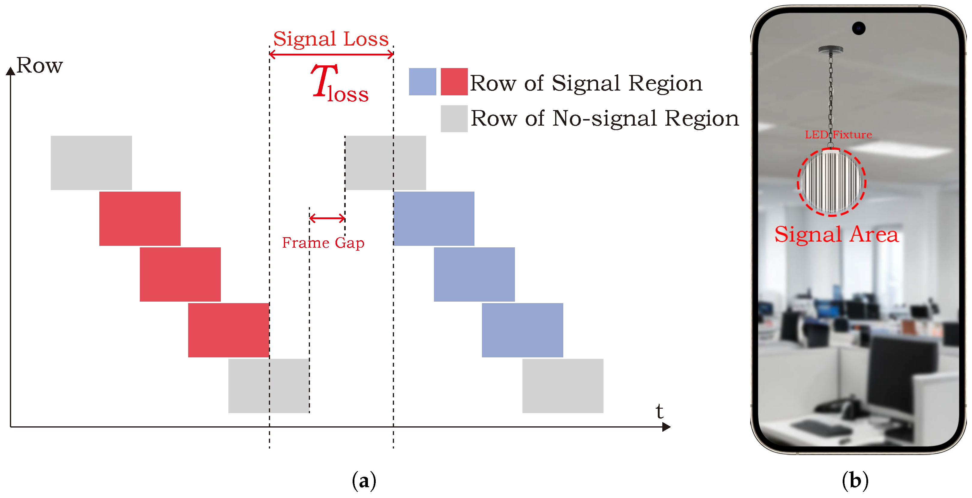
However, RS-OCC faces a challenge of signal loss, manifested as periodic sampling interruptions. This issue stems from two factors: the first factor is the frame-to-frame time gap, preventing signal sampling during this gap. The second factor is a limited signal region. Experimental measurements revealed that the signal region illuminated by the LED covered only 7% of the CMOS pixel array under typical background light and at a communication distance of 3 m, and there was a symbol loss rate of 93.7%where.
Existing mitigation approaches employ various compensation strategies, such as data retransmission [
9,
12], error correction codes [
13,
14], and periodic matching [
15]. Danakis et al. [
9] pioneered the use of RS-CMOS to enhance OCC sampling frequency, employing a simple compensation method. This method sends each data packet twice to enable the receiver to reconstruct the complete packet. Rollinglight [
13] is a low-rate yet robust method extending the bit period to exceed half of the frame period, then performing parity checking to recover lost bits. Nguyen et al. [
14,
16] proposed distributing the bits during each frame gap across different Hamming blocks, then performing error correction on each Hamming block to recover all lost bits. The basic idea of IoTorch [
12] is similar to that of Danakis et al. [
9], ensuring reliable transmission through retransmission. But IoTorch focuses on the periodicity of signal loss and designed a minimum repetition mechanism. These methods usually only consider the factor of the frame gap, and their communication distances are relatively short. In addition, these methods significantly increase the amount of redundant information and lower the net communication rate. To compensate for the rate, researchers have also implemented multiple channels employing Spatial Division Multiplexing by LED arrays [
17,
18], and employed advanced modulation schemes such as Color-Shift Keying (CSK) [
19,
20] and Orthogonal Frequency Division Multiplexing (OFDM) [
21,
22]. These improvements somewhat alleviate signal loss but inevitably increase the decoding latency of the receiver.
The paper focuses on CMOS exposure timing rather than the conventional method of the OCC data frame to address signal loss, and the proposed method requires the capability to precisely control the CMOS exposure timing. However, the parameter heterogeneity between OCC and CMOS presents a significant challenge. The paper establishes a relationship between the OCC sampling parameters and CMOS exposure parameters to identify the critical optimization parameters. Furthermore, the control of exposure timing involves operations at a hardware level. However, the existing experimental platform relies on Android or Windows, and their API demonstrates limited granularity in CMOS parameter control. To address this limitation, the paper implements a experimental platform through a open-source hardware and OS to achieve precise control. The following are the contributions of the paper:
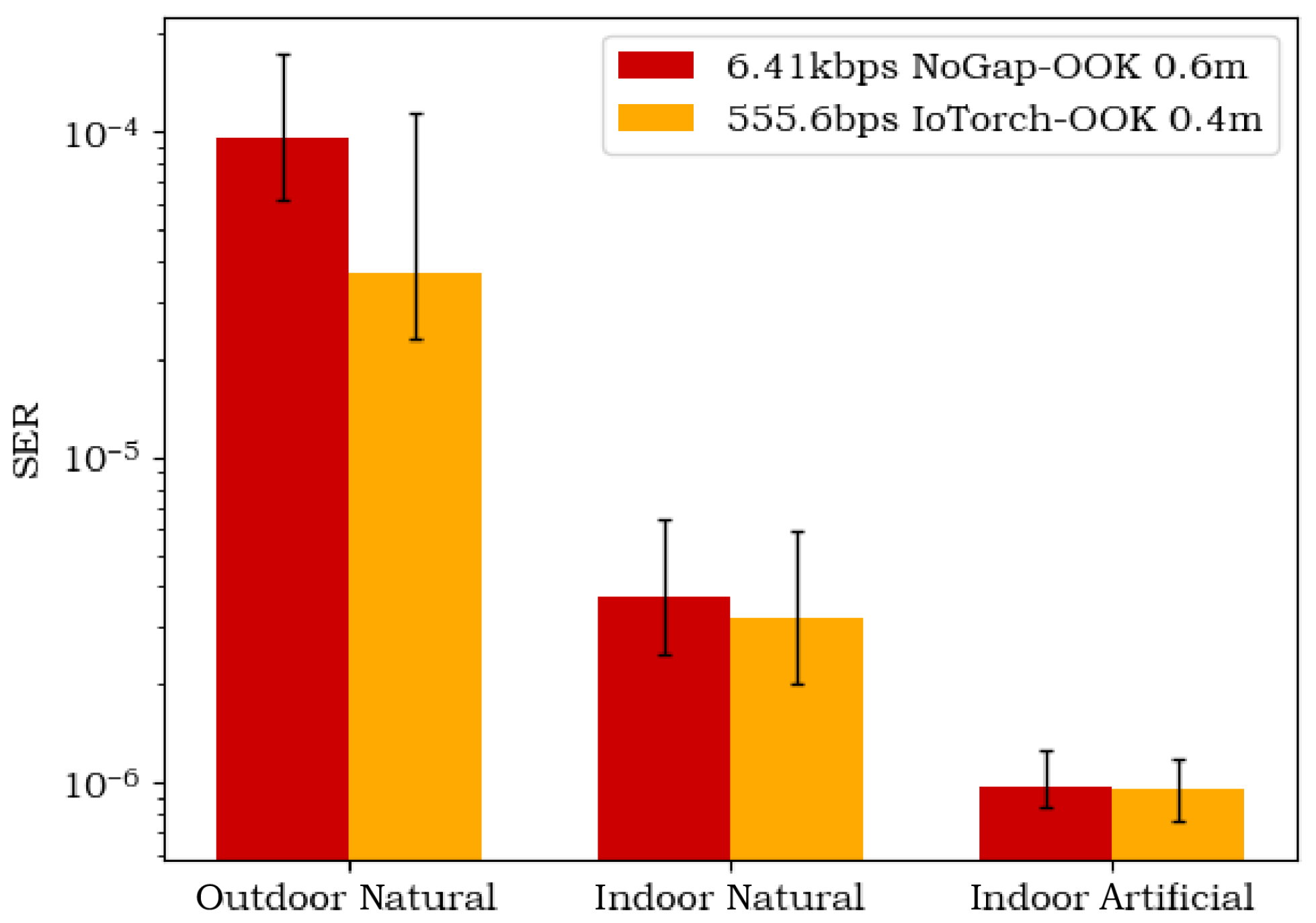
NoGap-RS proposes a gapless signal sampling method for high-rate, low-cost RS-OCC, which addresses the issue of signal loss from a theoretical perspective to extend the application scenarios of RS-OCC. It can work under background light and at a communication distance of 3 m, which is about 5 times better than the baseline [
12].
NoGap-RS is compatible with most modulation schemes, and when used with the On–Off Keying (OOK) modulation under SER of
, it can achieve a communication rate of 6.41 Kbps, which is about 10 times better than the baseline [
12].
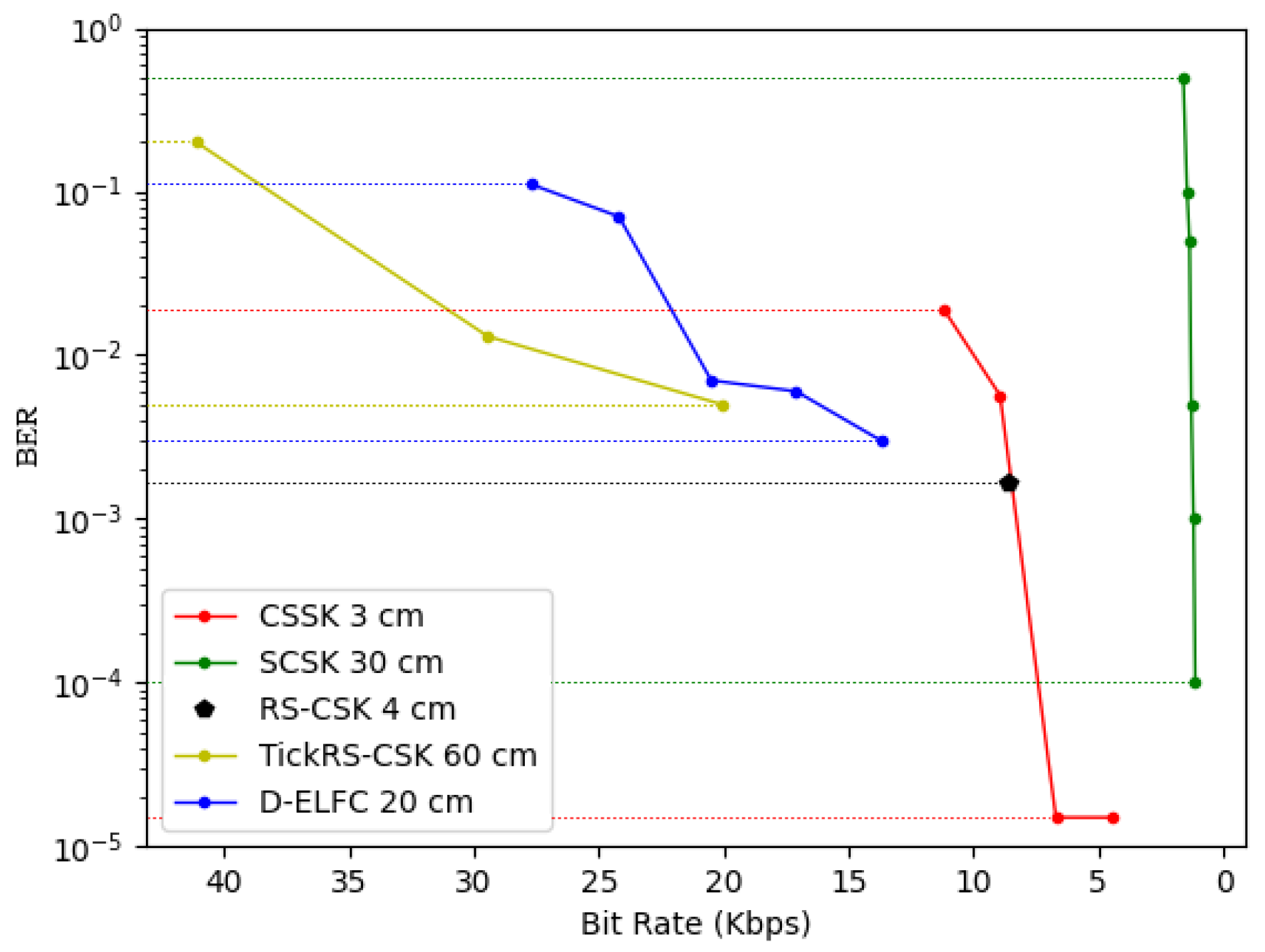
TickRS further proposes a time slot division method, addressing the overlap that occurs during consecutive-row exposures to further enhance the communication rate. TickRS-CSK, an OCC system based on TickRS and Color-Shift Key, can achieve a 48.52% improvement in bit rate compared to baseline systems, along with an extended communication range from 0.2 m to 3.6 m, representing a 3.4 m increase, while maintaining a bit error rate (BER) of 4.36%.
The following is the arrangement of sections in the paper.
Section 2 briefly introduces the basic concepts of the RS-CMOS exposure and RS-OCC, and analyzes in detail two factors that lead to signal loss.
Section 3 introduces NoGap-RS, a gapless signal sampling method, to address signal loss.
Section 4 introduces TickRS, a time slot division method based on NoGap-RS, to improve the symbol rate.
Section 5 designs TickRS-CSK, a complete RS-OCC process.
Section 6 implements an experimental platform of NoGap-RS and TickRS-CSK to evaluate them.
3. NoGap-RS: A No-Gap Sampling Method for RS-OCC
The goal of NoGap-RS is to ensure that the consecutive-frame exposures in the signal region are sufficiently close in time, i.e., , to achieve gapless signal sampling to address signal loss. The approach of NoGap-RS is to precisely control by adjusting various parameters of CMOS.
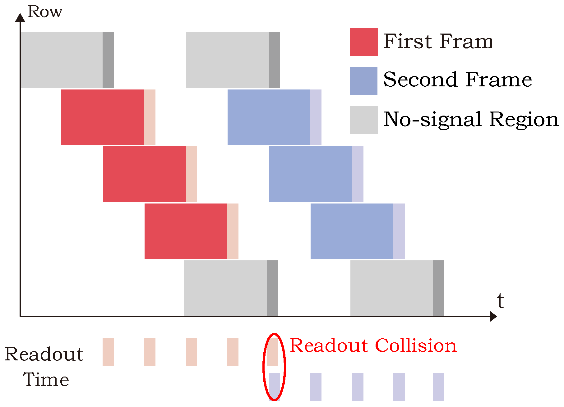
3.1. Read Collision Elimination
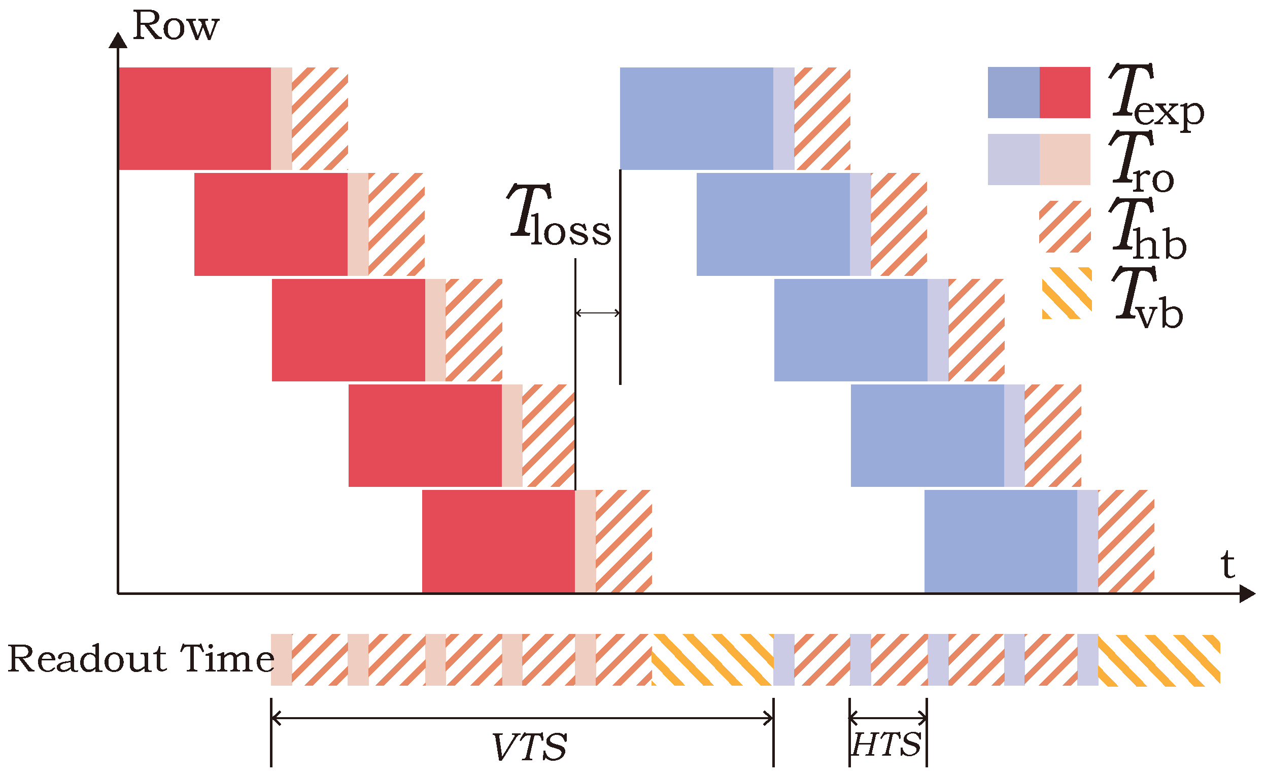
Before controlling
, possible readout collisions should be eliminated. As shown in
Figure 4, the readout collision refers to the readouts of two frames overlapping in time. Reducing
will significantly increase the probability of readout collisions, as CMOS needs to read out all rows under default settings, and the unnecessary non-signal region will occupy a large amount of the readout time. The method of eliminating readout collisions in NoGap-RS is to use exposure window, a configuration of CMOS, which strictly limits the exposure operation to a preset window region. NoGap-RS sets the exposure window to the signal region, thereby stopping the exposure and readout of the non-signal region, effectively eliminating readout collisions.
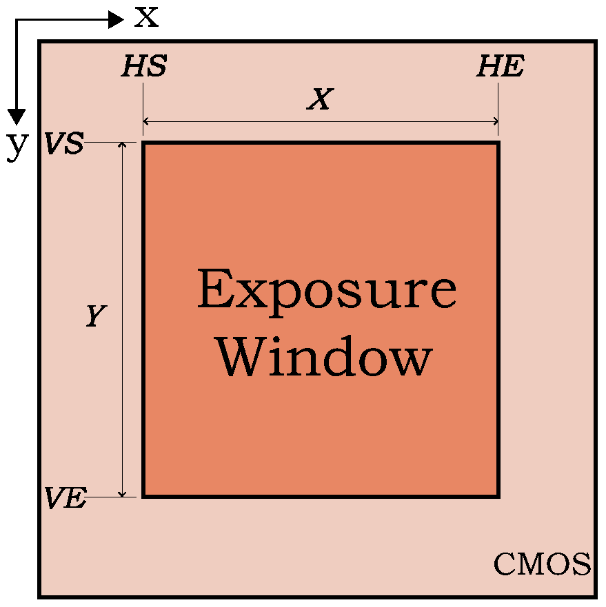
As shown in
Figure 5, the exposure window is a rectangular region of a CMOS pixel array, and its position and size are determined by four parameters:
(horizontal start coordinate),
(vertical start coordinate),
(horizontal end coordinate), and
(vertical end coordinate).
represents the coordinates of the first vertex of the window, while
represents the coordinates of the diagonal vertex. Therefore, the number of rows of the window is
and the number of columns is
Additionally, there is a minimum size constraint in the hardware on the exposure window, and the signal region will be smaller than the minimum exposure window under long-distance communication, resulting in some parts of the non-signal region participating in readout. In this case, should be minimized as much as possible while avoiding readout collisions.
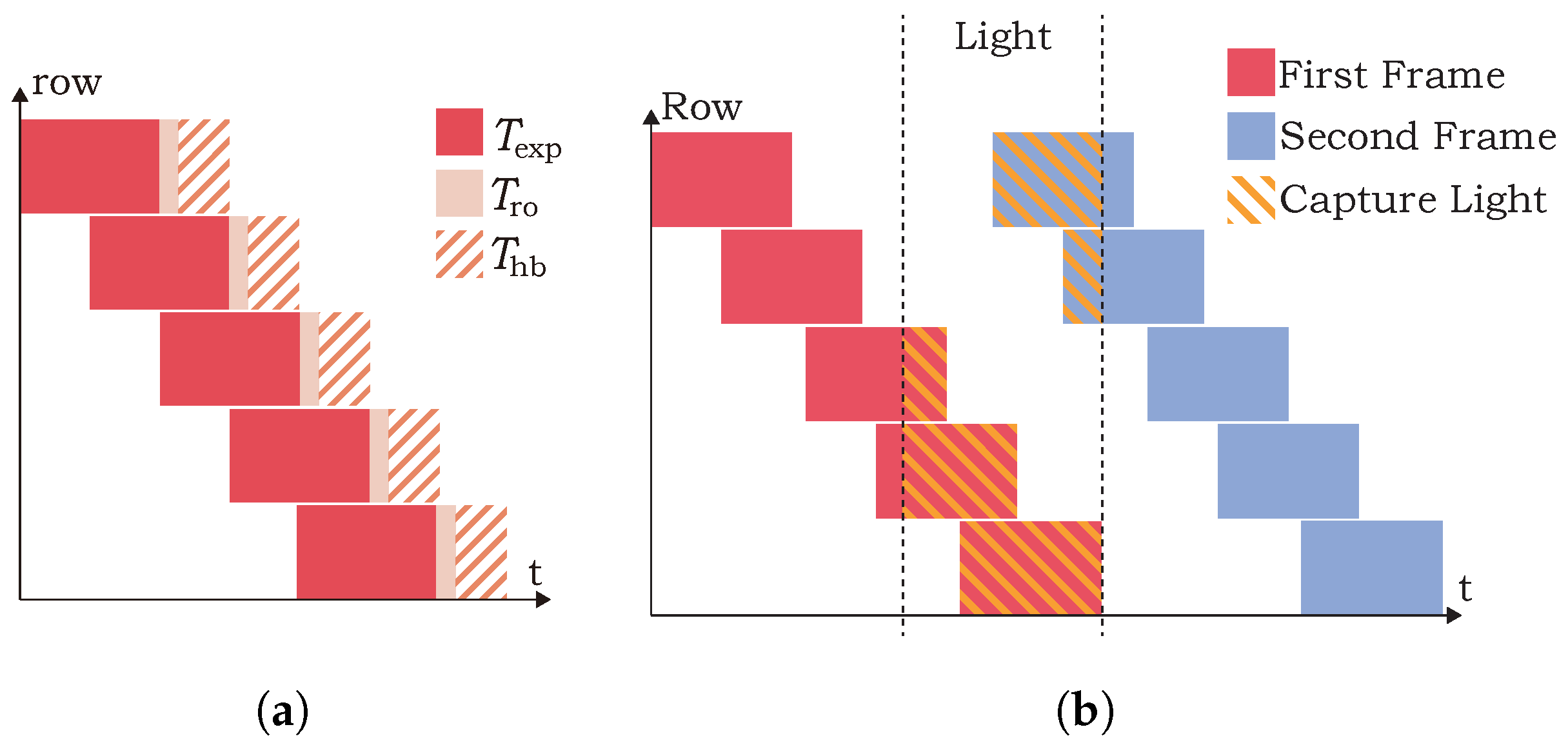
3.2. Duration Control
This paragraph analyzes the various parameters of CMOS, with
Figure 6 displaying the key parameters of exposure.
is the row readout duration, representing the time consumed to read all pixels in one row, and hence it is related to
X, i.e.,
where
is the readout clock frequency.
is the row period, representing the time difference in readout between the previous and the next row, i.e.,
is the vertical blanking duration, representing the time difference between the last
in the previous frame and the first
in the next frame.
is the frame period, representing the time difference in readout between the previous and the next frame, i.e.,
,
,
X,
Y,
, and
are independent variables that can be set through CMOS registers.
NoGap-RS controls
by precisely setting the various parameters of CMOS. An original quantitative relationship between
and parameters can be obtained:
convert to a relationship between
and the independent variables:
By using different parameter sets,
can be controlled.
To quantify the sampling situations of different
, an overlap coefficient
is defined as follows:
where the denominator is the duration of the consecutive-row overlap. The following discusses the sampling situations of different
:
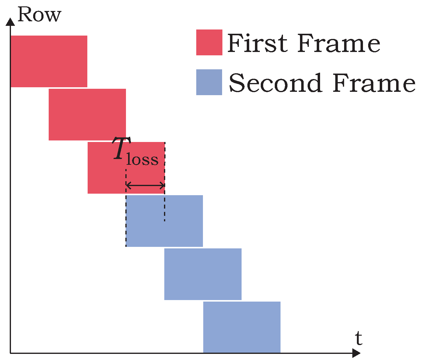
When , . It indicates the presence of signal loss.
When , . It satisfies the minimum requirement of the gapless sampling, where the exposure of the first row in the next frame starts precisely when the exposure of the last row in the previous frame ends.
When , . It indicates the presence of the time overlap during the consecutive-frame exposure.
When
,
, and
. At this point, the first
in the next frame starts precisely when the last
in the previous frame ends, giving the appearance that two frames merge into one frame, thus achieving transparent transmission as shown in
Figure 7. But
is the ideal situation,
has a minimum limitation in hardware, so
can only approach 1.
In practice, making can achieve approximately transparent transmission.
3.3. Theoretical Performance Analysis
This paragraph analyzes the theoretical sampling frequency
of NoGap-RS. In RS-OCC, each exposure represents one sample, and hence
converts to a relationship with the independent variables
This paragraph analyzes the maximum modulation frequency
f of simulating modulation in NoGap-RS.
f is not directly related to
because the sampling of RS-OCC partially overlaps in time, whereas traditional sampling should be independent. Therefore,
f is directly related to
:
This paragraph analyzes the maximum symbol rate of digital modulation in NoGap-RS. Some samples contain the signals of multiple symbols and are considered invalid. In contrast, samples that contain the signal of a single symbol are regarded as valid. As shown in
Figure 8, each symbol should be validly sampled at least twice to distinguish between the valid and the invalid samples. A relationship between the times of the valid sampling
n and
is as follows:
So the symbol rate
B is
This paragraph qualitatively analyzes the impact of the different parameters on performance:
According to Equations (
11) and (
13),
is negatively correlated with the communication rate. However,
should not be too small because the OCC sampling is essentially the process of cumulative exposure. If
is too small, the dynamic range of the signal is limited, thus reducing the ability of the receiver to distinguish between different light levels, which may lead to an increase in Symbol Error Rate (SER).
According to Equation (
13), the sampling count
n is negatively correlated with
B, but if
n is too small, it complicates the receiver’s task of distinguishing sample validity.
According to Equation (
13),
is negatively correlated with
B, but if
is too low, the ratio of
Y to
becomes too low, which means a higher frequency of nearly the transparent transmissions, potentially leading to an increase in SER.
4. TickRS: A Time-Slot-Division Sampling Method Based on NoGap-RS
The goal of this section is to design a time slot division mechanism called TickRS to better utilize high-density pixel arrays in order to improve sampling speed. The approach involves precisely dividing each exposure into multiple Ticks based on the
control method proposed in
Section 3, and utilizing the partial correlation of the exposure values of neighboring rows to calculate the exposure value within each Tick.
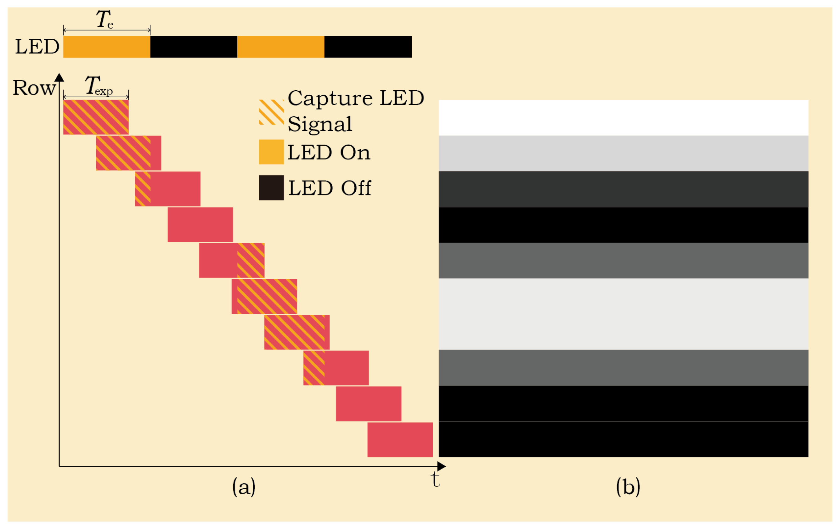
4.1. Tick Division
We divide each exposure into
N Ticks, the duration
of each Tick being the same as the time
to read out a row of pixels. Obviously, the exposure duration
should be an integer multiple of
, and the total number of Ticks per frame is
, recorded as
S, where
Y is the number of rows of CMOS.
Figure 9 is a simple example of TickRS for two consecutive frames, with
,
, and
.
4.2. Tick Solution
Theoretically, it can be considered that the light signal in the same Tick has the same effect on all pixels being exposed, and the exposure of each pixel can be considered the sum of the light signals of all Ticks in the exposure period. Therefore, we have the following formula for the exposure value
c of each pixel:
where
y is the number of the row where the pixel is located, and
is the light signal of the
yth Tick. Taking
Figure 9 as an example, for all rows of pixels, we have the following equation:
where
is the statistical value of the exposure values of all pixels in the first row, which depends on the algorithm used to select the column pixels. And
is the light signal of the first Tick of the frame. At the receiver,
is a known value, and
is a value to be calculated. Obviously, this equation has multiple solutions.
In order to make the equation have a unique solution, we define a constant light value
that is larger than the upper limit value
for the pixel exposure value. Then we let the LED continue to emit light for a certain time in each frame cycle so that the exposure value of at least one row of pixels in each frame of the CMOS reaches
. When the exposure value of a row of pixels is
, the light signal of all Ticks in the exposure period of the pixel is the known value
so that Equation (
15) has a unique solution. It should be noted that
is the maximum value of valid information, and
is a value set to distinguish valid information from constant light signals. Neither of them is the full trap capacity of the pixel.
4.3. Constant Light Signal Duration
OCC can be considered asynchronous communication, and the sender does not know the frame timing of the receiver during operation. Therefore, the constant light signal of the LED emitter may occur partly in the previous frame of the receiver and partly in the next frame. At this time, the constant light signal must last for Ticks to guarantee that the exposure value of a row of pixels in each frame is .
However, the constant light signal is not valid data. The length of the constant light signal is determined by
N, so a too large
N will cause a loss in the Tick efficiency
p, which violates the original intention of TickRS. The specific quantitative relationship between
N and
p is as follows:
where
E is the number of valid Ticks in a frame.
4.4. Sampling Rates and Performance Analysis
The number of samples per second is the number of frames per second multiplied by the number of valid Ticks per frame, so the sampling rate
has the following equation:
where
is
minus the number of clock cycles consumed per frame, so
has the following equation:
substituting in
Next, we explore the impact of
,
Y, and
N on
and sampling delay
.
is defined as the average time from each valid Tick in the frame to the end of the output of the last row of pixels in the frame. The
is fixed at 120 MHz.
Figure 10a shows
and
when
= 1970. The horizontal axis is the number of rows
Y in the exposure window. It can be seen from
Figure 10a that the smaller the number of Ticks
N, the larger the
. This is because when
N increases, the Tick efficiency
p decreases.
As Y increases, also increases, but increases, so comprehensive consideration should be given. And when the signal region is very small, in order to minimize the blank period between frames, Y should also be as small as possible. In addition, if a serious deviation occurs within a Tick, it may cause an error in the entire frame, and an excessively large Y means that there are more valid Ticks in a frame, and SER will increase.
Figure 10b shows
and
when
Y = 480, with
as the horizontal axis. It can be seen that as
increases,
decreases and
increases, so
should not be too large. However, CMOS sampling is not instantaneous and requires a cumulative exposure process. Therefore, a too small
causes the optical signal in a period to be excessively dispersed into multiple consecutive Ticks, which does not help reduce SER, and even requires more calculations to recover information during demodulation, so
should not be too small. In addition, an excessively large
will also cause
to be too long, causing overexposure.
5. TickRS-CSK
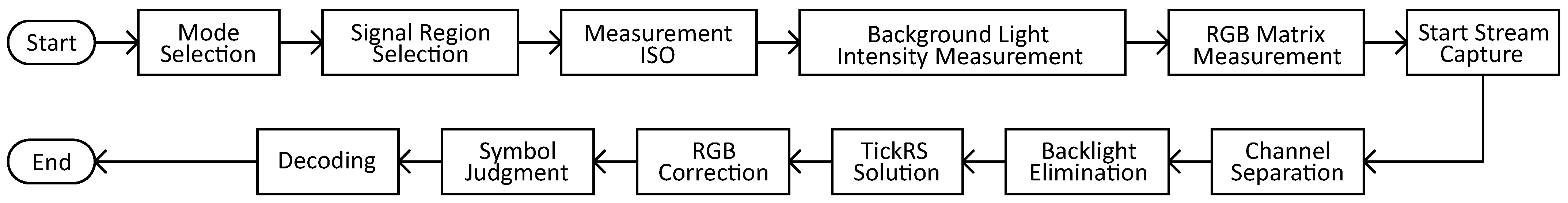
This section constructs TickRS-CSK, a complete receiving process for RS-OCC, based on the CSK modulation and TickRS. CSK employs different colors as different symbols, and uses a constellation map based on color space to decide symbols. In OCC-based CSK, different LEDs can emit the visible light of three wavelengths, and CMOS receives and distinguishes them through a Color Filter Array (CFA), which separates pixels into three channels (usually red, green, and blue) based on the optical wavelength. CSK improves the spectral utilization of visible light in the OCC system.
Figure 11 is the specific process of TickRS-CSK.
5.1. TickRS Under CFA
TickRS is a pixel-level method that focuses on the exposure timing of each row of pixels, which means that TickRS-CSK needs to directly receive signals from pixels from the three channels simultaneously. However, not every row contains pixels from all three channels. Take the following Bayer array as an example:. Each row contains pixels from two channels, resulting in unsynchronized exposure between different channels. Therefore, TickRS requires certain modifications to be applicable to CSK.
Obviously, the red and blue pixels are arranged in alternate rows, which means that the interval between the red and blue pixels starting to be exposed is two Ticks. According to the principle of TickRS, only the total light signal of two Ticks can be solved at this time, so the red and blue pixels can only be solved with two Ticks as a unit for TickRS;
N is an even number. However, green pixels are present in every row, and the number is twice that of the red or blue pixels. The paper uses only the green pixels in odd rows, and also solves them with two Ticks as a unit, aligned with the unit of blue pixels as shown in
Figure 12.
It should be noted that in order to ensure that all color channels can be sampled continuously, the frame interval is reduced by one Tick in quasi-overlap mode. Therefore, the total effective Ticks
E in the frame and the frame rate
of TickRS under CSK modulation both change, so
also changes:
After each color group is solved, the units of different colors are arranged in the timeline as shown in
Figure 12.
5.2. Background Light Measurement
First, capture a frame with a preset exposure time. If the signal region pixels are full, change the preset parameters. Then, in order to fully utilize the ADC range to prevent overflow or loss of accuracy, determine the appropriate analog gain. Algorithm 1 calculates the analog gain, and also outputs the background light intensity
, which is a three-dimensional RGB vector for the subsequent RGB correction.
| Algorithm 1 Calculate and |
| Input: , and ; |
| Output: and ;
|
- 1:
Turn on all LEDs; - 2:
; - 3:
repeat - 4:
; - 5:
; - 6:
Capture signal region with and ; - 7:
Output raw ; - 8:
until - 9:
Turn off all LEDs; - 10:
Capture signal region with and ; - 11:
Output raw ; - 12:
- 13:
return and .
|
5.3. RGB Correction
What needs to be emphasized is the color difference problem, that is, the color received by the receiver is different from the color sent by the sender. There are three main reasons:
White balance: CMOS usually responds more strongly to a certain frequency of light than other colors, usually green, and the raw data has not been white balanced, so it appears to be severely green.
Inter-channel interference: The frequency response curves of the Bayer array for different colors of light overlap, that is, the same color of light may affect multiple pixels of different colors at the same time [
25].
Heterogeneity of CMOS and LED: The spectrum curve of LED and the frequency response curve of the CMOS Bayer array are not completely matched.
Therefore, it is necessary to correct the RGB value before CSK demodulation. The correction method proposed by [
25] is applied to TickRS-CSK. The calculation method of the correction matrix
is different from the original method. Algorithm 2 is its algorithm flow, the matrix
comes from Algorithm 1, and
is the inverse of the PWM resolution of the sender, that is, the upper limit value
of the signal.
After TickRS is solved,
is subtracted from the result and then corrected by Equation (
21).
is the light signal of the red pixel unit of the receiver, which is the value before calibration;
is the corrected value of the unit, which is the estimated value of the original light signal at the sender:
| Algorithm 2 Calculate |
| Input: , N, and ; |
| Output: ;
|
- 1:
Turn on red LED; - 2:
Capture signal region with ; - 3:
Output raw ; - 4:
; - 5:
Turn off red LED; - 6:
- 7:
Turn on green LED brightest; - 8:
Capture signal region with ; - 9:
Output raw ; - 10:
; - 11:
Turn off green LED; - 12:
- 13:
Turn on blue LED brightest; - 14:
Capture signal region with ; - 15:
Output raw ; - 16:
; - 17:
- 18:
; - 19:
return .
|
5.4. Symbol Synchronization
According to Nyquist theorem, the symbol rate
. In other words, the symbols of the emitter are likely to be distributed between two units of the receiver. In order to correctly recover the symbols, the symbol period should be at least twice
. In addition, the receiver needs to recover the clock of the sender to determine which units represent a complete symbol [
23]. Therefore, in this experiment, the sender inserts four groups of ‘01’ before the constant light signal of each color channel in the first frame at the beginning of communication, with turning off the LED as ‘0’ and
as ‘1’.
7. Conclusions and Discussion
The paper presented and elaborated on NoGap-RS, which effectively addresses the technical challenge of signal loss in the RS-OCC system by implementing the programmable control of sampling parameters, thereby significantly enhancing the upper limit of the RS-OCC’s communication rate. Theoretically, NoGap-RS can be combined with most modulation schemes to improve the communication rate of the RS-OCC system. In addition, the SoC, operating system, and CMOS interface protocol of the experimental platform are similar to most mobile devices, suggesting that NoGap-RS is compatible with most mobile phones to some extent, which expands the applicability of NoGap-RS.
In addition, the paper further explored the potential of NoGap-RS and developed TickRS, a high rate method based on time slot division. The TickRS-CSK achieved a BER of 4.36% at a rate of 20.09 Kbps and a distance of 3.6 m, while at a shorter distance of 0.6 m, the data rate of 41.14Kbps exceeded most conventional RS-OCC systems, demonstrating the potential of NoGap-RS and TickRS in high-rate OCC field. Future investigations will focus on extensive experimental validation across multiple CMOS platforms, outdoor light scenarios, and artificial light scenarios with power line interference.


