Abstract
We propose a micro-electromechanical system (MEMS)-integrated Fabry–Pérot (F–P) microcavity designed for a tunable single-photon source based on a single semiconductor quantum dot (QD). Through theoretical simulations, our design achieved a Purcell factor of 23, a photon extraction efficiency exceeding 88%, and an optical cavity mode tuning range of more than 30 nm. Experimentally, we fabricated initial device prototypes using a micro-transfer printing process and demonstrated a tuning range exceeding 15 nm. The device exhibits high mechanical stability, full reversibility, and minimal hysteresis, ensuring reliable operation over multiple tuning cycles. Our findings highlight the potential of MEMS-integrated F–P microcavities for scalable, tunable single-photon sources. Furthermore, reaching a strong coupling regime could enable efficient single-photon routing, opening new possibilities for integrated quantum photonic circuits.
1. Introduction
Single-photon sources with high indistinguishability, purity, and extraction efficiency are crucial components for quantum communication [1], quantum computing [2], and quantum metrology [3]. Indistinguishability ensures that photons are identical across all degrees of freedom (e.g., polarization, wavelength, and temporal profile), a prerequisite for interference-based protocols, such as boson sampling and quantum teleportation. Meanwhile, high purity—quantified by the suppression of multi-photon emission (antibunching)—is critical for maintaining security in quantum key distribution (QKD). Additionally, efficient photon extraction is essential for realizing scalable quantum networks and fault-tolerant architectures.
Among solid-state quantum emitters, semiconductor quantum dots (QDs) have emerged as a leading platform due to their near-unity quantum efficiency, sub-natural emission linewidths, and compatibility with on-chip photonic integration [4,5,6,7,8]. A pivotal strategy for enhancing QD performance involves coupling their emission to high-quality (high-Q) photonic microcavities [9,10,11]. Such integration leverages the Purcell effect [12], which accelerates spontaneous emission rates, thereby improving photon indistinguishability by reducing dephasing effects, while simultaneously boosting extraction efficiency via directional emission into cavity modes. However, optimizing these benefits necessitates stringent alignment conditions: precise spatial overlap between the QD dipole and the cavity mode maximum, and spectral resonance between the QD emission wavelength and the cavity mode. While deterministic spatial alignment has been achieved through advanced optical positioning techniques [13,14,15,16,17], spectral matching remains a critical challenge due to inherent inhomogeneities in QD growth and fabrication-induced cavity resonance shifts.
Conventional spectral tuning methods face significant limitations. Temperature control [18] and the optical Stark effect [19] offer restricted tuning ranges (~0.5 nm for temperature tuning in micropillar cavities [20,21,22]) and often degrade photon coherence or stability. Open-cavity [23,24] enables broadband spectral tuning via mechanical adjustment of distributed Bragg reflector (DBR) mirror gap using nano-positioners, but their reliance on bulky external actuators introduces vibrational sensitivity and scalability barriers. Similarly, electrically tunable QD-microcavity systems employing p-i-n junctions achieve ~18 nm tuning [25,26] yet suffer from free carrier absorption losses in high-Q cavities and reduced quantum efficiency due to field-induced electron-hole wavefunction separation. Piezoelectric tuning [27,28], though mechanically robust, has demonstrated limited ranges (~1.3 nm in our prior work [29]); however, this is insufficient for full spectral alignment in practical devices.
Micro-electromechanical systems (MEMS) technology presents a compelling alternative, combining rapid actuation speeds (>MHz), sub-nanometer precision, and monolithic integration compatibility. Unlike thermally or electrically driven methods, MEMS-based tuning minimizes susceptibility to environmental perturbations and electrostatic fluctuations, ensuring long-term stability. Mechanically adjustable cavities, for instance, enable wavelength tuning exceeding 30 nm in vertical-cavity surface-emitting lasers (VCSELs) [30,31,32,33], highlighting MEMS’ potential for quantum photonics. Critically, MEMS architecture circumvents the trade-offs inherent to doping-dependent or field-sensitive approaches, preserving cavity Q-factors and emitter quantum efficiency.
In this work, we demonstrate a MEMS-integrated QD-microcavity platform achieving a record spectral tuning range of 15 nm—an order-of-magnitude improvement over existing piezoelectric methods—while maintaining high mechanical stability and integration density. By synergizing MEMS actuation with micro-transfer printing for deterministic QD positioning, we realize dynamic, post-fabrication resonance control without compromising cavity performance. This platform addresses the longstanding spectral alignment challenge in quantum photonics, offering a scalable pathway toward wavelength-multiplexed quantum networks and fault-tolerant quantum processors.
2. Device Design and Simulation
2.1. MEMS-Integrated Tunable Fabry–Pérot Cavity Design
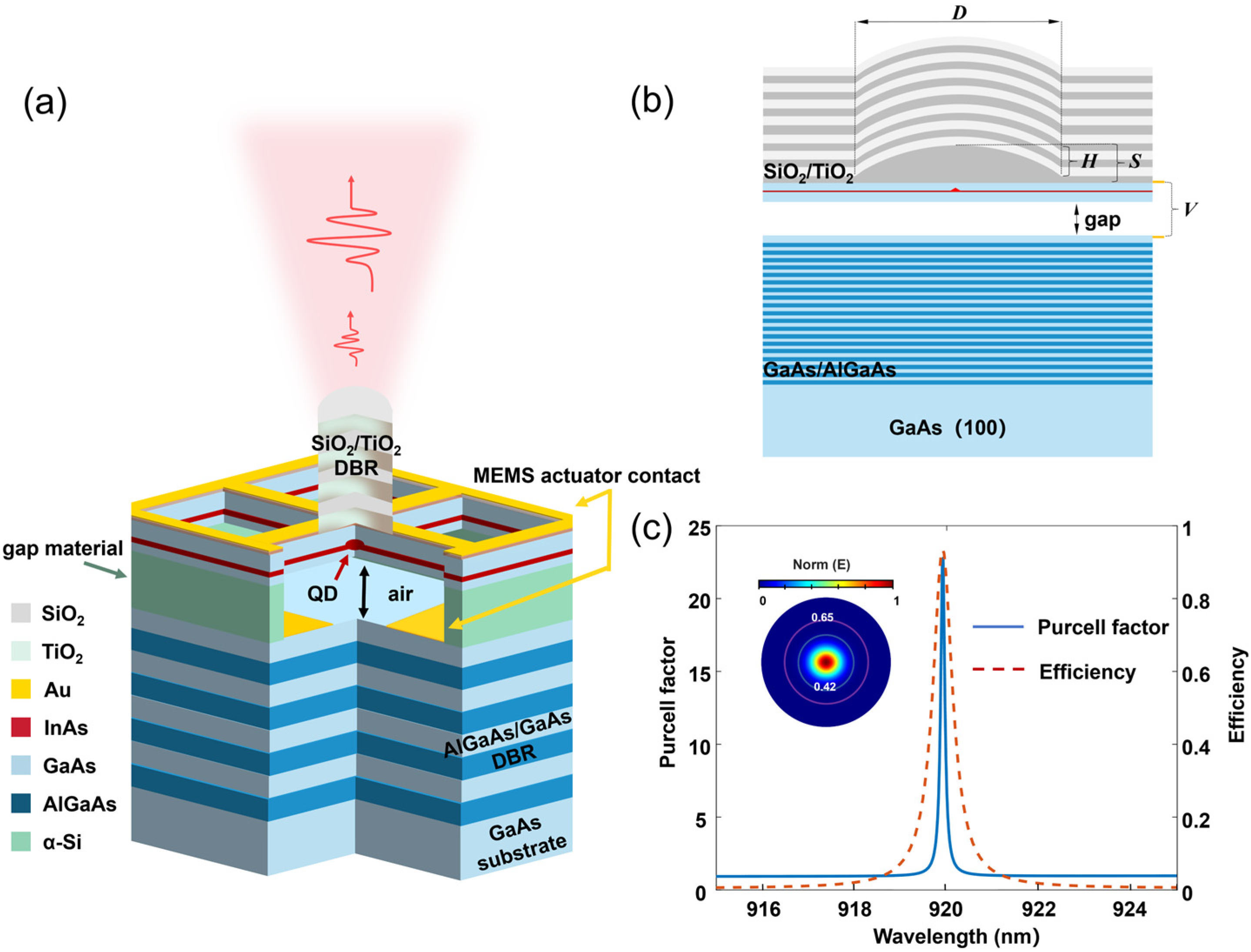
To achieve a high-brightness single-photon source with enhanced emission rates, we designed a tunable Fabry–Pérot (F–P) microcavity that integrates a precisely positioned QD within the cavity, as shown in Figure 1a. This design leverages the Purcell effect to enhance spontaneous emission rates while maintaining compatibility with scalable photonic integration schemes. To realize scalable integration, we developed a dynamically tunable F–P microcavity incorporating a deterministically positioned QD, as illustrated in Figure 1a.

Figure 1.
(a) Schematic diagram of a single-photon source integrated with a tunable Fabry–Pérot microcavity; (b) Cross-sectional view of the optical microcavity, showing the parabolic lens defect with dimensions as follows: diameter D = 4 μm, height H = 300 nm, and spacing S = 480 nm; (c) Simulated performance metrics: Purcell factor = 23, photon extraction efficiency > 92%, and Gaussian transverse optical mode profile.
The cavity architecture comprises top and bottom DBRs encapsulating a GaAs spacer layer embedded with InAs QDs. The top DBR consists of 7 pairs of SiO2/TiO2 (refractive indices nSiO2 = 1.48, nTiO2 = 2.24), while the bottom DBR features 46 pairs of lattice-matched GaAs/Al0.95Ga0.05As (nGaAs = 3.55, nAlGaAs = 3.05), each layer designed at λ/4n thickness for λ = 920 nm. A parabolic SiO2 lens defect (diameter D = 4 μm, height H = 300 nm, spacing S = 480 nm) is integrated into the top DBR to enable transverse optical confinement, reducing mode volume and enhancing extraction efficiency via Gaussian-like far-field profiles [29,34]. The air gap between the GaAs spacer and the top DBR serves as the tuning region, dynamically modulated by a MEMS electrostatic actuator.
The MEMS actuator employs a hybrid upper capacitor plate (300-nm Au/undoped GaAs bilayer) and a fixed lower electrode (150-nm Si-doped GaAs, 2 × 1018 cm−3), separated by a 1-μm air gap. Applying a voltage induces electrostatic forces that displace the upper plate, tuning the cavity length L and resonance wavelength λc. Modeled as a parallel-plate capacitor, the displacement of the MEMS plate () as a function of applied voltage () follows the relation [35]
where is the dielectric constant of air, is the electrode area, is the spring constant, and is the initial air gap thickness. By modulating the applied voltage, we achieve precise control over the cavity resonance wavelength, ensuring alignment with the QD emission spectrum. While simplified as a parallel-plate capacitor for analytical modeling, practical MEMS dynamics necessitate three-dimensional finite element analysis (FEA) to account for material anisotropy, mechanical stress, and electrostatic fringing fields [36,37].
2.2. Optical and Mechanical Co-Design
To realize high-performance single-photon emission with exceptional indistinguishability and efficiency, we adopt a co-design strategy that simultaneously optimizes optical Purcell enhancement and MEMS-based mechanical tunability. The Purcell factor , quantifying the spontaneous emission rate enhancement, is governed by spatial, spectral, and polarization overlap between the QD dipole and the cavity mode [38,39,40]:
where is the total quality factor, is the mode volume, is the cavity resonance wavelength, is the refractive index of the medium in which the dipole is located, is the emitter dephasing rate, and are the linewidth and the central frequency of the cavity mode, and is the frequency of the dipole. and are the electric field strength at the QD and the strongest electric field strength in the cavity mode, and is the strength of the electric dipole. The three multiplicative terms represent spectral detuning, spatial field localization, and dipole-cavity polarization alignment, respectively. Maximizing suppresses non-radiative decay channels, directly enhancing photon indistinguishability.
Photon extraction efficiency is concurrently optimized through cavity outcoupling engineering [21,41]:
where is the probability of photon emission into the cavity mode, and is the extraction efficiency of a photon out of the top DBRs. is the rate at which the photon leaks from the top, while is the rate of photon loss, related to scattering, absorption and leakage from the bottom DBRs. is the rate of spontaneous radiation coupled to other modes.
Three-dimensional finite-difference time-domain (FDTD) modeling optimized the cavity geometry, as shown in Figure 1b, achieving a simulated Q-factor of 104, a Purcell factor Fp = 23, and photon extraction efficiency η > 88% (Figure 1c). The Gaussian transverse mode profile ensured efficient fiber coupling. Detailed geometry parameter sweeps (e.g., lens defect dimensions) are provided in our previous work [29]. A 150-nm Si-doped GaAs layer (doping concentration: 2 × 1018 cm−3) in the bottom DBR provided electrical functionality without compromising optical performance.
For MEMS actuation stability, FEA was applied to a forked Au/GaAs cantilever beam structure (Figure 2a), designed to minimize stress concentrations and align with micro-transfer printing constraints [42]. Material parameters included GaAs (Young’s modulus E = 85.9 GPa, Poisson’s ratio ν = 0.31, density= 5316 kg/m3, a relative permittivity= 12) and Au (E = 70 GPa, ν = 0.44, density = 19,300 kg/m3). Fixed boundary conditions constrained the cantilever beam edges, while the cantilever beam assumes linear elasticity and satisfies electrostatic charge conservation. The entire Au layer serves as the high-potential terminal, forming a capacitor with the fixed lower electrode (zero-potential) and a 1-μm air gap. Electromechanical coupling integrates the electrostatic system with solid mechanics to simulate voltage-induced displacement.
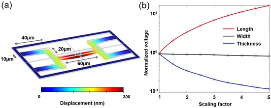
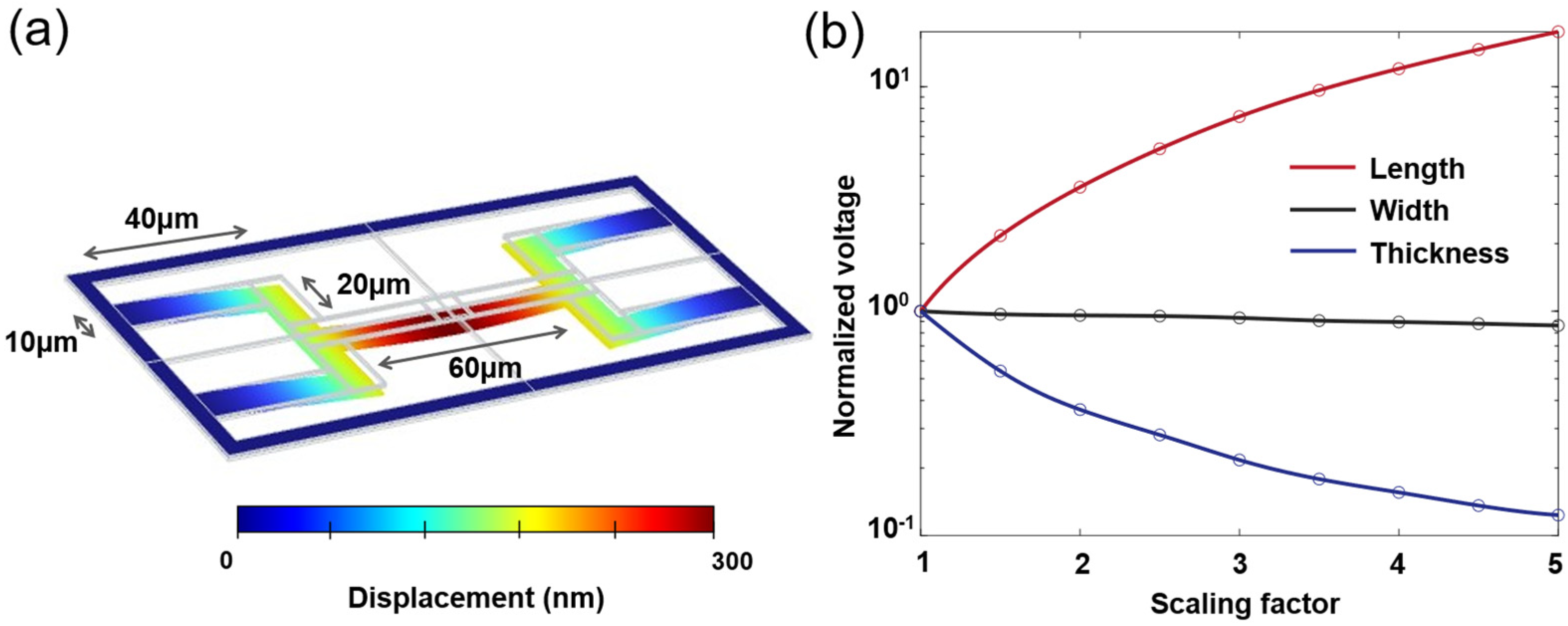
Figure 2.
(a) Deformation of a forked cantilever beam structure under a reverse-bias voltage of 5 V: the length and width are respectively 70 μm and 10 μm; (b) parametric scan results for cantilever beam dimensions: the three parameters are the length, width, and thickness of the cantilever beam. The scaling factor on the x-axis refers to the dimensional reduction ratio, while the voltage on the y-axis corresponds to the normalized applied voltage to achieve a 100 nm displacement for beams with the respective scaled dimensions.
Parametric sweeps revealed beam length L and thickness t as dominant factors in stiffness, with negligible width dependence. A 50% reduction in beam length (scaling factor = 2) decreased the required actuation voltage by 64%, underscoring the importance of geometric miniaturization for low-power operation (Figure 2b). Voltage-controlled displacement of the GaAs thin film enabled precise tuning of the cavity resonance, with simulations showing a 300 nm displacement under voltages below 6 V, corresponding to a 30 nm resonance shift (Figure 3). This level of tunability meets the experimental requirements for aligning pre-characterized QD emission wavelengths with the cavity mode.
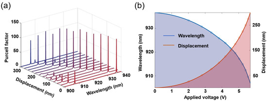
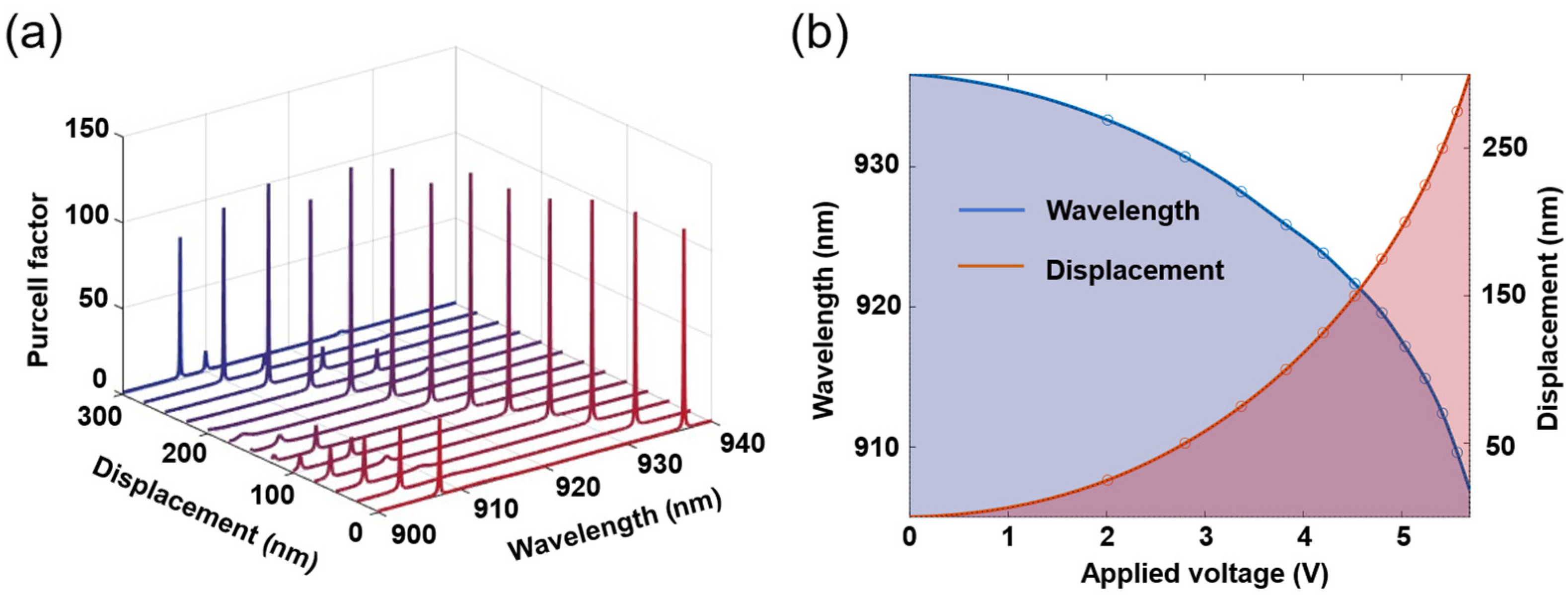
Figure 3.
(a) Simulation diagram of cavity mode corresponding to the displacement of the thin film: the curve color represents the cavity mode shift with displasment; (b) scanning results of the voltage sweep: based on the cantilever beam structure described above, the displacement of the structure at different voltages and the corresponding cavity modes are observed. A displacement of approximately 100 nm results in a 10 nm wavelength tuning, with a total tuning of 30 nm achieved at voltages below 6 V.
3. Device Fabrication and Characterization
3.1. Fabrication Process
The MEMS-integrated tunable F–P microcavity was fabricated through a multi-step nanofabrication protocol combining epitaxial growth, lithographic patterning, and micro-transfer printing. The process commenced with the molecular beam epitaxy (MBE) growth of a heterostructure on a GaAs substrate, sequentially comprising a 46-pair GaAs/Al0.8Ga0.2As bottom DBR with each layer designed at λ/4n thickness (λ = 920 nm), a 1-μm Al0.8Ga0.2As sacrificial layer, a GaAs spacer layer (twice the wavelength at 920 nm) embedded with InAs QDs, and a 7-pair SiO2/TiO2 top DBR deposited via electron beam evaporation. A parabolic SiO2 lens defect (4 μm diameter, 300 nm height, 480 nm spacing) was patterned onto the top DBR using electron-beam lithography and inductively coupled plasma (ICP) to enable transverse optical confinement. A 300-nm Au layer was subsequently deposited via electron-beam evaporation to form the upper MEMS electrode, followed by the fabrication of a GaAs cantilever beam through ICP etching. Parallel fabrication of the lower MEMS module involved sequential deposition of an Au lower electrode and a 1.5-μm amorphous silicon (a-Si) sacrificial layer via inductively coupled plasma chemical vapor deposition (ICP–CVD).
Critical alignment between the upper and lower modules was achieved through micro-transfer printing. The Al0.8Ga0.2As sacrificial layer was selectively etched using a HCl:H2O (1:1) solution to release the upper structure, which remained anchored to the substrate via photoresist tethers. A polydimethylsiloxane (PDMS) stamp, aligned via real-time image recognition [42], bonded to the released structure and transferred it onto the lower MEMS module with sub-50 nm positional accuracy. The a-Si sacrificial layer was then removed using SF6 plasma etching to define the air gap, followed by O2 plasma descumming to eliminate residual photoresist.
Scanning electron microscopy (SEM) confirmed the successful integration of the MEMS actuator, revealing a fully suspended forked cantilever beam with a 1-μm air gap (Figure 4a). The initial cantilever position under zero bias exhibited sub-nanometer curvature, establishing a stable mechanical baseline for electrostatic actuation experiments. This fabrication methodology ensures precise spatial alignment and mechanical stability while enabling seamless integration with heterogeneous material systems.
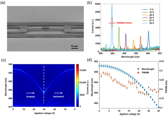
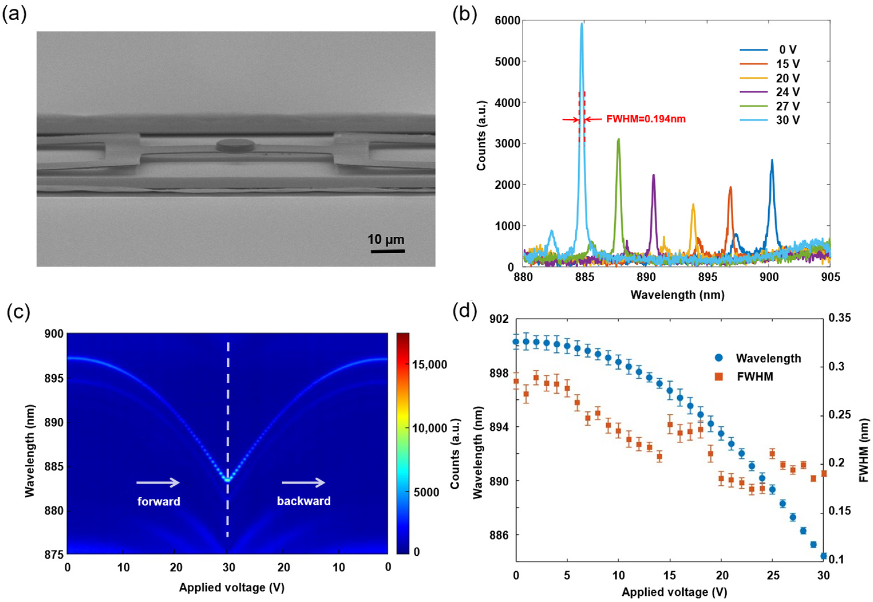
Figure 4.
(a) Scanning electron microscopy (SEM) image of the fabricated device, showing the forked cantilever beam and microcavity structure, with scale bar of 10 μm; (b) frequency distribution of microcavity modes under a continuous 785 nm laser at different voltages, with FWHM fitted using a Lorentzian function; (c) voltage cycling test: wavelength tuning spectra recorded during voltage application (0–30 V) and release (back to 0 V); (d) cavity resonance wavelength and FWHM as a function of applied voltage: the voltage increases from 0 to 30 V, yielding a tuning range of 15.80 ± 0.15 nm. The blue circles (left y-axis) correspond to the resonance wavelength with error bars representing the standard deviation of the fitting residuals, scaled by a factor of one hundred for clarity. The red squares (right y-axis) correspond to the FWHM values with the error bars denoting the same fitting uncertainty.
3.2. Microavity Tunability
The spectral tunability of the MEMS-integrated microcavity was characterized by applying DC voltages (0–30 V) to the electrostatic actuator (Figure 4b). Increasing the voltage induced a monotonic reduction in the air gap due to cantilever displacement, thereby blue-shifting the cavity resonance wavelength. The device achieved a continuous tuning range exceeding 15 nm under applied voltages below 30 V, demonstrating the key advantage of low-voltage operation while avoiding pull-in instability—a critical limitation in electrostatic MEMS, where abrupt contact occurs beyond a threshold voltage [35,36,37]. The pull-in voltage, governed by the initial air gap and spring constant, was precisely engineered through geometric optimization of the cantilever (length L = 80 μm, thickness t = 520 nm) to balance tunability and reliability. Reducing air gap lowers the pull-in threshold but risks surface adhesion and Casimir forces at sub-500 nm gaps, necessitating a design compromise to ensure stable actuation cycles.
Spectral characterization revealed a Lorentzian cavity mode centered at 884.440 ± 0.002 nm with a linewidth of 0.194 ± 0.003 nm (FWHM), corresponding to a quality factor Q > 4500 (Figure 4b). The high Q-factor, measured using a spectrometer with 0.01 nm resolution, underscores the preserved optical coherence despite mechanical actuation—a critical requirement for quantum interference protocols. Voltage cycling tests further validated the mechanical robustness: over 100 actuation cycles, the resonance wavelength exhibited reversible shifts < 0.1 nm (from 900.28 nm to 900.20 nm) with no observable hysteresis or structural fatigue (Figure 4c). Systematic analysis of voltage-dependent tuning (Figure 4d) quantified the center wavelength shift (Δλ) and linewidth stability. The standard deviation of Lorentzian fit residuals remained below 0.005 nm for the center wavelength λc and 0.007 nm for FWHM, confirming sub-picometer actuation precision. This combination of wide tunability and mechanical robustness establishes the MEMS-integrated microcavity as a promising platform for wavelength-multiplexed quantum networks and scalable quantum photonic circuits.
4. Summary and Discussion
In this work, we demonstrate a MEMS-integrated tunable F–P microcavity designed for quantum photonic applications. By utilizing a suspended cantilever beam architecture, we achieved electrostatic control over the cavity resonance wavelength with a continuous tuning range exceeding 15 nm under low driving voltages (≤30 V) while maintaining a high quality factor (Q > 4500). The device exhibited exceptional mechanical stability, showing negligible hysteresis (<0.1 nm) and fully reversible cavity mode shifts over repeated voltage cycles. A key innovation of this platform lies in its integrated and scalable design, which enables precise, low-power, and high-speed resonance tuning—advantages that starkly contrast with conventional thermal or piezoelectric methods. This makes the system highly compatible with on-chip quantum light sources and photonic circuits, addressing a critical need for scalable quantum technologies.
However, challenges remain in the practical implementation of MEMS-integrated F–P cavities. Fabrication complexity, involving over ten lithographic steps, introduced defects that reduced device yield by 20%. Post-release cantilever deformation due to residual stress relaxation and adhesive forces (Figure 4a) increased the air gap, altering the cavity length L and inducing higher-order transverse modes. This nonlinearity compromises tuning efficiency, as described by Δλ/λ = ΔL/L, and necessitates higher actuation voltages (Equation (1)). Furthermore, phase coupling effects in multi-layer cavities (air gap, semiconductor layers, and DBRs) introduce additional nonlinear dependencies between air gap displacement and effective phase accumulation [43]. To mitigate these limitations, future efforts will prioritize in situ stress monitoring during fabrication, material optimization (e.g., low-stress SiNx films), hybrid electrostatic–thermal actuation schemes, and supercritical dry and machine learning-enhanced process control to improve yield and tuning linearity.
The next critical milestone involves integrating this tunable microcavity with deterministically positioned QDs to realize a frequency-agile single-photon source. Our molecular beam epitaxy-grown InAs QDs exhibit emission wavelengths spanning 910–940 nm, which can be spectrally filtered and spatially mapped via confocal fluorescence imaging. By pre-engineering cavity parameters (e.g., air gap, lens defect geometry) to align the cavity mode near target QD wavelengths, the MEMS tuning capability enables post-fabrication spectral matching—ensuring spatial, spectral, and polarization overlap (Equation (2)) to maximize Purcell enhancement and photon extraction efficiency. Advancing this system into the strong coupling regime could further enable coherent light-matter interactions, unlocking functionalities such as single-photon routing and non-classical state manipulation. The platform’s compatibility with standard semiconductor fabrication techniques positions it as a cornerstone for scalable quantum photonic circuits, paving the way for integrated single-photon sources, wavelength-multiplexed networks, and fault-tolerant quantum processors—essential components for future quantum communication and computing architectures.
Author Contributions
Conceptualization, Z.Z. and Y.Y.; methodology, Z.Z., J.Y. and Y.Y.; validation, Z.Z., J.Y. and Y.Y.; investigation, Z.Z., J.Y., X.P. and Y.Y.; writing—original draft preparation, Z.Z.; writing—review and editing, Z.Z. and Y.Y.; project administration, Y.Y.; funding acquisition, Y.Y. All authors have read and agreed to the published version of the manuscript.
Funding
This research was funded by the National Natural Science Foundation of China (12474397, 62422516); Innovation Program for Quantum Science and Technology (2021ZD0301400).
Institutional Review Board Statement
Not applicable.
Informed Consent Statement
Not applicable.
Data Availability Statement
The data presented in this study are available from the corresponding authors upon reasonable request.
Conflicts of Interest
The authors declare no conflicts of interest.
References
- Yin, J.; Cao, Y.; Li, Y.H.; Liao, S.K.; Zhang, L.; Ren, J.G.; Cai, W.Q.; Liu, W.Y.; Li, B.; Dai, H.; et al. Satellite-Based Entanglement Distribution over 1200 Kilometers. Science 2017, 356, 1140–1144. [Google Scholar] [CrossRef] [PubMed]
- Wang, H.; Qin, J.; Ding, X.; Chen, M.C.; Chen, S.; You, X.; He, Y.M.; Jiang, X.; You, L.; Wang, Z.; et al. Boson Sampling with 20 Input Photons and a 60-Mode Interferometer in a 1014-Dimensional Hilbert Space. Phys. Rev. Lett. 2019, 123, 250503. [Google Scholar] [CrossRef] [PubMed]
- Peniakov, G.; Su, Z.-E.; Beck, A.; Cogan, D.; Amar, O.; Gershoni, D. Towards Supersensitive Optical Phase Measurement Using a Deterministic Source of Entangled Multiphoton States. Phys. Rev. B 2020, 101, 245406. [Google Scholar] [CrossRef]
- Bradac, C.; Gao, W.; Forneris, J.; Trusheim, M.E.; Aharonovich, I. Quantum Nanophotonics with Group IV Defects in Diamond. Nat. Commun. 2020, 11, 5625. [Google Scholar] [CrossRef]
- Santori, C.; Fattal, D.; Vuckovic, J.; Solomon, G.S.; Yamamoto, Y. Indistinguishable Photons from a Single-Photon Device. Nature 2002, 419, 594–597. [Google Scholar] [CrossRef]
- Meraner, M.; Mazloom, A.; Krutyanskiy, V.; Krcmarsky, V.; Schupp, J.; Fioretto, D.A.; Sekatski, P.; Northup, T.E.; Sangouard, N.; Lanyon, B.P. Indistinguishable Photons from a Trapped-Ion Quantum Network Node. Phys. Rev. A 2020, 102, 052614. [Google Scholar] [CrossRef]
- McKeever, J.; Boca, A.; Boozer, A.D.; Miller, R.; Buck, J.R.; Kuzmich, A.; Kimble, H.J. Deterministic Generation of Single Photons from One Atom Trapped in a Cavity. Science 2004, 303, 1992–1994. [Google Scholar] [CrossRef]
- He, Y.-M.; Clark, G.; Schaibley, J.R.; He, Y.; Chen, M.-C.; Wei, Y.-J.; Ding, X.; Zhang, Q.; Yao, W.; Xu, X.; et al. Single Quantum Emitters in Monolayer Semiconductors. Nat. Nanotechnol. 2015, 10, 497–502. [Google Scholar] [CrossRef]
- Chen, Y.; Zopf, M.; Keil, R.; Ding, F.; Schmidt, O.G. Highly-Efficient Extraction of Entangled Photons from Quantum Dots Using a Broadband Optical Antenna. Nat. Commun. 2018, 9, 2994. [Google Scholar] [CrossRef]
- Liu, S.F.; Wei, Y.M.; Li, X.S.; Yu, Y.; Liu, J.; Yu, S.Y.; Wang, X.H. Dual-Resonance Enhanced Quantum Light-Matter Interactions in Deterministically Coupled Quantum-Dot-Micropillars. Light Appl. 2021, 10, 158. [Google Scholar] [CrossRef]
- Liu, J.; Su, R.B.; Wei, Y.M.; Yao, B.M.; da Silva, S.F.C.; Yu, Y.; Iles-Smith, J.; Srinivasan, K.; Rastelli, A.; Li, J.T.; et al. A Solid-State Source of Strongly Entangled Photon Pairs with High Brightness and Indistinguishability. Nat. Nanotechnol. 2019, 14, 586–593. [Google Scholar] [CrossRef] [PubMed]
- Purcell, E.M. Spontaneous Emission Probabilities at Radio Frequencies BT—Confined Electrons and Photons: New Physics and Applications; Burstein, E., Weisbuch, C., Eds.; Springer: Boston, MA, USA, 1995; p. 839. ISBN 978-1-4615-1963-8. [Google Scholar]
- Kaganskiy, A.; Gschrey, M.; Schlehahn, A.; Schmidt, R.; Schulze, J.H.; Heindel, T.; Strittmatter, A.; Rodt, S.; Reitzenstein, S. Advanced in-Situ Electron-Beam Lithography for Deterministic Nanophotonic Device Processing. Rev. Sci. Instrum. 2015, 86, 073903. [Google Scholar] [CrossRef] [PubMed]
- Dousse, A.; Lanco, L.; Suffczyński, J.; Semenova, E.; Miard, A.; Lemaître, A.; Sagnes, I.; Roblin, C.; Bloch, J.; Senellart, P. Controlled Light-Matter Coupling for a Single Quantum Dot Embedded in a Pillar Microcavity Using Far-Field Optical Lithography. Phys. Rev. Lett. 2008, 101, 267404. [Google Scholar] [CrossRef] [PubMed]
- Gschrey, M.; Thoma, A.; Schnauber, P.; Seifried, M.; Schmidt, R.; Wohlfeil, B.; Krüger, L.; Schulze, J.-H.; Heindel, T.; Burger, S.; et al. Highly Indistinguishable Photons from Deterministic Quantum-Dot Microlenses Utilizing Three-Dimensional in Situ Electron-Beam Lithography. Nat. Commun. 2015, 6, 7662. [Google Scholar] [CrossRef]
- Thon, S.M.; Rakher, M.T.; Kim, H.; Gudat, J.; Irvine, W.T.M.; Petroff, P.M.; Bouwmeester, D. Strong Coupling through Optical Positioning of a Quantum Dot in a Photonic Crystal Cavity. Appl. Phys. Lett. 2009, 94, 111115. [Google Scholar] [CrossRef]
- Sapienza, L.; Davanco, M.; Badolato, A.; Srinivasan, K. Nanoscale Optical Positioning of Single Quantum Dots for Bright and Pure Single-Photon Emission. Nat. Commun. 2015, 6, 7833. [Google Scholar] [CrossRef]
- Unsleber, S.; He, Y.-M.; Gerhardt, S.; Maier, S.; Lu, C.-Y.; Pan, J.-W.; Gregersen, N.; Kamp, M.; Schneider, C.; Hoefling, S. Highly Indistinguishable On-Demand Resonance Fluorescence Photons from a Deterministic Quantum Dot Micropillar Device with 74% Extraction Efficiency. Opt. Express 2016, 24, 8539–8546. [Google Scholar] [CrossRef]
- Finley, J.J.; Sabathil, M.; Vogl, P.; Abstreiter, G.; Oulton, R.; Tartakovskii, A.I.; Mowbray, D.J.; Skolnick, M.S.; Liew, S.L.; Cullis, A.G.; et al. Quantum-Confined Stark Shifts of Charged Exciton Complexes in Quantum Dots. Phys. Rev. B 2004, 70. [Google Scholar] [CrossRef]
- Wang, H.; He, Y.-M.; Chung, T.-H.; Hu, H.; Yu, Y.; Chen, S.; Ding, X.; Chen, M.-C.; Qin, J.; Yang, X.; et al. Towards Optimal Single-Photon Sources from Polarized Microcavities. Nat. Photonics 2019, 13, 770–775. [Google Scholar] [CrossRef]
- Nowak, A.K.; Portalupi, S.L.; Giesz, V.; Gazzano, O.; Dal Savio, C.; Braun, P.-F.; Karrai, K.; Arnold, C.; Lanco, L.; Sagnes, I.; et al. Deterministic and Electrically Tunable Bright Single-Photon Source. Nat. Commun. 2014, 5, 3240. [Google Scholar] [CrossRef]
- Ding, X.; He, Y.; Duan, Z.C.; Gregersen, N.; Chen, M.C.; Unsleber, S.; Maier, S.; Schneider, C.; Kamp, M.; Höfling, S.; et al. On-Demand Single Photons with High Extraction Efficiency and Near-Unity Indistinguishability from a Resonantly Driven Quantum Dot in a Micropillar. Phys. Rev. Lett. 2016, 116, 020401. [Google Scholar] [CrossRef] [PubMed]
- He, Y.-M.; He, Y.; Wei, Y.-J.; Wu, D.; Atatuere, M.; Schneider, C.; Hoefling, S.; Kamp, M.; Lu, C.-Y.; Pan, J.-W. On-Demand Semiconductor Single-Photon Source with Near-Unity Indistinguishability. Nat. Nanotechnol. 2013, 8, 213–217. [Google Scholar] [CrossRef] [PubMed]
- Tomm, N.; Javadi, A.; Antoniadis, N.O.; Najer, D.; Löbl, M.C.; Korsch, A.R.; Schott, R.; Valentin, S.R.; Wieck, A.D.; Ludwig, A.; et al. A Bright and Fast Source of Coherent Single Photons. Nat. Nanotechnol. 2021, 16, 399. [Google Scholar] [CrossRef] [PubMed]
- Somaschi, N.; Giesz, V.; De Santis, L.; Loredo, J.C.; Almeida, M.P.; Hornecker, G.; Portalupi, S.L.; Grange, T.; Antón, C.; Demory, J.; et al. Near-Optimal Single-Photon Sources in the Solid State. Nat. Photonics 2016, 10, 340–345. [Google Scholar] [CrossRef]
- Bennett, A.J.; Pooley, M.A.; Stevenson, R.M.; Ward, M.B.; Patel, R.B.; De Giroday, A.B.; Sköld, N.; Farrer, I.; Nicoll, C.A.; Ritchie, D.A.; et al. Electric-Field-Induced Coherent Coupling of the Exciton States in a Single Quantum Dot. Nat. Phys. 2010, 6, 947–950. [Google Scholar] [CrossRef]
- Lettner, T.; Gyger, S.; Zeuner, K.D.; Schweickert, L.; Steinhauer, S.; Hedlund, C.R.; Stroj, S.; Rastelli, A.; Hammar, M.; Trotta, R.; et al. Strain-Controlled Quantum Dot Fine Structure for Entangled Photon Generation at 1550 Nm. NANO Lett. 2022, 22, 4285. [Google Scholar] [CrossRef]
- Chen, Y.; Zhang, J.; Zopf, M.; Jung, K.; Zhang, Y.; Keil, R.; Ding, F.; Schmidt, O.G. Wavelength-Tunable Entangled Photons from Silicon-Integrated III–V Quantum Dots. Nat. Commun. 2016, 7, 10387. [Google Scholar] [CrossRef]
- Yang, J.; Chen, Y.; Rao, Z.; Zheng, Z.; Song, C.; Chen, Y.; Xiong, K.; Chen, P.; Zhang, C.; Wu, W.; et al. Tunable Quantum Dots in Monolithic Fabry-Perot Microcavities for High-Performance Single-Photon Sources. Light Appl. 2024, 13, 33. [Google Scholar] [CrossRef]
- Cole, G.D.; Behymer, E.; Bond, T.C.; Goddard, L.L. Short-Wavelength MEMS-Tunable VCSELs. Opt. Express 2008, 16, 16093–16103. [Google Scholar] [CrossRef]
- Wang, M.; PENG, H.; Hao, C.; Zhou, X.; Zheng, W.; Liu, A. Detector-Integrated Vertical-Cavity Surface-Emitting Laser with a Movable High-Contrast Grating Mirror. Photonics Res. 2024, 12, 1437–1448. [Google Scholar] [CrossRef]
- Li, K.; Chase, C.; Rao, Y.; Chang-Hasnain, C.J. Widely Tunable 1060-Nm High-Contrast Grating VCSEL. In Proceedings of the 2016 Compound Semiconductor Week (CSW) [Includes 28th International Conference on Indium Phosphide & Related Materials (IPRM) & 43rd International Symposium on Compound Semiconductors (ISCS), Toyama, Japan, 26–30 June 2016; pp. 1–2. [Google Scholar] [CrossRef]
- Chase, C.; Zhou, Y.; Chang-Hasnain, C.J. Size Effect of High Contrast Gratings in VCSELs. Opt. Express 2009, 17, 24002. [Google Scholar] [CrossRef] [PubMed]
- Ding, F.; Stoeferle, T.; Mai, L.; Knoll, A.; Mahrt, R.F. Vertical Microcavities with High Q and Strong Lateral Mode Confinement. Phys. Rev. B 2013, 87, 161116(R). [Google Scholar] [CrossRef]
- Ferrara, J.E. High Contrast Metastructures on Silicon for Optoelectronic Devices, University of California. 2015. Available online: https://www2.eecs.berkeley.edu/Pubs/TechRpts/2017/EECS-2017-12.pdf (accessed on 7 April 2023).
- Cole, G.D.; Björlin, E.S.; Chen, Q.; Chan, C.Y.; Wu, S.M.; Wang, C.S.; MacDonald, N.C.; Bowers, J.E. MEMS-Tunable Vertical-Cavity SOAs. IEEE J. Quantum Electron. 2005, 41, 390–407. [Google Scholar] [CrossRef]
- Mateus, C.F.R.; Huang, M.C.Y.; Chang-Hasnain, C.J. Micromechanical Tunable Optical Filters: General Design Rules for Wavelengths from near-IR up to 10μm. Sensors Actuators A Phys. 2005, 119, 57–62. [Google Scholar] [CrossRef]
- Gayral, B.; Gérard, J.M. Strong Purcell Effect for InAs Quantum Boxes in High-Q Wet-Etched Microdisks. Phys. E 2000, 7, 641–645. [Google Scholar] [CrossRef]
- Vyshnevyy, A.A. Gain-Dependent Purcell Enhancement, Breakdown of Einstein’s Relations, and Superradiance in Nanolasers. Phys. Rev. B 2022, 105, 085116. [Google Scholar] [CrossRef]
- Krasnok, A.; Alu, A. Active Nanophotonics. Proc. IEEE 2020, 108, 628–654. [Google Scholar] [CrossRef]
- Barbour, R.J.; Dalgarno, P.A.; Curran, A.; Nowak, K.M.; Baker, H.J.; Hall, D.R.; Stoltz, N.G.; Petroff, P.M.; Warburton, R.J. A Tunable Microcavity. J. Appl. Phys. 2011, 110, 053107. [Google Scholar] [CrossRef]
- Goyvaerts, J.; Kumari, S.; Uvin, S.; Zhang, J.; Baets, R.; Gocalinska, A.; Pelucchi, E.; Corbett, B.; Roelkens, G. Transfer-Print Integration of GaAs p-i-n Photodiodes onto Silicon Nitride Waveguides for Near-Infrared Applications. Opt. Express 2020, 28, 21275–21285. [Google Scholar] [CrossRef]
- Larson, M.C. Microelectromechanical Wavelength-Tunable Vertical-Cavity Light-Emitters and Lasers, Stanford University. 1996. Available online: https://www.proquest.com/pqdtglobal (accessed on 20 July 2024).
Disclaimer/Publisher’s Note: The statements, opinions and data contained in all publications are solely those of the individual author(s) and contributor(s) and not of MDPI and/or the editor(s). MDPI and/or the editor(s) disclaim responsibility for any injury to people or property resulting from any ideas, methods, instructions or products referred to in the content. |
© 2025 by the authors. Licensee MDPI, Basel, Switzerland. This article is an open access article distributed under the terms and conditions of the Creative Commons Attribution (CC BY) license (https://creativecommons.org/licenses/by/4.0/).