Article

Topological Rainbow Trapping with Expanded Bandwidth in Valley Photonic Crystals

1
Physics Department, Faculty of Science, Assiut University, Assiut 71516, Egypt
2
College of Physics and Optoelectronic Engineering, Shenzhen University, Shenzhen 518060, China
3
Department of Physics, College of Science, Imam Mohammad Ibn Saud Islamic University, Riyadh 11432, Saudi Arabia
4
Department of Optics and Photonics, National Central University, Taoyuan City 320, Taiwan
*
Authors to whom correspondence should be addressed.
Photonics 2025, 12(5), 487; https://doi.org/10.3390/photonics12050487
Submission received: 1 April 2025 / Revised: 4 May 2025 / Accepted: 13 May 2025 / Published: 14 May 2025
(This article belongs to the Special Issue Photonics Metamaterials: Processing and Applications)

Abstract

:
We introduce a novel approach to achieve broadband rainbow trapping in a 2D photonic crystal (PC) platform. By exploiting the concept of valley PCs, we engineer a structure that supports robust topological edge states. A carefully designed rotational angle gradient along the edge state path induces frequency-dependent light localization, forming a topological rainbow with a significantly expanded bandwidth. This phenomenon of topological rainbow trapping is attributed to the interplay between valley-dependent topological edge states and the engineered rotational angle gradient. To further enhance light localization and broaden the trapping spectrum, we incorporate a graded radius profile in the bottom row of dielectric columns. Through a combination of rotational angle modulation and radius grading, we successfully realize broadband rainbow trapping with enhanced light localization. Our findings reveal a broad trapping bandwidth spanning from 0.8314 c / a to 0.9205 c / a , showcasing the potential of this approach for applications in optical frequency filtering, sensing, and information processing.

1. Introduction

The manipulation and control of light at the nanoscale level has been a cornerstone of scientific and technological advancement [1,2,3]. Photonic crystals (PCs), periodic structures that modulate light propagation, have emerged as a promising platform for achieving unprecedented control over light flow [4,5,6,7,8,9,10,11]. In recent years, exploring topological phenomena in photonic systems has opened up new avenues for designing innovative optical devices with unprecedented functionalities [12,13,14,15]. Among these, valley topological PCs have garnered significant attention due to their ability to support topologically protected edge states, characterized by their robustness to defects and disorder [16,17,18,19,20]. These properties hold immense potential for applications in various fields, including optical communication, sensing, and information processing.
In recent years, there has been a growing interest in developing methods for controlling the frequency-dependent behavior of light within PC structures. This has led to exploring strategies for achieving broadband light manipulation, essential for various applications, including optical communication, sensing, and imaging. One particularly intriguing phenomenon is the creation of a “topological rainbow”, where light of different frequencies is localized at distinct spatial positions within a PC structure [21,22,23,24,25,26]. This phenomenon is attributed to the interplay between the valley-dependent topology of the system and the engineered structural gradients.
The core of the design is a two-dimensional (2D) PC platform. Leveraging a square lattice structure with judiciously designed circular dielectric columns, we induce topological phase transitions by manipulating rotational symmetry with varying radii arranged in a specific pattern by carefully adjusting the rotational angle gradient of these columns along the edge state path. This gradient induces a frequency-dependent modulation of light propagation, resulting in the localization of different frequencies at specific points within the structure, forming a topological rainbow. This phenomenon arises from the interplay between the valley-dependent topological edge states (TESs) and the engineered rotational angle gradient.
Moreover, introducing a graded radius profile to the dielectric columns further enhances light localization and broadens the trapping spectrum. This approach offers several advantages over existing methods. Firstly, the utilization of valley topological PC ensures the robustness of the TESs, making the system resilient to imperfections and disorder. Secondly, the combination of rotational angle modulation and radius grading allows for a significant enhancement in light localization and a broadening of the trapping spectrum. Consequently, we achieve a broadband rainbow trapping with a bandwidth spanning from 0.8314 c / a to 0.9205 c / a , surpassing the limitations of previous approaches. This study presents a groundbreaking advance in the field of PCs by demonstrating broadband rainbow trapping through the integration of valley topological photonics and carefully engineered structural parameters. These findings pave the way for developing novel photonic devices with enhanced functionalities and open up new possibilities for applications in optical communication, sensing, and information processing.

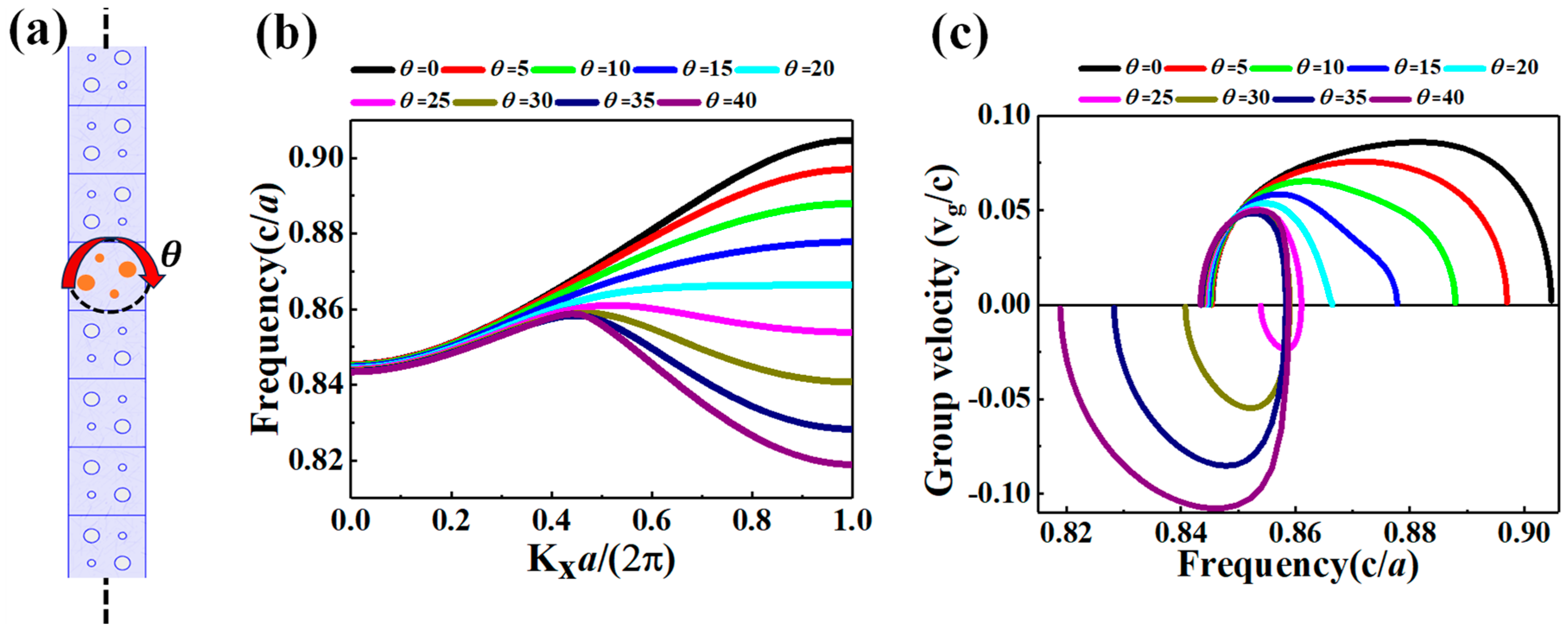
2. Valley Topological PC and Photonic Band Structures

A 2D PC based on a square lattice was designed, consisting of four circular dielectric columns embedded in an air background. The rods have radii r 1 = 0.05 a and r 2 = 0.1 a , where a = 1000   n m is the lattice constant. Each rod is positioned at a distance l = 0.20 a from the unit cell (UC) center that supports symmetry manipulation. The dielectric rods have a refractive index of n = 3.46 , which is representative of silicon in the infrared regime. Figure 1a shows the three UC configurations used throughout the study, each representing a distinct symmetry or perturbation. To analyze the photonic band structure, the finite element method (FEM) was employed via COMSOL Multiphysics (version 6.2), applying periodic boundary conditions and computing along the high-symmetry path Γ–X–M–Γ of the first Brillouin zone (BZ). The focus was on transverse magnetic (TM) modes with non-zero components E z , H x , and H y . For TM polarization, the governing Maxwell equation for electromagnetic wave propagation in the PC is given by [5]:
× 1 ε r × E z r = ω 2 c 2 E z r ,
where ε ( r ) is the position-dependent permittivity, ω is the angular frequency, and c is the speed of light in the vacuum. The corresponding magnetic field components H x , and H y are derived from E z using Faraday’s law: H = i / ( μ 0 ω ) × E , assuming vacuum permeability μ 0 . Due to the periodicity of the dielectric structure, the out-of-plane electric field component E z ( r ) can be expanded using Bloch’s theorem:
E z r = u n k ( r ) e i k . r ,
where u n k is the periodic part of the Bloch function for the n th band. This periodic function can be further expanded in a Fourier series over reciprocal lattice vectors:
u n k r = G E k n G e i G . r ,
Substituting this into Maxwell’s equations and applying orthogonality of plane waves leads to the eigenvalue problem [27]:
G κ G G k + G 2 E k n G = ω k n 2 c 2 E k n G ,
where κ G is the Fourier component of 1 / ε ( r ) . By solving this eigenvalue problem using FEM with periodic boundary conditions, the eigenfrequency ω k n and Fourier coefficients E k n G of the corresponding eigenmode can be obtained, leading to the photonic band structures, as shown in Figure 1b–d. The formation of topological phases in PCs fundamentally relies on symmetry breaking, which modifies the degeneracies and field distributions of photonic modes [28,29,30,31]. Two primary methods of symmetry breaking are commonly used: (i) shifting the positions of adjacent rods to break inversion symmetry, or (ii) rotating dielectric rods to perturb mirror and rotational symmetries. In this study, we adopt the latter method by introducing a rotational angle θ for the rods, enabling controlled topological transitions within the same lattice geometry.
To understand the topological origin of the valley-protected edge states in the designed PC, we analyze the evolution of the photonic band structure and field characteristics associated with the three rotational configurations of UCs, illustrated in Figure 1a. In the unrotated configuration θ = 0 (Figure 1b), the structure preserves both mirror and inversion symmetry. This high-symmetry state results in multiple clear photonic bandgaps for TM modes and supports degenerate modes at certain high-symmetry points, leading to topologically trivial bands. At intermediate rotation θ = 45 (Figure 1c), symmetry is partially broken, lifting degeneracies and inducing accidental Dirac points, and linear band crossings away from high-symmetry points (highlighted by the red dashed line) [32,33]. These crossings arise due to the hybridization of photonic modes carrying opposite orbital angular momentum, signaling a critical point in a topological phase transition [34,35]. The Berry curvature becomes non-zero near these valleys, and multiple peaks appear, implying potential non-trivial topological indices [34,36]. Upon further rotation to θ = 90 (Figure 1d), symmetry breaking is maximized again but with an inverted topological character. The bandgap reopens with opposite Berry curvature signs compared to θ = 0 , completing the topological phase transition. The effective Hamiltonian governing this valley Hall transition is: [37,38,39] H e f f ( k ) = v D ( τ k x σ x + k y σ y ) + λ ( θ ) σ z , where v D is the Dirac velocity, τ is the valley index for the two inequivalent momentum valleys, and σ x y z are the Pauli matrices representing the pseudospin degrees of freedom. The term λ ( θ ) is an external perturbative parameter determined by the rotational angle θ. It reflects the degree of inversion and mirror symmetry breaking introduced by rod rotation [40,41]. The Berry curvature is defined via the Berry connection Ω n k = k × A n k , with A n k = i u n k k u n k . In inversion symmetry-broken PCs, this curvature becomes sharply localized near valley centers [42]. Integrating over the Brillouin zone (BZ) gives the valley Chern number C = 1 2 π B Z Ω n k d 2 k . The term λ ( θ ) is an external perturbative parameter determined by the rotational angle θ . The continuous variation λ ( θ ) along the interface results in a graded energy landscape for TESs, which translates into frequency-selective localization. The field distribution maps of the designed valley PC at two symmetry-broken configurations θ = 0 , and θ = 90 were constructed to reflect the vortex behavior of the out-of-plane electric field E z , which was directly extracted at the Dirac point frequency 0.6944 c / a (Figure 1e). At θ = 0 , E z exhibits a clockwise vortex, corresponding to a negative Berry curvature concentrated at the upper valleys and a positive Berry curvature at the lower valleys. In contrast, at θ = 90 , the phase vortex is counterclockwise, yielding an opposite Berry curvature distribution with positive curvature at the upper valleys. This reversal of Berry curvature is a direct consequence of the valley pseudospin switching induced by symmetry manipulation [26]. These antisymmetric Berry curvature distributions are centered at the valley points of the Brillouin zone and serve as the real-space indicator of the valley Hall topological phase transition. The sign reversal leads to a valley Chern number difference of Δ C = 1 between θ = 0 and θ = 90 , ensuring the existence of a robust topological edge mode along their interface, consistent with the bulk-boundary correspondence [13,43,44,45]. Figure 1f shows the projected band structure of a supercell composed of UCs with θ = 0 and θ = 90 , forming a domain wall. A topological edge mode clearly appears inside the bandgap (highlighted in green). The electric field distribution at k x = 1 (red dot) shows strong localization at the interface (right panel), with negligible leakage into the bulk [46]. This is a hallmark of valley Hall topological edge states, confirmed by prior studies [47]. These states are immune to backscattering and remain stable even in the presence of structural disorder, making them suitable for broadband slow-light applications and frequency-dependent light localization.
The capacity to precisely control and localize light within PC structures is paramount for advancing optical technologies. By strategically manipulating the rotational angles of the four circular dielectric columns in the valley topological PC design, we introduce a novel method to achieve highly customizable and robust light confinement. This approach gradually modulates the rotational angle for the four rods (orange color) along the edge state path, as shown in Figure 2a, which subtly alters the TESs by modifying their group velocities, implementing a graded interface to achieve broadband light manipulation. To understand this effect, we analyze the evolution of the TES dispersion curves shown in Figure 2b. As the rotational angle increases, the slope of the TES dispersion curve progressively decreases, indicating a reduction in the group velocity. This modulation is crucial for inducing spatial light localization, as lower group velocities correspond to enhanced energy confinement. The group velocity is defined as: v g = d ω / d k , progressively decreases with the angle gradient. This modulation is crucial for inducing spatial light localization, as lower group velocities correspond to enhanced energy confinement. Figure 2b illustrates this behavior, showing the evolution of the dispersion curves for the TESs as the rotational angle increases from θ = 0 to θ = 40 . The band structure transitions from a positive to an opposing group velocity regime, as depicted in Figure 2c. The group velocity ultimately approaches zero for certain frequency components, forming a localized “slow light” region. This localized region is the fundamental mechanism enabling broadband rainbow trapping. The resulting frequency-dependent control over light propagation forms a topological rainbow, wherein distinct light frequencies are located at specific spatial positions within the structure. This phenomenon is a direct consequence of the interplay between the valley-dependent nature of the TESs and the meticulously engineered rotational angle gradient. The physical origin of this effect lies in the symmetry perturbation induced by the rotational angle gradient. By varying the rotational angle, the inversion symmetry between neighboring unit cells is progressively broken. This perturbation modifies the local dispersion properties, causing different frequency components to propagate at distinct velocities. As a result, different frequencies experience varying delays, effectively leading to spatial separation across the graded structure, which is the signature behavior of the rainbow trapping effect. We have demonstrated an effective method for controlling light propagation and localization within a PC structure by harnessing the intricate relationship between rotational angle, group velocity, and frequency. This approach holds significant potential for applications in optical frequency filtering, wavelength division multiplexing, and other photonic devices.
To further enhance light localization and broaden the rainbow trapping bandwidth, a radial gradient was introduced to the dielectric rods along the propagation path. As illustrated in Figure 3a, the bottom-row rod r d (red) gradually chirped in radius from 0.25 a to 0.29 a . The bottom row does not form a full topological interface; the resonant frequency gradient induced by refractive index modulation that supports gradual frequency localization effectively creates a quasi-1D slow-light path that enables strong localization via slow-light effects. This modulation increases the local dielectric density, effectively raising the refractive index along the direction of light propagation. The adjacent bulk region with non-trivial topology still provides a bandgap barrier, allowing light to remain confined along this quasi-guided path, as shown in Figure 3b, which displays the dispersion relations for different values of r d . The progressive downward shift in the dispersion curves with increasing r d confirms the redshift in modal frequency induced by the structural chirp. Moreover, the structure was engineered such that the effective operating point approaches the band edge, leading to a flattening of the dispersion curves. This behavior is clearly illustrated in Figure 3c, where the group velocity v g decreases significantly for increasing rod radii. The resulting slow light regime stems from the constructive interference of multiple scattering events within the spatially graded medium. The prolonged light–matter interaction enabled by this gradient design opens pathways for enhanced optical confinement and spectral control. Our simulations are intentionally performed in 2D, assuming infinite structural thickness. While in practical three-dimensional structures, parameters such as rod depth indeed influence resonant frequencies and rainbow trapping behavior (see, e.g., Refs. [48,49]), the current design specifically isolates the effects arising solely from the rotational angle gradient and graded radius profile. Investigating additional frequency-tuning mechanisms via structural depth variation potentially extends and further optimizes these trapping phenomena.

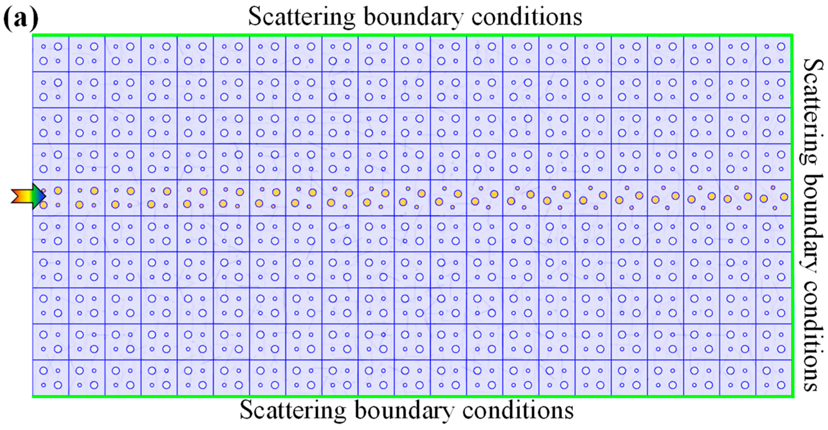
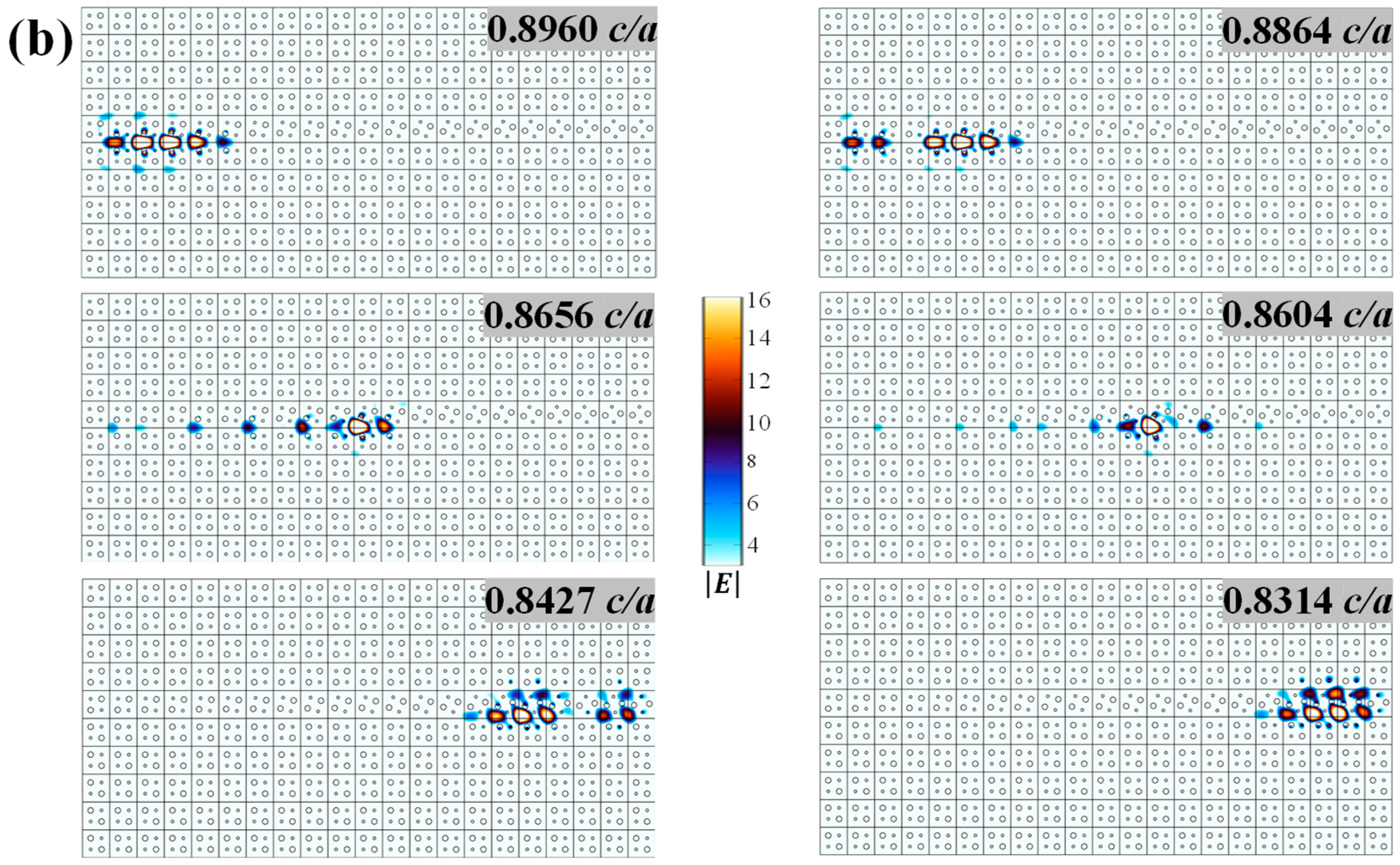
3. Rainbow Trapping Structures

To engineer a rainbow-trapping structure, we designed a valley topological PC with a gradually modulated rotational angle along its edge state path. This was achieved by coupling supercells together, as illustrated in Figure 4a, where the four orange rods define the rotational angle. The graded structure spans 21-unit cells along the x-direction, with the rotational angle of the orange rods increasing from 0 to 40 degrees in 2-degree increments to span the topological bandgap without crossing the Dirac point at 45 , ensuring stable mode confinement and smooth field evolution over 21 units in the propagation direction. The upper unit cells remained constant throughout. To characterize the rainbow trapping phenomenon, FEM simulations were performed using COMSOL Multiphysics. A plane wave broadband source was introduced at the left boundary while scattering boundary conditions were applied to all other sides, as depicted in Figure 4a. This configuration allowed for a comprehensive analysis of the structure’s response to multifrequency light input and the electric field distribution visualization. The origin of rainbow trapping lies in the structure’s dispersive nature. When a spatial gradient in the rotational angle is introduced along the propagation direction (from θ = 0 to θ = 90 across 21 units), each interface segment locally supports a slightly different TES with a distinct dispersion relation. This results in a position-dependent group velocity, as shown in Figure 2b,c. Specifically, the slope of the TES dispersion curve ( v g = d ω / d k ) flattens progressively with increasing θ , indicating a reduction in the group velocity. The slower light is more confined, and near-zero group velocities correspond to frequency components being effectively “trapped” at specific spatial positions. This behavior is physically analogous to an adiabatic modulation of the local photonic potential, where each unit cell along the gradient acts as a locally perturbed resonator with a slightly shifted resonance [50]. This detuning along the interface forms a graded photonic landscape, where light experiences increasing delay as it propagates, leading to the rainbow trapping effect. Importantly, this is achieved without altering the global topology of the structure, thereby maintaining topological protection. Accordingly, by incident broadband plane wave comprises a spectrum of frequencies, and due to the structure’s properties, these frequencies interact differently, leading to distinct propagation delays. This differential delay results in the spatial separation of frequencies, or rainbow trapping, as different frequency components become localized at specific positions within the structure. The engineered rotational angle gradient plays a crucial role in this process. Inducing a frequency-dependent modulation of light propagation enhances light localization and broadens the trapping spectrum. This interplay between valley-dependent TESs and the rotational angle gradient creates a topological rainbow formed, where each frequency component is spatially separated. Our design achieved broadband rainbow trapping with a bandwidth spanning from 0.8314 c / a to 0.8960 c / a , significantly surpassing the capabilities of previous approaches. This is evident in the electric field distribution shown in Figure 4b, where the spatial separation of frequencies across the structure is visible. Although the demonstrated design inherently localizes energy into a relatively narrow spatial region at the topological interface, such strong localization is highly beneficial for specific advanced applications, such as integrated nanolasers [51], optical multiplexers [52], high-Q resonant cavities, and sensors [53,54]. The barrier regions (bulk structures above and below the interface) are critical to maintaining robust topological confinement by preventing scattering or leakage.
A radial gradient was introduced to the dielectric columns in the bottom row of the structure to achieve broadband and spatially localized topological rainbow trapping. This graded configuration consisted of 21 units along the x-axis, with the column radius ( r d ) increasing linearly from 0.25 a to 0.29 a in increments of 0.002 a (Figure 5a). Eigenfrequency simulations were performed using the Wave Optics module in COMSOL Multiphysics to characterize the resonant frequencies and the field within this gradient structure. A 2D cut line was defined along the arc length of the dielectric column gradient (from 0 a to 21 a ) as shown by black and green arrows in Figure 5a, allowing for analysis of the electric field amplitude as a function of both radii ( r d ) and position along the arc length. This analysis revealed a systematic shift in the maximum electric field amplitude position towards larger arc lengths with decreasing frequency, confirming the occurrence of rainbow trapping (Figure 5b). Further validation of the rainbow trapping effect was obtained by simulating the structure’s response to a broadband plane wave source. The resulting electric field distribution (Figure 5c) clearly demonstrated the localization of different frequency components within specific spatial regions, spanning a bandwidth from 0.8657 c / a to 0.9205 c / a . This trapping occurs at frequencies where the group velocity of the slow light mode approaches zero, facilitated by the refractive index gradient induced by the structure. This study demonstrates the realization of broadband and localized topological rainbow trapping, surpassing the limitations of previous approaches. The ability to manipulate and control light frequencies within a compact structure holds promise for various applications. The precise control over frequency localization can enable the development of highly selective optical filters with tailored spectral responses. The sensitivity of the trapped frequencies to environmental changes can be exploited for sensing applications, such as refractive index sensing and biochemical detection. By harnessing the principles of topological photonics and gradient engineering, this work contributes to the advancement of light manipulation and control, with the potential for significant impact across multiple scientific and technological domains [55,56]. While the broadband rainbow trapping presented here is primarily enabled through a spatial gradient in rod radius that tunes local resonances, we note that inter-rod separation can also influence coupling strength and dispersion. However, based on the presented design and trapping mechanism, radius variation is more effective in producing distinct and spatially localized field concentrations.
To further examine the influence of radius variation, we conducted additional simulations where the radius gradient was confined to three distinct subranges, each targeting specific modal regimes. As shown in Figure 6, the monopole region ( 0.05 a 0.08 a ,   s t e p   0.0015 a ) supports simple localized field profiles (Figure 6a), while the dipole range ( 0.12 a 0.17 a ,   s t e p   0.0025 a ) leads to modes with increased spatial symmetry (Figure 6b). The quadrupole regime ( 0.20 a 0.24 a , step 0.002 a ) enables higher-order field confinement (Figure 6c). These results confirm the ability of the proposed design to achieve spatially resolved rainbow trapping across different frequency bands by selectively exciting monopole-, dipole-, and quadrupole-like edge states. Compared to spacing-based modulation, this radius-tuning strategy proves more robust, controllable, and compatible with broadband operation. The modal localization patterns observed here complement the multipolar coexistence region illustrated in Figure 5c, highlighting the flexibility of the design to enable diverse rainbow trapping responses.
The proposed approach combines insights from previous topological rainbow trapping designs while introducing a novel mechanism that leverages the interplay between topological phase transitions and rotational angle gradients. Previous studies have demonstrated broadband topological rainbow trapping using different strategies. For example, in [57], a dual-mode rainbow was obtained via a sandwiched heterostructure structure with a combined bandwidth of ~ 0.038 c / a . Meanwhile, in [24], a cavity-coupled TES was used, achieving a normalized bandwidth of approximately ~ 0.045 c / a (from 0.295 c / a to 0.340 c / a ). However, both methods rely on dual-mode interference or coupled cavities and are either limited in flexibility or involve complex spatial layouts. In contrast, our structure achieves a significantly broader normalized bandwidth of ~ 0.089 c / a (from 0.8314 c / a to 0.9205 c / a ), solely through continuous modulation of rotation angle and rod radius in a single unified interface. This results in a simpler and more compact design, free of external cavities or mode conversion schemes, while preserving topological protection. Additionally, this method allows tunable excitation of different modal families (monopole, dipole, quadrupole), offering a versatile platform for integrated slow-light and light-trapping applications. Thus, the approach not only outperforms previous structures in terms of bandwidth but also demonstrates higher design efficiency and robustness through a single-phase-engineered interface.

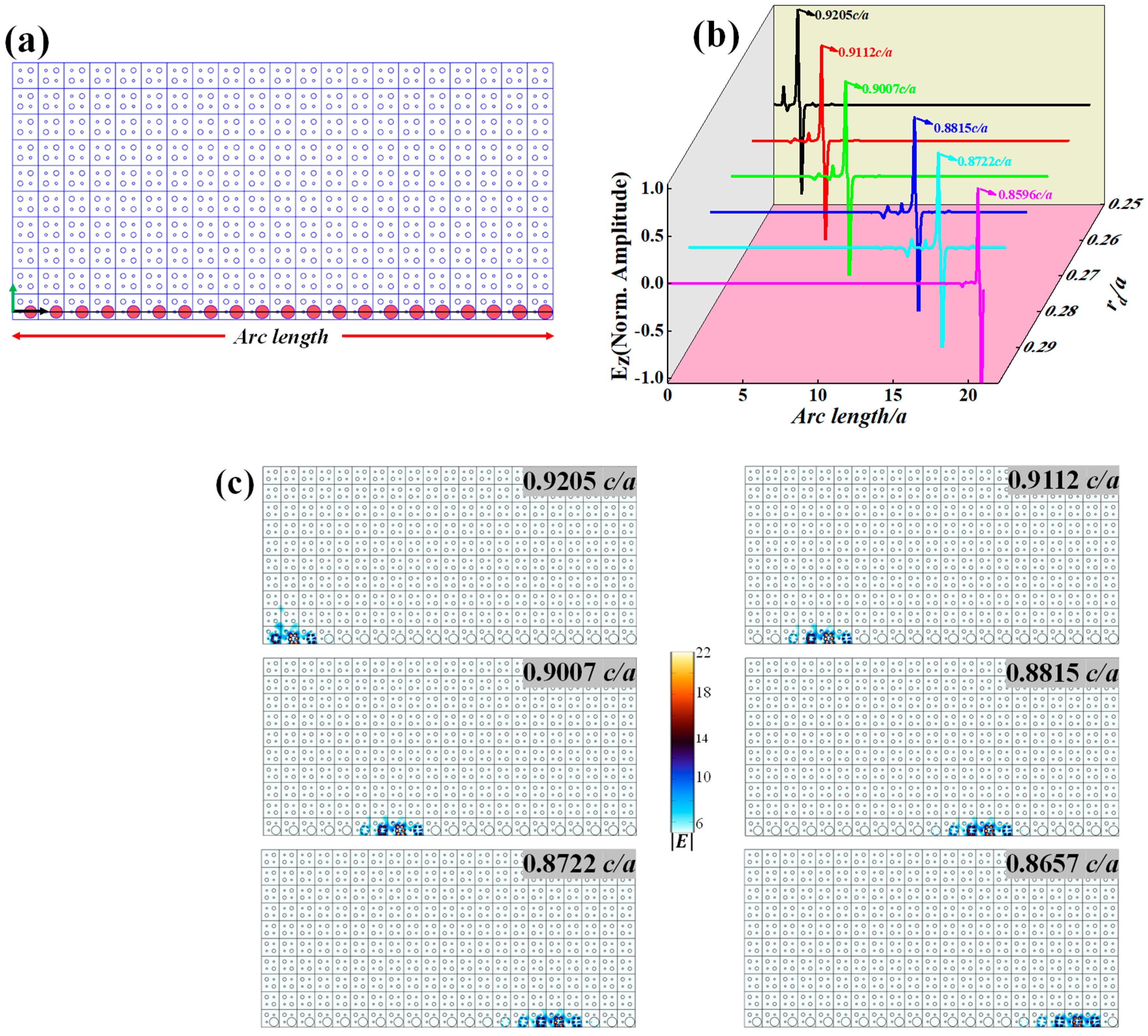
4. Verification of Robustness

We introduced controlled disorder into the system to assess the robustness of our proposed rainbow-trapping design against structural imperfections. Specifically, random displacements and omissions of rods near the edge state path were implemented, as shown in Figure 7a. Disordered rods were shifted by ± 0.05 a in the x or y directions and, in some cases, entirely removed. Remarkably, electric field distributions E at the targeted frequencies ( 0.8960 c / a and 0.8314 c / a ) remained highly localized and largely unaffected by the introduced disorder, demonstrating the intrinsic robustness of the topological rainbow trapping effect (Figure 7b). While minor perturbations in the field distribution were observed near the defect sites at intermediate frequencies (e.g., 0.8687 c / a (II)), the overall rainbow trapping phenomenon persisted. This resilience to disorder can be attributed to the topological protection of the edge states, which renders the system less susceptible to localized perturbations. The robustness of the TESs can be further understood by analyzing the system’s Berry curvature. In the presence of a rotational angle gradient, the Berry curvature becomes asymmetric, resulting in a net accumulation of geometric phases across the structure. This non-trivial curvature leads to non-reciprocal light propagation along the interface, reinforcing the system’s robustness against structural imperfections and disorder. As demonstrated in Figure 7b, even with intentional rod displacement and omissions, the localized field distribution remains robust, confirming the topological protection of the TESs. The observed robustness underscores the potential of this design for practical applications where fabrication imperfections are inevitable. Moreover, the system’s sensitivity to local perturbations suggests a potential avenue for tuning the rainbow trapping characteristics through controlled defect engineering, offering opportunities for dynamic control and modulation of the trapped light.
The proposed PC heterostructure can be fabricated using standard techniques widely employed in photonic device manufacturing [54,58,59,60,61]. Techniques such as electron beam lithography (EBL) and electrochemical etching have proven highly effective for realizing 2D PCs with well-defined rod patterns. In the EBL process, a patterned resist layer is defined on a substrate using electron beam exposure, followed by developing and lift-off procedures to produce the desired rod geometry [62,63]. This approach enables precise control over rod dimensions and orientation, which is essential for realizing the rotational gradient required in the proposed design [64,65,66]. Electrochemical etching offers an efficient method to fabricate large-area PCs using silicon and hydrofluoric acid, providing excellent control over spatial periodicity [67,68]. Meanwhile, direct laser writing (DLW) provides a flexible and accessible alternative for prototyping, allowing on-demand patterning of complex topological structures.
To ensure fabrication accuracy and performance validation, standard characterization techniques can be employed. Scanning electron microscopy can be used to confirm geometric fidelity, while near-field scanning optical microscopy enables spatial mapping of the localized electric fields. Additionally, far-field broadband sources can be used to monitor spectral-spatial separation of light, serving as direct experimental confirmation of the rainbow trapping phenomenon. Robustness to fabrication imperfections can also be evaluated by intentionally introducing rod displacement or defects and observing field confinement behavior.
These fabrication and characterization techniques are well-established in integrated photonics and provide a feasible path to experimentally realize and validate the proposed structure. Thus, the design aligns well with existing fabrication and measurement capabilities and can be integrated into practical photonic devices for sensing, filtering, and light routing.

5. Conclusions

In conclusion, we proposed and demonstrated topological rainbow trapping in two-dimensional valley PCs. The structure possesses a square lattice with circular dielectric columns of varying radii. We achieve robust localization of different frequency components at specific spatial positions by introducing a rotational angle gradient along the edge of a supercell composed of unit cells with distinct topological phases. This phenomenon, termed topological rainbow trapping, is attributed to the interplay between valley-dependent TESs and the engineered rotational angle gradient. Our design exhibits a wide trapping bandwidth and robust light localization, surpassing conventional rainbow trapping methods. This work paves the way for novel photonic devices with enhanced functionality and robustness.

Author Contributions

S.E.S.: Conceptualization, Methodology, Software, Writing—Original draft preparation, Writing—Reviewing and editing. I.A.: Data curation, Software, Visualization, Investigation. N.A.A.: Software, Writing—Reviewing and editing C.-C.C.: Supervision, Funding acquisition, Writing—Reviewing and editing. All authors have read and agreed to the published version of the manuscript.

Funding

This work was granted by the National Science and Technology Council, Taiwan (Grant Nos. NSTC 112-2221-E-008-089 and NSTC 113-2811-E-008-006).

Institutional Review Board Statement

Not applicable.

Informed Consent Statement

Not applicable.

Data Availability Statement

Data will be made available on request.

Conflicts of Interest

The authors declare that they have no known competing financial interests or personal relationships that could have appeared to influence the work reported in this paper.

References

  1. Li, Z.-Y. Optics and photonics at nanoscale: Principles and perspectives. Europhys. Lett. 2015, 110, 14001. [Google Scholar] [CrossRef]
  2. You, J.; Ma, Q.; Zhang, L.; Liu, C.; Zhang, J.; Liu, S.; Cui, T. Electromagnetic metamaterials: From classical to quantum. Electromagn. Sci. 2023, 1, 1–33. [Google Scholar] [CrossRef]
  3. Ai, X.-C.; Pan, S.-C.; Wang, Y.-H.; Tian, S.-C. Optimization Design of Photonic-Crystal Surface-Emitting Lasers: Toward Large Bandwidth and Single-Lane 200G Optical Transmission. Prog. Electromagn. Res. 2024, 180, 89–101. [Google Scholar] [CrossRef]
  4. Firouzjaei, A.S.; Afghahi, S.S.; Valmoozi, A.-A.E. Emerging Trends, Applications, and Fabrication Techniques in Photonic Crystal Technology. In Recent Advances and Trends in Photonic Crystal Technology; IntechOpen: London, UK, 2024. [Google Scholar]
  5. Joannopoulos, J.D.; Johnson, S.G.; Winn, J.N.; Meade, R.D. Photonic Crystals: Molding the Flow of Light, 2nd ed.; Princeton Univ. Press: Princeton, NJ, USA, 2008. [Google Scholar]
  6. Hou, C.-H.; Tseng, S.-Z.; Chan, C.-H.; Chen, T.-J.; Chien, H.-T.; Hsiao, F.-L.; Chiu, H.-K.; Lee, C.-C.; Tsai, Y.-L.; Chen, C.-C. Output power enhancement of light-emitting diodes via two-dimensional hole arrays generated by a monolayer of microspheres. Appl. Phys. Lett. 2009, 95, 133105. [Google Scholar] [CrossRef]
  7. Cheng, Y.C.; Cai, D.P.; Chen, C.C.; Chan, C.H.; Lee, C.C.; Tsai, Y.L. Photonic Crystal Cavity with Double Heterostructure in GaN Bulk. IEEE Photonics J. 2013, 5, 2202606. [Google Scholar] [CrossRef]
  8. Hsiao, F.-L.; Ni, C.-Y.; Tsai, Y.-P.; Chiang, T.-W.; Yang, Y.-T.; Fan, C.-J.; Chang, H.-M.; Chen, C.-C.; Lee, H.-F.; Lin, B.-S.; et al. Design of Waveguide Polarization Convertor Based on Asymmetric 1D Photonic Crystals. Nanomaterials 2022, 12, 2454. [Google Scholar] [CrossRef] [PubMed]
  9. Liu, L.-Y.; Huang, H.-C.; Chen, C.-W.; Hsiao, F.-L.; Cheng, Y.-C.; Chen, C.-C. Design of Reflective Polarization Rotator in Silicon Waveguide. Nanomaterials 2022, 12, 3694. [Google Scholar] [CrossRef] [PubMed]
  10. Lu, J.-H.; Cai, D.-P.; Tsai, Y.-L.; Chen, C.-C.; Lin, C.-E.; Yen, T.-J. Genetic algorithms optimization of photonic crystal fibers for half diffraction angle reduction of output beam. Opt. Express 2014, 22, 22590–22597. [Google Scholar] [CrossRef]
  11. Chen, C.-C. Design of ultra-short polarization convertor with enhanced birefringence by photonic crystals. Results Phys. 2021, 24, 104138. [Google Scholar] [CrossRef]
  12. Price, H.; Chong, Y.; Khanikaev, A.; Schomerus, H.; Maczewsky, L.J.; Kremer, M.; Heinrich, M.; Szameit, A.; Zilberberg, O.; Yang, Y. Roadmap on topological photonics. J. Phys. Photonics 2022, 4, 032501. [Google Scholar] [CrossRef]
  13. Lu, L.; Joannopoulos, J.D.; Soljačić, M. Topological photonics. Nat. Photonics 2014, 8, 821–829. [Google Scholar] [CrossRef]
  14. Ota, Y.; Takata, K.; Ozawa, T.; Amo, A.; Jia, Z.; Kante, B.; Notomi, M.; Arakawa, Y.; Iwamoto, S. Active topological photonics. Nanophotonics 2020, 9, 547–567. [Google Scholar] [CrossRef]
  15. Ozawa, T.; Price, H.M.; Amo, A.; Goldman, N.; Hafezi, M.; Lu, L.; Rechtsman, M.C.; Schuster, D.; Simon, J.; Zilberberg, O.; et al. Topological photonics. Rev. Mod. Phys. 2019, 91, 015006. [Google Scholar] [CrossRef]
  16. Liu, J.-W.; Shi, F.-L.; He, X.-T.; Tang, G.-J.; Chen, W.-J.; Chen, X.-D.; Dong, J.-W. Valley photonic crystals. Adv. Phys. X 2021, 6, 1905546. [Google Scholar] [CrossRef]
  17. Wang, Y.; Wang, H.-X.; Liang, L.; Zhu, W.; Fan, L.; Lin, Z.-K.; Li, F.; Zhang, X.; Luan, P.-G.; Poo, Y.; et al. Hybrid topological photonic crystals. Nat. Commun. 2023, 14, 4457. [Google Scholar] [CrossRef]
  18. Zeng, Y.; Chattopadhyay, U.; Zhu, B.; Qiang, B.; Li, J.; Jin, Y.; Li, L.; Davies, A.G.; Linfield, E.H.; Zhang, B.; et al. Electrically pumped topological laser with valley edge modes. Nature 2020, 578, 246–250. [Google Scholar] [CrossRef]
  19. Liu, J.-W.; Liu, G.-G.; Zhang, B. Three-Dimensional Topological Photonic Crystals. Prog. Electromagn. Res. 2024, 181, 99–112. [Google Scholar] [CrossRef]
  20. Zheng, J.; Guo, Z.; Sun, Y.; Jiang, H.; Li, Y.; Chen, H. Topological Edge Modes in One-Dimensional Photonic Artificial Structures. Prog. Electromagn. Res. 2023, 177, 1–20. [Google Scholar] [CrossRef]
  21. Elshahat, S.; Wang, C.; Zhang, H.; Lu, C. Perspective on the topological rainbow. Appl. Phys. Lett. 2021, 119, 230505. [Google Scholar] [CrossRef]
  22. Lu, C.; Sun, Y.-Z.; Wang, C.; Zhang, H.; Zhao, W.; Hu, X.; Xiao, M.; Ding, W.; Liu, Y.-C.; Chan, C.T. On-chip nanophotonic topological rainbow. Nat. Commun. 2022, 13, 2586. [Google Scholar] [CrossRef]
  23. Xu, Q.; Peng, Y.; Shi, A.; Peng, P.; Liu, J. Dual-band topological rainbows in Penrose-triangle photonic crystals. J. Opt. Soc. Am. A 2024, 41, 366–370. [Google Scholar] [CrossRef] [PubMed]
  24. AbdelAll, N.; Almokhtar, M.; Khouqeer, G.; Soliman, S.E. Realizing the topological rainbow based on cavity-coupled topological edge state. Opt. Laser Technol. 2024, 171, 110351. [Google Scholar] [CrossRef]
  25. Elshahat, S.; Esmail, M.S.M.; Yuan, H.; Feng, S.; Lu, C. Broadband Multiple Topological Rainbows. Ann. Der Phys. 2022, 534, 2200137. [Google Scholar] [CrossRef]
  26. Elshahat, S.; Zhang, H.; Lu, C. Topological rainbow based on coupling of topological waveguide and cavity. Opt. Express 2023, 31, 20187–20199. [Google Scholar] [CrossRef]
  27. Sakoda, K. Optical Properties of Photonic Crystals; Springer: Berlin/Heidelberg, Germany, 2001. [Google Scholar]
  28. Liang, L.; Zhou, X.; Hu, J.-H.; Wang, H.-X.; Jiang, J.-H.; Hou, B. Rainbow trapping based on higher-order topological corner modes. Opt. Lett. 2022, 47, 1454–1457. [Google Scholar] [CrossRef]
  29. Ezawa, M. Higher-order topological insulators and semimetals on the breathing kagome and pyrochlore lattices. Phys. Rev. Lett. 2018, 120, 026801. [Google Scholar] [CrossRef]
  30. Lera, N.; Torrent, D.; San-Jose, P.; Christensen, J.; Alvarez, J.V. Valley Hall phases in kagome lattices. Phys. Rev. B 2019, 99, 134102. [Google Scholar] [CrossRef]
  31. Shen, S.-l.; Li, C.; Wu, J.-F. Investigation of corner states in second-order photonic topological insulator. Opt. Express 2021, 29, 24045–24055. [Google Scholar] [CrossRef]
  32. Kim, K.-H.; Om, K.-K. Multiband Photonic Topological Valley-Hall Edge Modes and Second-Order Corner States in Square Lattices. Adv. Opt. Mater. 2021, 9, 2001865. [Google Scholar] [CrossRef]
  33. Wang, X.; Zhao, W.; Elshahat, S.; Lu, C. Topological rainbow trapping based on gradual valley photonic crystals. Front. Phys. 2023, 11, 1141997. [Google Scholar] [CrossRef]
  34. Xi, X.; Ye, K.-P.; Wu, R.-X. Topological photonic crystal of large valley Chern numbers. Photonics Res. 2020, 8, B1–B7. [Google Scholar] [CrossRef]
  35. Xiong, L.; Liu, Y.; Zhang, Y.; Zheng, Y.; Jiang, X. Topological Properties of a Two-Dimensional Photonic Square Lattice without C4 and Mx(y) Symmetries. ACS Photonics 2022, 9, 2448–2454. [Google Scholar] [CrossRef]
  36. Skirlo, S.A.; Lu, L.; Soljačić, M. Multimode One-Way Waveguides of Large Chern Numbers. Phys. Rev. Lett. 2014, 113, 113904. [Google Scholar] [CrossRef] [PubMed]
  37. Wu, X.; Meng, Y.; Tian, J.; Huang, Y.; Xiang, H.; Han, D.; Wen, W. Direct observation of valley-polarized topological edge states in designer surface plasmon crystals. Nat. Commun. 2017, 8, 1–9. [Google Scholar] [CrossRef] [PubMed]
  38. Mei, J.; Wu, Y.; Chan, C.T.; Zhang, Z.-Q. First-principles study of Dirac and Dirac-like cones in phononic and photonic crystals. Phys. Rev. B 2012, 86, 035141. [Google Scholar] [CrossRef]
  39. Tang, G.-J.; Chen, X.-D.; Shi, F.-L.; Liu, J.-W.; Chen, M.; Dong, J.-W. Frequency range dependent topological phases and photonic detouring in valley photonic crystals. Phys. Rev. B 2020, 102, 174202. [Google Scholar] [CrossRef]
  40. Chen, X.-D.; Zhao, F.-L.; Chen, M.; Dong, J.-W. Valley-contrasting physics in all-dielectric photonic crystals: Orbital angular momentum and topological propagation. Phys. Rev. B 2017, 96, 020202. [Google Scholar] [CrossRef]
  41. Zhang, H.; Xie, R.; Tao, X.; Gao, J. Topological valley-locked waveguides with C4 impurity. Nanophotonics 2024, 13, 3727–3736. [Google Scholar] [CrossRef]
  42. Tang, G.-J.; He, X.-T.; Shi, F.-L.; Liu, J.-W.; Chen, X.-D.; Dong, J.-W. Topological Photonic Crystals: Physics, Designs, and Applications. Laser Photonics Rev. 2022, 16, 2100300. [Google Scholar] [CrossRef]
  43. Ma, T.; Shvets, G. All-Si valley-Hall photonic topological insulator. New J. Phys. 2016, 18, 025012. [Google Scholar] [CrossRef]
  44. Gong, Y.; Wong, S.; Bennett, A.J.; Huffaker, D.L.; Oh, S.S. Topological Insulator Laser Using Valley-Hall Photonic Crystals. ACS Photonics 2020, 7, 2089–2097. [Google Scholar] [CrossRef]
  45. He, L.; Addison, Z.; Mele, E.J.; Zhen, B. Quadrupole topological photonic crystals. Nat. Commun. 2020, 11, 3119. [Google Scholar] [CrossRef] [PubMed]
  46. Li, Y.-Z.; Zhang, Z.; Chen, H.; Gao, F. Polarization-wavelength locked plasmonic topological states. Polarization 2023, 2023, 9–25. [Google Scholar] [CrossRef]
  47. Noh, J.; Huang, S.; Chen, K.P.; Rechtsman, M.C. Observation of photonic topological valley Hall edge states. Phys. Rev. Lett. 2018, 120, 063902. [Google Scholar] [CrossRef]
  48. Chaplain, G.J.; De Ponti, J.M.; Aguzzi, G.; Colombi, A.; Craster, R.V. Topological Rainbow Trapping for Elastic Energy Harvesting in Graded Su-Schrieffer-Heeger Systems. Phys. Rev. Appl. 2020, 14, 054035. [Google Scholar] [CrossRef]
  49. Wang, G.; Wei, Y.; Chen, Z.; Lim, C.W. Controllable subwavelength topological rainbow trapping in water-filling acoustic metamaterials. Appl. Acoust. 2023, 207, 109366. [Google Scholar] [CrossRef]
  50. Zhu, L.; Liu, N. Multimode resonator technique in antennas: A review. Electromagn. Sci. 2023, 1, 1–17. [Google Scholar] [CrossRef]
  51. Tian, F.; Wang, Y.; Huang, W.; Fang, X.; Guo, S.; Zhou, T. Ultra-compact topological photonic crystal rainbow nanolasers operating in the 1550 nm telecom band with wavelength-scale mode volumes. arXiv 2024, arXiv:2411.11009. [Google Scholar]
  52. AbdelAll, N.; Almokhtar, M.; Khouqeer, G.; Esmail, M.S.M.; Abood, I.; El Soliman, S. Multifunctional topological photonic crystal device for multichannel frequency routing and highly sensitive refractive index sensing. Phys. Scr. 2024, 99, 055539. [Google Scholar] [CrossRef]
  53. Soliman, S.E.; Abood, I.; Lu, C. Robust multi-mode rainbow trapping with ultra-high-Q Fano resonances. Opt. Express 2024, 32, 1010–1019. [Google Scholar] [CrossRef]
  54. Abood, I.; El Soliman, S.; Wenlong, H.; Ouyang, Z. Multi-Fano resonances by TCS and resonance-enhanced TES in hybrid photonic crystals for ultracompact sensing. Opt. Laser Technol. 2025, 180, 111513. [Google Scholar] [CrossRef]
  55. Luo, Z.-Y.; Zhang, T.; Ye, Y.-T.; Wang, Y.-F.; Yu, C.-C.; Luo, Z.-C.; Zhang, Y.-J.; Xu, M.-C.; Sanders, B.C.; Wang, H.; et al. On-Demand Photon Storage and Retrieval with a Solid-State Photon Molecule at Room Temperature. Electromagn. Sci. 2024, 2, 1–10. [Google Scholar] [CrossRef]
  56. Ma, K. Regulation and control of electromagnetic field in radio-frequency circuits and systems. Electromagn. Sci. 2023, 1, 1–28. [Google Scholar] [CrossRef]
  57. Li, M.X.; Wang, Y.K.; Lu, M.J.; Sang, T. Dual-mode of topological rainbow in gradual photonic heterostructures. J. Phys. D Appl. Phys. 2022, 55, 095103. [Google Scholar] [CrossRef]
  58. Asghari, M.; Krishnamoorthy, A.V. Silicon photonics: Energy-efficient communication. Nat. Photonics 2011, 5, 268–270. [Google Scholar] [CrossRef]
  59. Loncar, M.; Doll, T.; Vuckovic, J.; Scherer, A. Design and fabrication of silicon photonic crystal optical waveguides. J. Light. Technol. 2000, 18, 1402–1411. [Google Scholar] [CrossRef]
  60. Feng, J.; Chen, Y.; Blair, J.; Kurt, H.; Hao, R.; Citrin, D.S.; Summers, C.J.; Zhou, Z. Fabrication of annular photonic crystals by atomic layer deposition and sacrificial etching. J. Vac. Sci. Technol. B 2009, 27, 568–572. [Google Scholar] [CrossRef]
  61. Baba, T.; Matsuzaki, T. Fabrication and Photoluminescence Studies of GaInAsP/InP 2-Dimensional Photonic Crystals. Jpn. J. Appl. Phys. 1996, 35, 1348–1352. [Google Scholar] [CrossRef]
  62. Tavousi, A.; Rakhshani, M.R.; Mansouri-Birjandi, M.A. High sensitivity label-free refractometer based biosensor applicable to glycated hemoglobin detection in human blood using all-circular photonic crystal ring resonators. Opt. Commun. 2018, 429, 166–174. [Google Scholar] [CrossRef]
  63. Xu, W.; Li, Y. The effect of anisotropy on light extraction of organic light-emitting diodes with photonic crystal structure. J. Nanomater. 2013, 2013, 7. [Google Scholar] [CrossRef]
  64. Xu, X.; Zhang, D. The research and progress of micro-fabrication technologies of two-dimensional photonic crystal. Chin. Sci. Bull. 2007, 52, 865–876. [Google Scholar] [CrossRef]
  65. Chong, T.C.; Hong, M.H.; Shi, L.P. Laser precision engineering: From microfabrication to nanoprocessing. Laser Photonics Rev. 2010, 4, 123–143. [Google Scholar] [CrossRef]
  66. Trifonov, T.; Marsal, L.F.; Rodriguez, A.; Pallares, J.; Alcubilla, R. Two-dimensional photonic crystals of rods with a dielectric cladding. In Proceedings of the Microtechnologies for the New Millennium 2005, Sevilla, Spain, 9–11 May 2005; Volume 5840, pp. 746–757. [Google Scholar]
  67. Lehmann, V.; Foll, H. Formation Mechanism and Properties of Electrochemically Etched Trenches in n-Type Silicon. J. Electrochem. Soc. 1990, 137, 653–659. [Google Scholar] [CrossRef]
  68. Gruning, U.; Lehmann, V.; Ottow, S.; Busch, K. Macroporous silicon with a complete two-dimensional photonic band gap centered at 5 μm. Appl. Phys. Lett. 1996, 68, 747–749. [Google Scholar] [CrossRef]
Figure 1. (a) The three possible unit cells (UCs) that contributed to the designed structure at (I) of θ = 0 , (II) θ = 45 , and (III) θ = 90 , (bd) the band structures of I, II, and III UCs, respectively, (e) the electric field E z distribution for band four at the frequency of 0.6944 c / a at θ = 0 and θ = 90 , (f) the projected band structure of the supercell with forming topological edge mode inside the bandgap (green). The red dot marks the point k x = 1 , at which the electric field distribution (right panel) is evaluated, demonstrating strong localization along the domain wall.
Photonics 12 00487 g001
Figure 2. (a) The designed supercell structure with a graded rotational angle θ applied to the four dielectric rods (orange color) along the edge interface, (b) dispersion relations of the guided TESs at various values from θ = 0 to θ = 40 , (c) corresponding group velocities v g vs. frequency, showing the transition from positive to negative slopes, indicative of slow-light behavior and potential localization due to the graded symmetry breaking.
Photonics 12 00487 g002
Figure 3. (a) Supercell structure incorporating a chirped dielectric rod (red) with a radius r d gradually increasing from 0.25 a to 0.29 a along the propagation direction, (b) TES dispersion curves showing a frequency redshift as r d increases, (c) corresponding group velocities of the guided modes (TESs) versus frequency, demonstrating dispersion flattening and slow light behavior as the rod radius grows.
Photonics 12 00487 g003
Figure 4. (a) Schematic diagram of valley topological PC with a gradually modulated rotational angle from 0 to 40 degrees in 2-degree increments along its edge state path. A plane wave broadband source was introduced at the left boundary, while scattering boundary conditions were applied to all other sides, (b) the electric field distribution E demonstrated broadband rainbow trapping with a bandwidth spanning from 0.8314 c / a to 0.8960 c / a .
Photonics 12 00487 g004aPhotonics 12 00487 g004b
Figure 5. (a) Schematic diagram of the proposed PC heterostructure with the designated gradient r d from 0.25 a to 0.29 a by an increment of 0.002 a , (b) the normalized electric field amplitude with changing r d and arc length along the propagation direction of 21 a , (c) the electric field distribution E to realize broadband rainbow trapping with a bandwidth spanning from 0.8657 c / a to 0.9205 c / a .
Photonics 12 00487 g005
Figure 6. Electric field distributions E showing rainbow trapping achieved by three different graded radius profiles, (a) from r i = 0.05 a to r f = 0.08 a with step 0.0015 a , exciting monopole-like modes, (b) from r i = 0.12 a to r f = 0.17 a with step 0.0025 a , exciting dipole-like modes, (c) from r i = 0.20 a to r f = 0.24 a with step 0.002 a , supporting quadrupole-like field patterns. These localized modes contribute to broadband rainbow trapping, each type operating within a different frequency range.
Photonics 12 00487 g006
Figure 7. (a) Schematic of the disordered structure. Random perturbations were introduced to the Si rods, including ± 0.05 a displacements in the x-direction (black and red rods), ± 0.05 a displacements in the y-direction (pink and mauve rods), and the removal of one rod (black pattern). Inset: magnified view of the disordered Si rods, (b) electric field distribution E demonstrates the robustness of topological rainbow trapping in the presence of structural disorder.
Photonics 12 00487 g007
Disclaimer/Publisher’s Note: The statements, opinions and data contained in all publications are solely those of the individual author(s) and contributor(s) and not of MDPI and/or the editor(s). MDPI and/or the editor(s) disclaim responsibility for any injury to people or property resulting from any ideas, methods, instructions or products referred to in the content.

