High-Bandwidth Silicon Strip Waveguide-Based Electro-Optical Modulator in Series Push–Pull Configuration


Abstract
1. Introduction
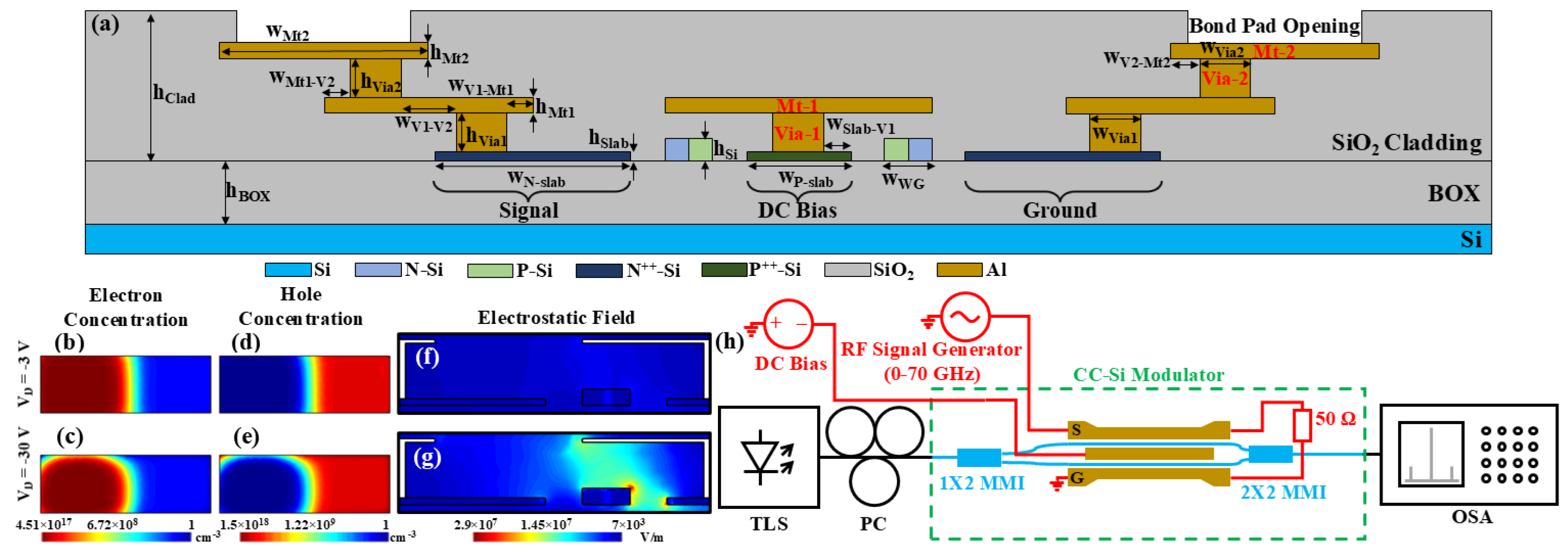
2. Device Structure
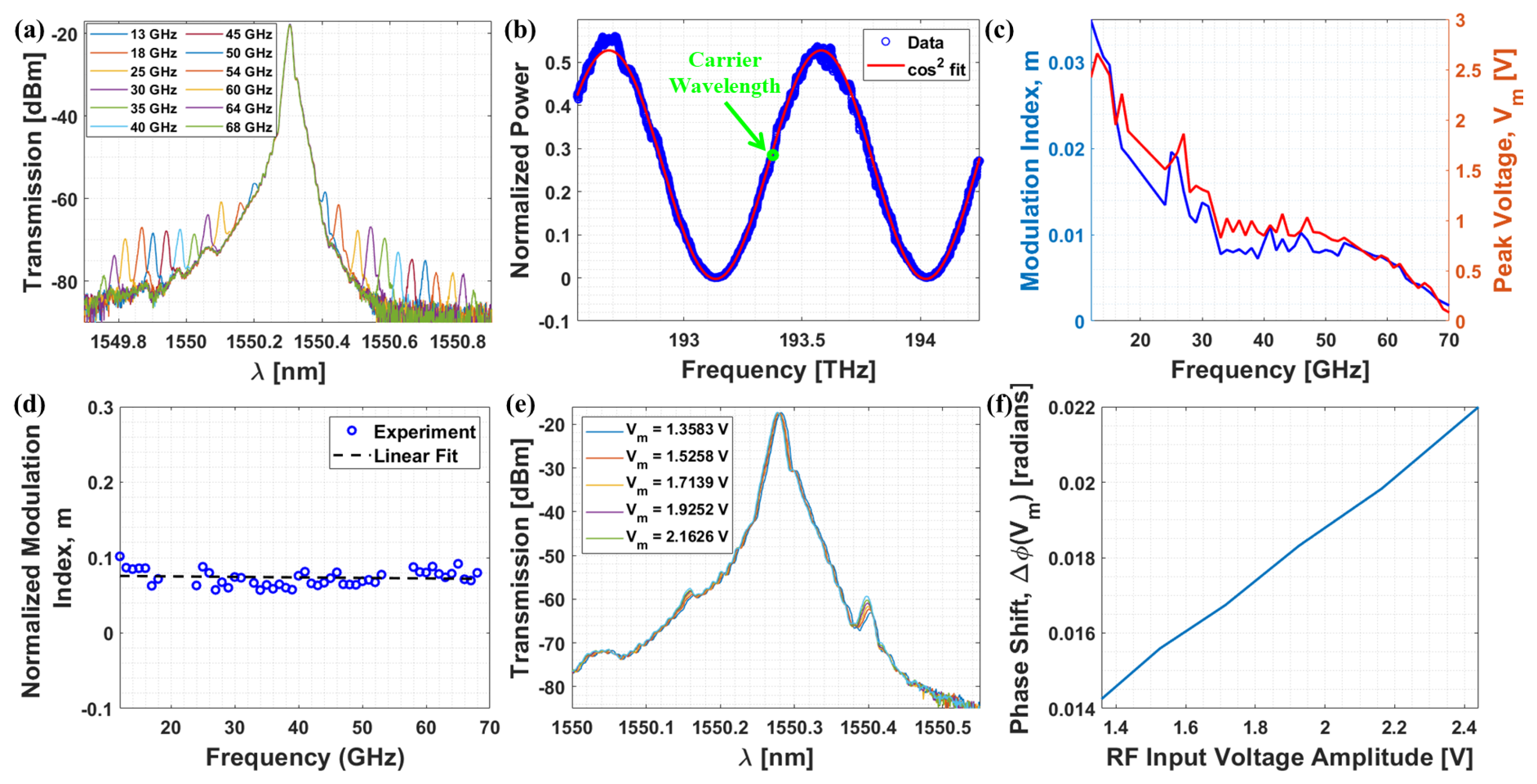
3. Experimental Demonstration
4. Conclusions
Author Contributions
Funding
Institutional Review Board Statement
Informed Consent Statement
Data Availability Statement
Acknowledgments
Conflicts of Interest
Abbreviations
| RC | Resistance–capacitance |
| SPP | Series push–pull |
| RF | Radio frequency |
| CMOS | Complementary metal-oxide semiconductor |
| PN | P-type/N-Type |
| TWE | Traveling wave electrode |
| CC-Si | Capacitively coupled silicon |
| MZI | Mach–Zehnder interferometer |
| MPW | Multi-project wafer |
| AMF | Advanced Micro Foundry |
| EO | Electro-optic |
| CW | Continuous wave |
| BOX | Buried oxide |
| TE | Transverse electric |
| DC | Direct current |
| PML | Perfectly matched layer |
| GS | Ground–Signal |
| TLS | Tunable laser source |
| PC | Polarization controller |
| PDK | Process design kit |
| MMI | Multimode interference |
| OSA | Optical spectrum analyzer |
| LNOI | Lithium niobate on insulator |
| BEOL | Back-end-of-line |
References
- Barnoski, M. Fundamentals of Optical Fiber Communications; Elsevier: Amsterdam, The Netherlands, 2012. [Google Scholar]
- Dong, P.; Lee, J.; Chen, Y.K.; Buhl, L.L.; Chandrasekhar, S.; Sinsky, J.H.; Kim, K. Four-channel 100-Gb/s per channel discrete multi-tone modulation using silicon photonic integrated circuits. In Proceedings of the 2015 Optical Fiber Communications Conference and Exhibition (OFC), Los Angeles, CA, USA, 22–26 March 2015; pp. 1–3. [Google Scholar] [CrossRef]
- Xie, C.; Magill, P.; Li, D.; Zhang, Y.; Zheng, L.; Wang, A.; Bao, Y.; Sui, C.; Streshinsky, M.; Mu, J.; et al. Real-Time Demonstration of Silicon-Photonics-Based QSFP-DD 400GBASE-DR4 Transceivers for Datacenter Applications. In Proceedings of the 2020 Optical Fiber Communications Conference and Exhibition (OFC), San Diego, CA, USA, 8–12 March 2020; pp. 1–3. [Google Scholar] [CrossRef]
- Yu, H.; Patel, D.; Liu, W.; Malinge, Y.; Doussiere, P.; Lin, W.; Gupta, S.; Narayanan, K.; Hoshino, I.; Bresnehan, M.; et al. 800 Gbps Fully Integrated Silicon Photonics Transmitter for Data Center Applications. In Proceedings of the 2022 Optical Fiber Communications Conference and Exhibition (OFC), San Diego, CA, USA, 6–10 March 2022; pp. 1–3. [Google Scholar] [CrossRef]
- Liao, L.; Liu, A.; Rubin, D.; Basak, J.; Chetrit, Y.; Nguyen, H.; Cohen, R.; Izhaky, N.; Paniccia, M. 40 Gbit/s silicon optical modulator for high-speed applications. Electron. Lett. 2007, 43, 1196–1197. [Google Scholar] [CrossRef]
- Watts, M.R.; Zortman, W.A.; Trotter, D.C.; Young, R.W.; Lentine, A.L. Low-Voltage, Compact, Depletion-Mode, Silicon Mach–Zehnder Modulator. IEEE J. Sel. Top. Quantum Electron. 2010, 16, 159–164. [Google Scholar] [CrossRef]
- Zhang, H.; Li, M.; Zhang, Y.; Zhang, D.; Liao, Q.; He, J.; Hu, S.; Zhang, B.; Wang, L.; Xiao, X.; et al. 800 Gbit/s transmission over 1 km single-mode fiber using a four-channel silicon photonic transmitter. Photon. Res. 2020, 8, 1776–1782. [Google Scholar] [CrossRef]
- Mohammadi, A.; Zheng, Z.; Lin, J.; Rad, M.M.; Zhang, X.; Rusch, L.A.; Shi, W. Segmented Silicon Photonic Modulator with a 67-GHz Bandwidth for High-Speed Signaling. In Proceedings of the Optical Fiber Communication Conference (OFC), San Diego, CA, USA, 6–10 March 2022; Optica Publishing Group: Washington, DC, USA, 2022; p. Th3C.1. [Google Scholar] [CrossRef]
- Han, C.; Zheng, Z.; Shu, H.; Jin, M.; Qin, J.; Chen, R.; Tao, Y.; Shen, B.; Bai, B.; Yang, F.; et al. Slow-light silicon modulator with 110-GHz bandwidth. Sci. Adv. 2023, 9, eadi5339. [Google Scholar] [CrossRef] [PubMed]
- Alam, A.S.; Sun, H.; Masnad, M.; Alamgir, I.; Azana, J.; Aitchison, J.S. Carrier Dispersion Modulation in a Silicon Strip Waveguide. In Proceedings of the CLEO 2024, Charlotte, NC, USA, 5–10 May 2024; Optica Publishing Group: Washington, DC, USA, 2024; p. JTh2A.195. [Google Scholar] [CrossRef]
- Alam, A.S.; Sun, H.; Poon, J.K.S.; Azaña, J.; Aitchison, J.S. Capacitively Coupled Silicon Modulator Fabricated on the Standard Silicon-on-Insulator Platform. IEEE Photonics J. 2025, 17, 3000208. [Google Scholar] [CrossRef]
- Shi, Y.; Yan, L.; Willner, A. High-speed electrooptic modulator characterization using optical spectrum analysis. J. Light. Technol. 2003, 21, 2358–2367. [Google Scholar] [CrossRef]
- Reynard, J.; Verove, C.; Sabouret, E.; Motte, P.; Descouts, B.; Chaton, C.; Michailos, J.; Barla, K. Integration of fluorine-doped silicon oxide in copper pilot line for 0.12-µm technology. Microelectron. Eng. 2002, 60, 113–118. [Google Scholar] [CrossRef]
- Alfaraj, N.; Lin, C.C.C.; Nasif, S.; Rajput, S.; Helmy, A.S. Facile integration of electro-optic SiO2/ITO heterointerfaces in MIS structures for CMOS-compatible plasmonic waveguide modulation. Light Adv. Manuf. 2023, 4, 420. [Google Scholar] [CrossRef]
- Alam, A.S. Design, Fabrication and Characterization of Capacitively Coupled Silicon-Organic Hybrid Modulators. Master’s Thesis, Karlsruhe Institute of Technology (KIT), Karlsruhe, Germany, 2017. [Google Scholar] [CrossRef]
- Ummethala, S.; Kemal, J.N.; Alam, A.S.; Lauermann, M.; Kuzmin, A.; Kutuvantavida, Y.; Nandam, S.H.; Hahn, L.; Elder, D.L.; Dalton, L.R.; et al. Hybrid electro-optic modulator combining silicon photonic slot waveguides with high-k radio-frequency slotlines. Optica 2021, 8, 511–519. [Google Scholar] [CrossRef]
- Ummethala, S. Plasmonic-Organic and Silicon-Organic Hybrid Modulators for High-Speed Signal Processing. Ph.D. Thesis, Karlsruhe Institute of Technology (KIT), Karlsruhe, Germany, 2021. [Google Scholar] [CrossRef]
- Alam, A.S.; Aitchison, J.S. Low Half-Wave-Voltage Lithium Niobate Modulator Using High-K Dielectric Material Cladding. In Proceedings of the Optica Advanced Photonics Congress 2022, Maastricht, The Netherlands, 24–28 July 2022; Optica Publishing Group: Washington, DC, USA, 2022; p. JTu2A.9. [Google Scholar] [CrossRef]
- Alam, A.S.; Aitchison, J.S. Optimization of a Broadband Lithium Niobate-Barium Titanate Hybrid Modulator with Low Half-Wave-Voltage-Length Product. IEEE Photonics J. 2023, 15, 6602407. [Google Scholar] [CrossRef]
- Chen, N.; Lou, K.; Yu, Y.; He, X.; Chu, T. High-Efficiency Electro-Optic Modulator on Thin-Film Lithium Niobate with High-Permittivity Cladding. Laser Photonics Rev. 2023, 17, 2200927. [Google Scholar] [CrossRef]
Disclaimer/Publisher’s Note: The statements, opinions and data contained in all publications are solely those of the individual author(s) and contributor(s) and not of MDPI and/or the editor(s). MDPI and/or the editor(s) disclaim responsibility for any injury to people or property resulting from any ideas, methods, instructions or products referred to in the content. |
© 2025 by the authors. Licensee MDPI, Basel, Switzerland. This article is an open access article distributed under the terms and conditions of the Creative Commons Attribution (CC BY) license (https://creativecommons.org/licenses/by/4.0/).
Share and Cite
Alam, A.S.; Nasif, S.; Aitchison, J.S. High-Bandwidth Silicon Strip Waveguide-Based Electro-Optical Modulator in Series Push–Pull Configuration. Photonics 2025, 12, 484. https://doi.org/10.3390/photonics12050484
Alam AS, Nasif S, Aitchison JS. High-Bandwidth Silicon Strip Waveguide-Based Electro-Optical Modulator in Series Push–Pull Configuration. Photonics. 2025; 12(5):484. https://doi.org/10.3390/photonics12050484
Chicago/Turabian StyleAlam, Ahmed Shariful, Sherif Nasif, and J. Stewart Aitchison. 2025. "High-Bandwidth Silicon Strip Waveguide-Based Electro-Optical Modulator in Series Push–Pull Configuration" Photonics 12, no. 5: 484. https://doi.org/10.3390/photonics12050484
APA StyleAlam, A. S., Nasif, S., & Aitchison, J. S. (2025). High-Bandwidth Silicon Strip Waveguide-Based Electro-Optical Modulator in Series Push–Pull Configuration. Photonics, 12(5), 484. https://doi.org/10.3390/photonics12050484