1. Introduction
In the 5G era, the global interconnection bandwidth has undergone exponential growth driven by advancements in cloud computing, the Internet of Things (IOT), and virtual/augmented reality (VR/AR) [
1]. As 6G approaches, technologies such as immersive cloud extended reality (XR), holographic communication, and sensory interconnection are expected to become mainstream applications [
2,
3,
4], which will lead to explosive growth in the data volume once again. Enhancing the transmission rate of devices and modules remains the primary challenge for future communication networks.
Electro-optic (E-O) modulators, functioning as pivotal components of optical transceivers in data centers, exhibit bandwidth characteristics that critically determine the transmission speed and signal fidelity of the system [
5]. Over the decades, modulators have been developed on various material platforms, such as group III-V compounds [
6], silicon [
7,
8,
9], and lithium niobate (linear E-O crystal) [
10,
11,
12]. Lithium niobate (LiNbO
3) has been extensively utilized in optical communication devices due to its excellent material properties, such as the linear E-O effect (Pockels effect), its large E-O coefficient, its wide transparent window (ranging from 350 nm to 5 μm), and its low optical absorption loss. Traditional bulk-material LiNbO
3 modulators, which rely on diffused planar waveguide structures, suffer from limitations, such as large size, low modulation rates, and poor integration [
13], rendering them inadequate to meet the demand of the rapidly developing communication capacity. In recent years, waveguides fabricated on thin-film lithium niobate (TFLN) have exhibited a large refractive index difference and a nanoscale size, making it possible to implement modulators with a large bandwidth, low loss, and high integration.
High-speed modulators utilize the transmission line, specifically traveling-wave electrodes (TWEs), to guide RF signals to transmit in the same direction as the optical carrier. This design enables a higher modulation rate and broader E-O bandwidth. Coplanar waveguides (CPWs), with significant advantages, including low loss, low dispersion, and a simple structure, are commonly used in RF-integrated circuits and optoelectronic chips. Most importantly, by placing optical waveguides (such as silicon and LiNbO3) within the metal gaps of a CPW, RF signals can achieve dual push–pull modulation on the optical carriers on both sides. This configuration significantly reduces the half-wave voltage and power consumption of modulators and has great application value in high-speed digital communication.
The velocity mismatch, characterized by the refractive index difference (Δn) between RF signals and optical carriers, is the main factor limiting the bandwidth of E-O modulators. As the Δn or the signal frequency increases, the E-O response deteriorates significantly. Therefore, precise velocity matching is of great significance for expanding the E-O bandwidth to higher frequency bands (>100 GHz). The refractive index of optical carriers (n
oc) on a chip is primarily determined by the materials and morphologies of the optical waveguides and the cladding, which are difficult to adjust during fabrication. Additionally, it remains difficult to adjust the RF refractive index (n
RF) by changing the dimensions of the CPW electrode, such as the width of the signal line or the width of the gaps at the chip scale. Fortunately, slow-wave structures (SWSs), such as a series of micro-structures with specific shapes, can be loaded onto a uniform transmission line individually or periodically, changing the reactance characteristics and, ultimately, reducing the microwave velocity. Compared with an unloaded transmission line, SWSs can achieve a wider range of velocity adjustments and have been successfully applied in terahertz traveling-wave tubes (TWTs) [
14,
15] and millimeter-wave antennas [
16,
17]. Likewise, electrodes loaded with SWSs can more readily achieve the matching between the n
RF and n
oc. In recent years, numerous reported broadband TFLN modulators have ameliorated the velocity mismatch on chips with the aid of CPW electrodes periodically loading slots or T-shaped stubs [
18,
19,
20]. However, there are scarcely any works that have accommodated velocity matching, impedance matching, fabrication efficiency, and costs.
In this paper, we utilized a CPW electrode co-loaded with square serrations and T-shaped stubs to simultaneously achieve outstanding velocity matching and impedance matching. Through the ultraviolet lithography processes, we successfully fabricated an E-O modulator chip with a bandwidth far exceeding 67 GHz and a return loss of greater than 12 dB on a silicon-based TFLN platform. In addition, we analyzed the mechanism of double slow-wave structures at the simulation level, providing valuable insights for regulating the velocity of RF signals in an electrode.
2. Design and Simulations
The overall design of the broadband modulator is illustrated in
Figure 1a. The optical section employs the classic Mach–Zehnder structure: An optical carrier is equally divided into two beams by a multimode interference coupler (MMI), which then propagates through two modulation arms. After passing through the E-O modulation region, they are combined again by another MMI. The input and output of the optical carrier are located on the same side, enabling a higher integration density and suitability for applications in multi-channel modulator arrays and modules. RF signals are transmitted in the RF electrode loaded with an SWS, and the electric field is concentrated in the gaps where the optical waveguide is located, enabling efficient E-O modulation. A nickel–chromium (NiCr) alloy thermal resistor is placed near the modulation arm, and it is powered by a DC-bias electrode to generate Joule heat. Through the thermo-optical effect, a more compact device size and more stable bias control can be achieved [
21].
Figure 1b shows the cross-sectional structure of the E-O modulation region. The substrate is high-resistivity silicon, and the E-O crystal layer is TFLN with a thickness of 600 nm. The buried oxide layer has a thickness of 4.7 μm. The ridge waveguides are formed by etching the TFLN layer, and the height of the ridges is 300 nm. The RF electrode loaded with the SWS (slow-wave electrode) is fabricated from gold and deposited on the slab of TFLN after etching in the E-O modulation region. The thickness of the electrode simultaneously affects the RF characteristics and modulation efficiency of the device. Based on the simulation analysis, it can be concluded that both the transmission loss and characteristic impedance of the CPW decrease with an increase in the conductor thickness. The characteristic impedance exhibits a gradual progression with an increase in the conductor thickness, and the transmission loss approaches a plateau when the thickness exceeds 800 nm. However, the overlap area between the electric field and optical field should be maximized to enhance the modulation efficiency of the device; thus, the conductor thickness cannot be excessive for a 300 nm high LN ridge waveguide. Finally, the electrode thickness is determined to be 900 nm.
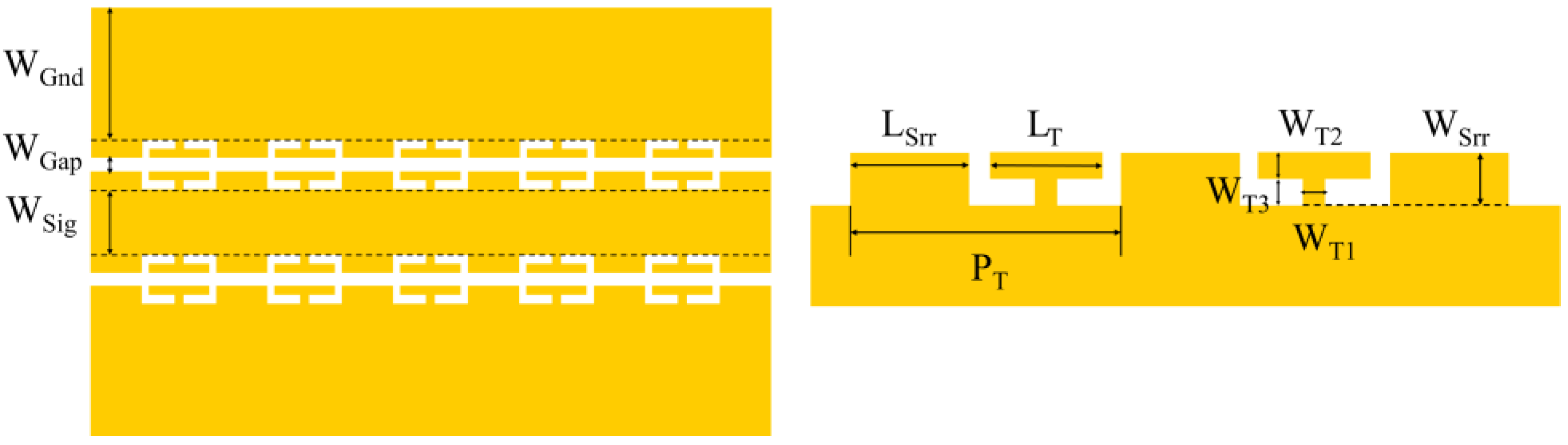
Figure 2 shows the schematic structure of the slow-wave electrode. In order to minimize the ohmic loss, the signal line width (W
Sig) is 20 μm before loading the SWS, while the ground line width (W
Gnd) is 180 μm. Periodically arranged square serrations and T-shaped stubs extend from the sides of the signal line and the ground lines. The width of the square serration W
Srr is equal to the sum of the W
T2 and W
T3, which is the total width of the stub. The sum of the serration length L
Srr and the stub length L
T is a constant value close to the period length P
T. Consequently, new conductor gaps are formed between the slow-wave structures. The modulation efficiency of the device increases as the conductor gap width W
Gap decreases, while the RF transmission loss simultaneously rises. Moreover, an excessively small W
Gap would induce strong metal absorption and significant optical attenuation. For TFLN modulators, the gap width of the electrode typically ranges between 5 and 7 μm. Comprehensively considering the fabrication quality combined with broadband performance requirements, W
Gap is preferentially selected as 7 μm. The cut-off frequency f
c of the first passband in a periodically loaded transmission line is given by Equation (1), where L
s and C
s, respectively, represent the lumped inductance and capacitance per unit period, approximately correlated with P
T. A larger P
T would result in a lower f
c, thereby limiting the device’s high-frequency performance. Furthermore, since the gaps between adjacent SWSs may weaken the E-O interaction in those regions, the total length of the SWS (L
Srr + L
T) within each period should be maximized to approach the P
T as closely as the fabrication tolerances permit. Therefore, they are set to P
T = 50 μm and L
Srr + L
T = 45 μm in this design. Moreover, W
T1, W
T2, and W
T3 are set to the minimum processable length of 2 μm (W
Srr is 4 μm) in order to make the stubs more tunable and the electrode more compact, simultaneously. The length of the complete slow-wave electrode in the E-O modulation region is 8 mm to balance the RF loss and the half-wave voltage.
According to the transmission line theory [
22], the electrical characteristics of a TWE can be analyzed and characterized through a distributed-parameters network in the millimeter-wave band. As a non-uniform transmission line, a slow-wave electrode lacks inherent distributed parameters due to its spatially varying geometrical dimensions and heterogeneous structural configurations along the signal propagation axis. However, since the dimensions and the periodic length of the loaded SWS are significantly smaller than the millimeter-wave wavelength, the slow-wave electrode can still be approximately regarded as a uniform transmission line with effective electromagnetic properties [
23].
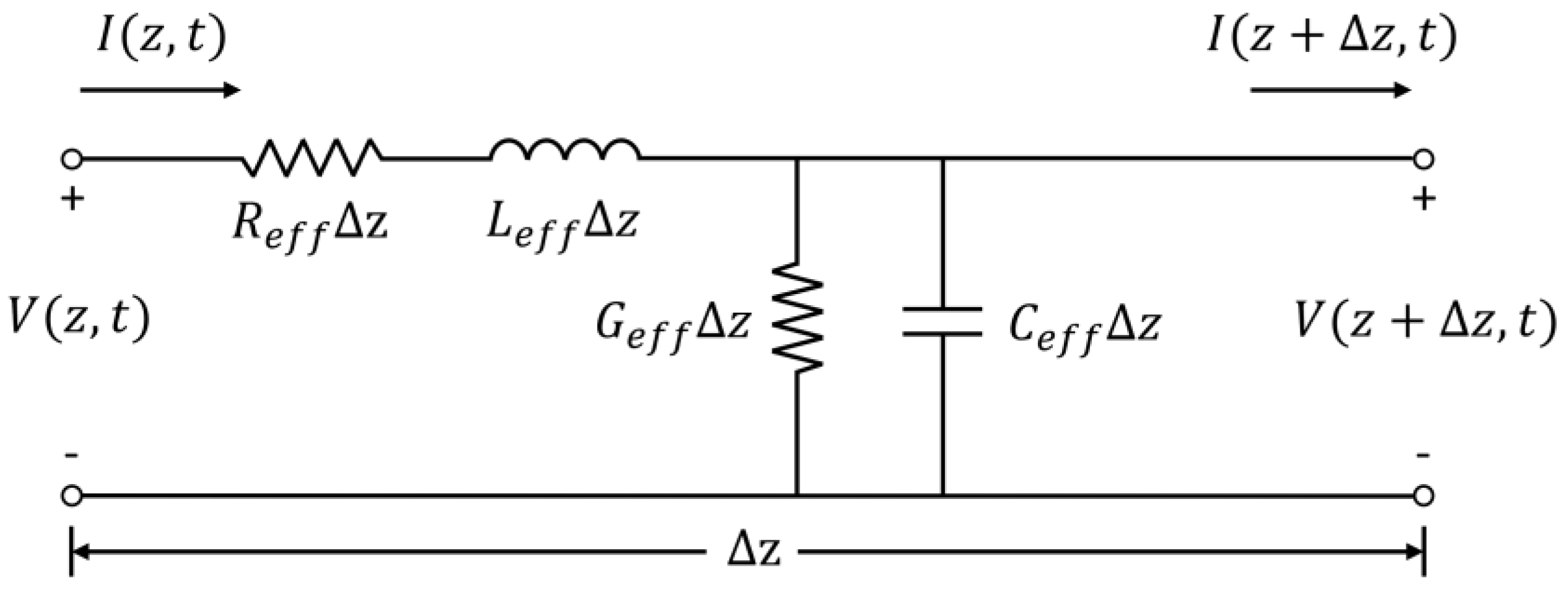
Figure 3 shows the equivalent circuit model of a slow-wave electrode per unit length (
), where R
eff, L
eff, G
eff, and C
eff represent the effective distributed resistance, inductance, conductance, and capacitance, respectively. Under the high-frequency and low-loss approximation, the n
RF and effective characteristic impedance Z
eff of slow-wave electrodes can be expressed by Equation (2).
The finite element method (FEM) in the frequency domain is used to simulate slow-wave electrodes with a total length of 1 mm (20 periods), where L
T is regarded as the sole independent variable. The required electrical indicators of the electrodes are obtained by analyzing information such as the amplitude and phase of the scattering parameters (S-parameters) within the wide frequency band. Particularly, the n
RF can be calculated from the S
21-phase transmission curve by the following equation:
where v
RF is the phase velocity of the RF signals, β is the phase constant of the electrode, f is the RF frequency, ω is the angular frequency, φ (in radians) is the phase shift of the RF signals at each frequency, and L is the phase shift length.
Figure 4a shows the simulated Z
eff and n
RF of the electrode corresponding to different values of L
T. As the L
T increases from 5 μm to 40 μm, the Z
eff gradually increases from 45 Ω to 50 Ω. Meanwhile, the n
RF of the slow-wave electrodes increases from 2.238 to 2.496 and is always greater than the n
RF of the regular electrode without an SWS, which is 2.14. The L
eff and C
eff can be calculated by Equation (4) and are shown in
Figure 4b. Compared with the regular electrode, the C
eff increases significantly from 120.7 fF/mm to approximately 165 fF/mm, while the L
eff decreases correspondingly with the length of the SWS. This is because the square serrations can be regarded as shunt inductors, which play a role in reducing the distributed inductance of the transmission line. When the L
T increases (and the L
Srr decreases), the C
eff stabilizes, while the L
eff exhibits linear growth and approaches the distributed inductance of the regular electrode, which is 424.6 pH/mm. The f
c of the designed slow-wave electrode can be approximately calculated to be 800 GHz with Equation (1), where
Ls ≈ PTLeff and
Cs ≈ PTCeff. This indicates that the slow-wave electrodes possess a sufficiently wide passband to support the transmission of RF signals.
3. Fabrication and Results
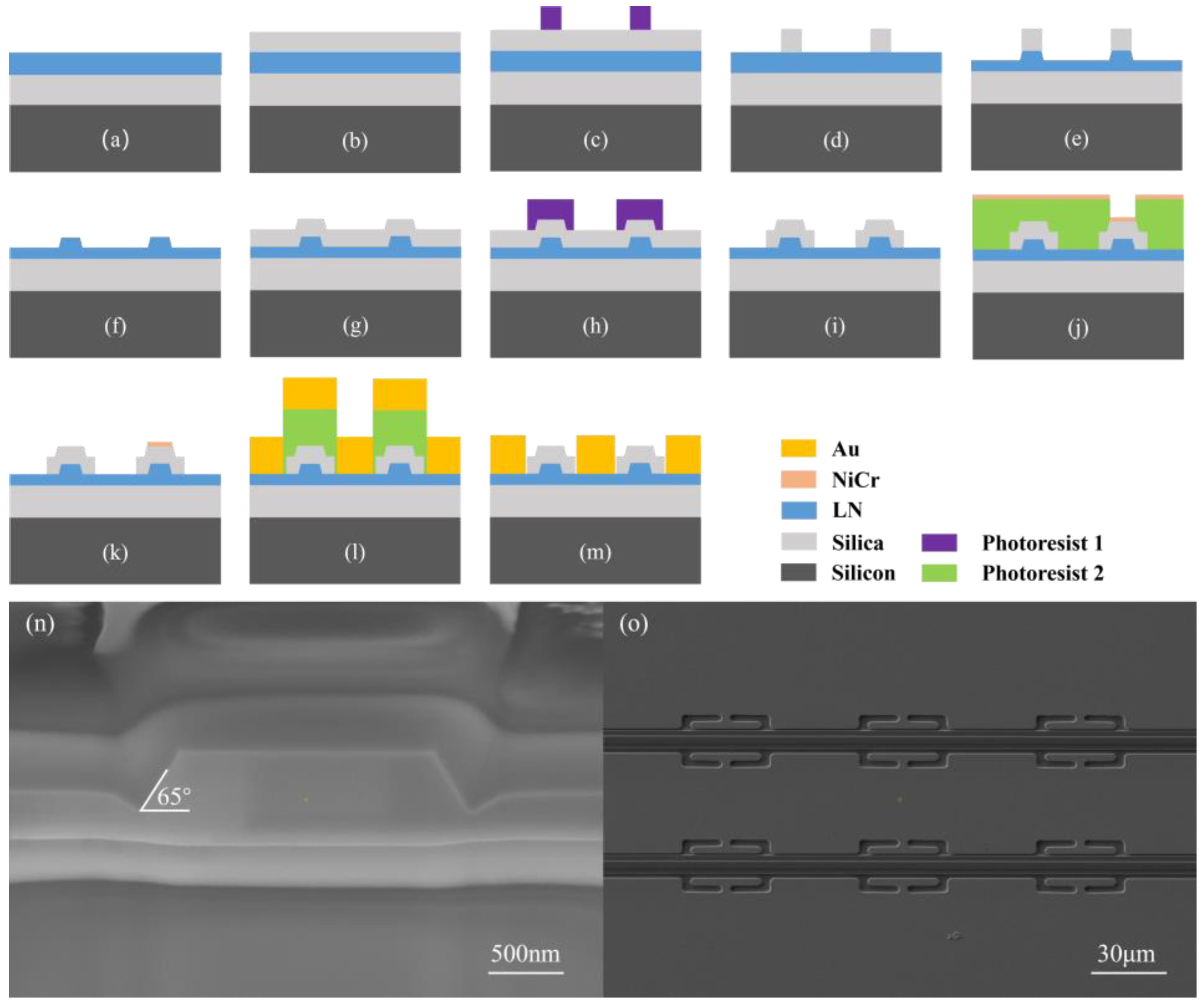
The modulator chips were fabricated on X-cut LNOI wafers (NANOLN), and the fabrication processes are shown in
Figure 5a–m. All the patterning processes were performed using traditional ultraviolet (UV) lithography. This enabled us to pattern the structure at a faster speed and lower cost compared with electron-beam lithography (EBL) while maintaining good alignment accuracy. A thick silica layer was used as the hard mask for the TFLN layer. After patterning, the LiNbO
3 ridge waveguides were fabricated by inductively coupled plasma reactive-ion etching (ICP-RIE) with an etching depth of 300 nm. After removing the remaining mask with the buffered oxide etch (BOE) solution, a silica buffer layer with a thickness of 900 nm was deposited again on the entire chip. The buffer could both confine the optical carrier within the LiNbO
3 waveguide and prevent severe optical loss caused by metal absorption in the area where the electrode overlapped with the waveguide. Subsequently, the buffer in the E-O modulation region was removed through ultraviolet lithography and dry etching. Most of the lattice defects introduced by previous etching processes were removed through annealing, which could reduce the on-chip optical loss. The NiCr thermal resistance near the ridge waveguide was fabricated by ultraviolet lithography, electron-beam evaporation, and the lift-off process. The gold electrode co-loaded with square serrations and T-shaped stubs was prepared in the same way. It should be clarified that
Figure 5l,m show the fabrication process of slow-wave electrodes within the modulation region, and the NiCr resistor shown in
Figure 5j,k was fabricated outside the region, but it was securely clamped by the gold DC electrode to establish the electrical connectivity shown in
Figure 1a.
Figure 5n,o present the TFLN ridge waveguide and slow-wave structures photographed under a scanning electron microscope, respectively. The ridge waveguide with smooth sidewalls had a width of 1.5 μm and an inclination angle of 65°. The serrations and stubs on the electrode feature precise dimensions and a well-defined morphology.
For RF characterization, a pair of RF probes were respectively inserted into the pads of the electrodes and connected to the ports of a vector network analyzer (VNA). The model of the VNA we used was Keysight N5227B (Keysight, Santa Rosa, CA, USA), with a measurement range of 0.01–67 GHz.
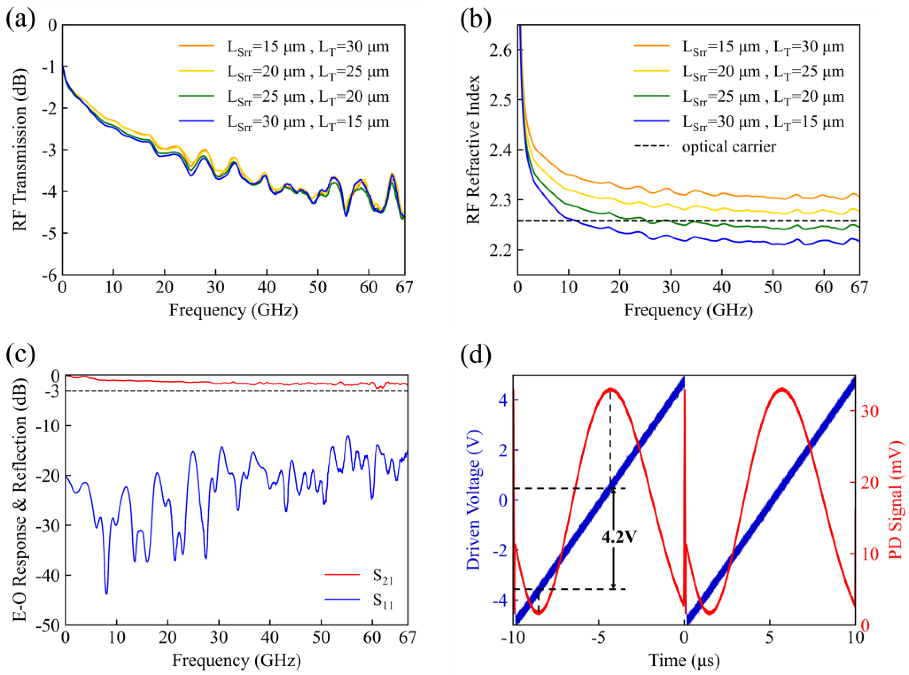
Figure 6a shows the RF transmission (S
21-power transmission) curves of the electrodes loaded with SWSs of different lengths. From 0.01 to 67 GHz, all the transmission curves exhibit a roll-off of approximately 3.6 dB, showing no significant difference in the transmission loss with the increase in the L
T due to the slight variation in the effective distributed resistance (R
eff), effective distributed conductance (G
eff), and Z
eff according to Equation (5), where the α is the attenuation constant of the slow-wave electrode.
Figure 6b shows the measured n
RF of the slow-wave electrodes, which, indeed, demonstrates an upward trend with the increment in the L
T. As for the electrode with an SWS of L
Srr = 25 μm and L
T = 20 μm, the measured n
RF is approximately 2.245, precisely matching with the n
oc, which is 2.258. However, it should be noted that all the measured n
RF values are roughly 0.1 lower than the simulation results, which indicates that there is a problem of low distributed capacitance (or distributed inductance) in the gold electrodes due to the fabricated processes.
Finally, a modulator with an SWS of L
Srr = 25 μm and L
T = 20 μm was selected and coupled with a dual-channel fiber array (FA) for E-O response measurements at 1550 nm. An external 50-Ω-terminator was connected at the end of the RF electrode to absorb electromagnetic energy and prevent signal reflection. The normalized E-O response and electrode reflection of the modulator is shown in
Figure 6c. Within the range of 0.01–67 GHz, the S
11-power reflection curve remains below −12 dB, which indicates that the impedance of the device was well-matched with the external RF system. The E-O bandwidth of modulators is typically defined as the frequency at which the E-O response rolls off by 3 dB from its low-frequency value in engineering. Accordingly, the E-O bandwidth of this modulator chip far exceeds 67 GHz, since most of the S
21-power transmission curve is above −2 dB, except for a dip at 60.5–62 GHz, which reaches −2.5 dB. It should be emphasized that the dip is introduced by external factors of the chip and does not disrupt the gentle downward trend of the curve.
The half-wave voltage (V
π) is defined as the critical driving voltage to induce a π-phase shift that modulates the optical output intensity from the maximum to minimum value. The product of this voltage and the modulation length (V
π⋅L) serves as a key metric for characterizing the device’s modulation efficiency. The V
π of our modulator chip was measured through the triangular wave method.
Figure 6d shows the 100 kHz input signals (blue curve, V
pp = 10 V) and the output signals (red curve), yielding a V
π = 4.2 V for the 8 mm length modulation region and corresponding to V
π⋅L = 3.36 V·cm.
4. Discussion
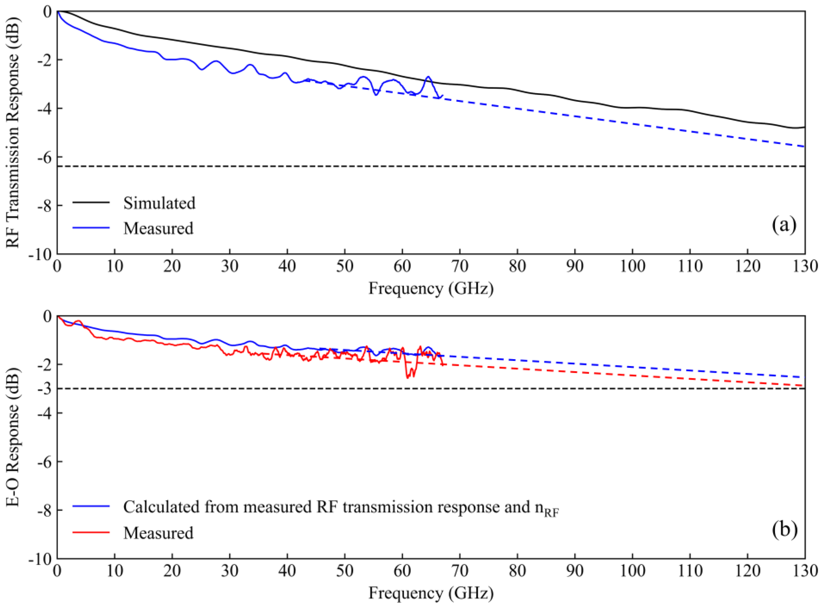
Due to the limited testing range of the equipment, the 3 dB bandwidth of the modulator chip could not be directly obtained. Therefore, the test curves were extrapolated and extended following specific principles. The black curve in
Figure 7a shows the simulated RF transmission response of a slow-wave electrode within 0–130 GHz, exhibiting a roll-off rate in the high-frequency region of approximately 0.029 dB/GHz. Accordingly, a linear extrapolation could be applied to the measured RF transmission response (blue curve) based on the simulated curve. Assuming no RF signal reflection in the electrode, the E-O response could be approximately expressed by Equation (5) [
24], where ξ represents the velocity mismatch degree of the modulator, and αL is the transmission loss of an electrode. The blue curve in
Figure 7b depicts the calculated E-O response using the measured RF transmission response and n
RF, while the red curve shows the measured E-O response. Clearly, the measured E-O response aligns well with the calculated value. As the n
RF tends to stabilize in the high-frequency range, the calculated roll-off rate of the E-O response is approximately 0.0137 dB/GHz. Ultimately, the red curve reaches its −3 dB cutoff at 130 GHz, and this value can be roughly recorded as the 3 dB bandwidth of our fabricated modulator chip.
A comparison between the bandwidth performance of this device and other state-of-the-art works is presented in
Table 1. The TFLN modulator chip, designed and fabricated without any modification or processing of the silicon substrate, demonstrated an excellent electro-optic bandwidth. Furthermore, all patterning processes of the chip were accomplished through UV lithography, and the electrode was fabricated with merely a single lithography step and a metal lift-off process. This solution offers the advantages of low process complexity and manufacturing costs while simultaneously exhibiting potential for large-scale photonic integration.
For a 7 μm gap width, the measured V
π⋅L of the device was 3.36 V·cm. Since it does not fully exploit the excellent modulation efficiency of thin-film lithium niobate modulators, we propose to reduce the gap width to 5–6 μm in subsequent optimizations. This reduction in the gap width will lead to an increase in the microwave refractive index; therefore, the length of the slow-wave structures will need to be accordingly adjusted.

 ,
, 

