Article

Compact Four-Channel Optical Emission Module with High Gain

1
Institute of Semiconductors, Chinese Academy of Sciences, Beijing 100083, China
2
The College of Materials Science and Opto-Electronic Technology, University of Chinese Academy of Sciences, Beijing 100049, China
3
Institute of Intelligent Photonics, Nankai University, Tianjin 300071, China
*
Authors to whom correspondence should be addressed.
These authors contributed equally to this work.
Photonics 2025, 12(5), 425; https://doi.org/10.3390/photonics12050425
Submission received: 5 April 2025 / Revised: 25 April 2025 / Accepted: 27 April 2025 / Published: 28 April 2025
(This article belongs to the Special Issue Microwave Photonics: Science and Applications)

Abstract

:
In this paper, a four-channel optical emission module is developed using hybrid integration technology that integrates directly modulated laser (DML) chips, low-noise amplifier (LNA) chips, and control circuits, with dimensions of 24.4 mm × 21 mm × 5.9 mm. This module enables high-gain signal output and minimizes crosstalk between neighboring channels while improving integration. An equivalent circuit model of radio frequency (RF) signal transmission is established, and the accuracy of the model and the effectiveness of the approach to improve signal gain are verified using simulations and experiments. With optimized thermal management, the module has the ability to operate at stable temperatures across an ambient range of −55 °C to 75 °C. The module has a channel wavelength spacing of approximately 1 nm, and the −3 dB bandwidth of each channel exceeds 20 GHz. The crosstalk between neighboring channels is less than −65 dB. In the range of 0.8~25 GHz, the four-channel gain is approximately 15 dB through the integration of the LNA chip. The module achieves a noise figure (NF) of less than 30 dB.

1. Introduction

With the rapid development of the internet and the data communication industry, there is an urgent need to enhance communication rates and capacities [1,2]. Microwave photonics technology has emerged as a solution, with optical transceiver modules being one of its key elements. Optical transceiver modules enable electro-optical and photoelectric conversion, playing a crucial role in system applications such as radio over fiber (RoF) communications and radar systems [3,4,5]. Consequently, they need to evolve toward trends of integration, high gain, and high bandwidth [6,7].
Hybrid integration technology is a practical packaging approach to achieve high gain and module integration by assembling optical chips, electrical chips, and other components in a tube shell [8,9,10,11,12,13]. To achieve a compact package and simultaneously enhance the performance of the packaged module, researchers have conducted extensive studies. A three-dimensional radio-frequency (RF) impedance matching circuit was proposed by Z. Zhang et al. in 2016. The circuit effectively minimized module size, reduced heat accumulation, and decreased electrical crosstalk. The crosstalk between adjacent channels was below −30 dB across the direct current (DC) to 30 GHz range. A ten-channel optical emission module with a bandwidth of about 10 GHz was demonstrated using the packaging design [14]. In 2018, the Institute of Semiconductors of the Chinese Academy of Sciences adopted hybrid integration technology to integrate an arrayed waveguide grating (AWG) and directly modulated laser (DML) chips, achieving an ultra-compact four-channel optical emission module with dimensions of 11.5 mm × 5.4 mm × 5.4 mm. The measured −3 dB bandwidth of the four channels was 3 GHz. The electrical crosstalk was suppressed to below −23 dB from DC to 30 GHz [15]. In 2019, Z. Zhao et al. proposed a three-dimensional microwave circuit for compact packaging, with the signal traces and bias networks fabricated on individual circuit boards followed by vertical assembly. A four-channel optical receiver module measuring 23.3 mm × 6.0 mm × 6.5 mm was constructed based on the proposed microwave circuit [16]. In 2021, S. -J. Yun et al. presented a compact transmitter-receiver optical subassembly (TROSA) module. The transmitter integrates four DMLs on a silicon carrier, coupled to a vertically polished AWG through edge-aligned assembly, demonstrating stable operation against optical feedback. The receiver employs a 45° polished AWG for passive alignment with photodetectors (PDs). Both submodules were co-packaged into a housing measuring 25 mm × 15 mm × 6.4 mm. The measured −3 dB bandwidths for CH1 to CH4 were 29.1, 27.8, 28.1, and 28.8 GHz, respectively [17]. In 2024, a hybrid integrated silicon receiver module was demonstrated by Jin’s team et al. A four-channel vertical PD array and a four-channel transimpedance amplifier (TIA) were integrated in the packaging scheme. After electro-optical co-simulation and fabrication, the −3 dB bandwidth of the receiver was improved to over 48 GHz through TIA equalization [18].
For optical emission modules, conventional designs comprising only lasers generate weak signals with measured gains generally below −20 dB in practical testing [19], limiting their effectiveness in communication systems. In practical applications of optical emission modules, such as during system testing, optical or electrical signal amplification compensation is always required. However, using semiconductor optical amplifiers (SOAs) or erbium-doped fiber amplifiers (EDFAs) for optical amplification introduces significant noise figure (NF) and leads to increased system size [20,21]. In contrast to these optical amplification solutions, connecting a low-noise amplifier (LNA) at the front end of the optical emission module can reduce the impact of noise [22]. However, the issue of large system size persists. In addition, traditional optical emission modules often rely on external control circuits to ensure stable laser operation, which also results in an increased system size. Finally, the thermal management of the module remains an understudied aspect in current research.
Considering the current state of research and engineering application requirements, further research is required to improve the gain and integration level of the optical emission module without compromising thermal dissipation. In this paper, a four-channel optical emission module is designed and fabricated for optical phased array applications. Using hybrid integration technology, the module integrates DML chips, LNA chips, and control circuits, enabling higher component density. The module can realize the amplification of RF signals and electro-optical conversion while controlling the temperature of the laser chip in a compact size of only 24.4 mm × 21 mm × 5.9 mm. An equivalent circuit model of RF signal transmission is constructed; it enables the creation of a comprehensive optoelectronic simulation system for both photonic and electrical devices. Through simulation-optimized thermal management design, the module maintains its temperature below 30 °C across an ambient range of −55 °C to 75 °C, ensuring reliable operation. Furthermore, the simulation of the optical coupling scheme provides guidance for process tolerances in actual fabrication. The module operates stably under the control of the circuit, with a channel wavelength spacing of approximately 1 nm, matching the spacing of the antenna in practical applications. The −3 dB bandwidth of each channel exceeds 20 GHz. The crosstalk between neighboring channels is less than −65 dB in the compact structure. In the range of 0.8~25 GHz, the four-channel gain is approximately 15 dB through the integration of the LNA chip. The module exhibits a noise figure below 30 dB.
The following section outlines the structure of the paper. Firstly, the structural design of the four-channel optical emission module is presented in Section 2. Subsequently, simulation analysis is conducted in Section 3, including thermal simulation, optical simulation, optimized design of RF signal transmission lines, and the co-simulation of the optoelectronic chip. Then, the experimental results and discussion are presented in Section 4. Finally, conclusions are summarized in Section 5.

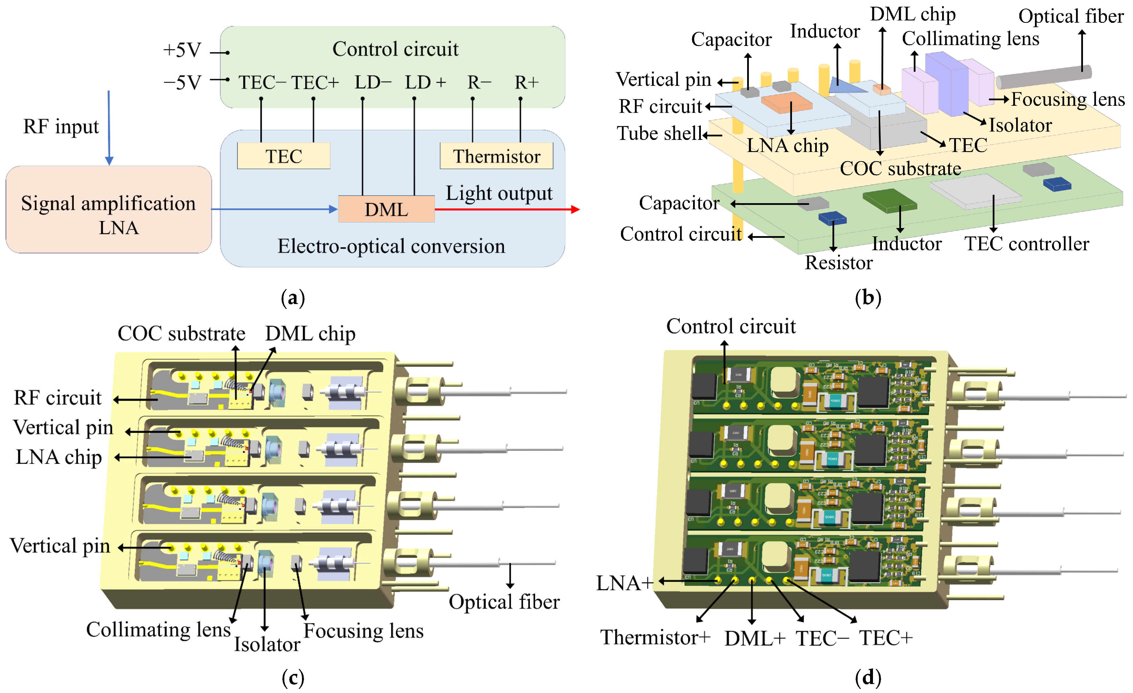
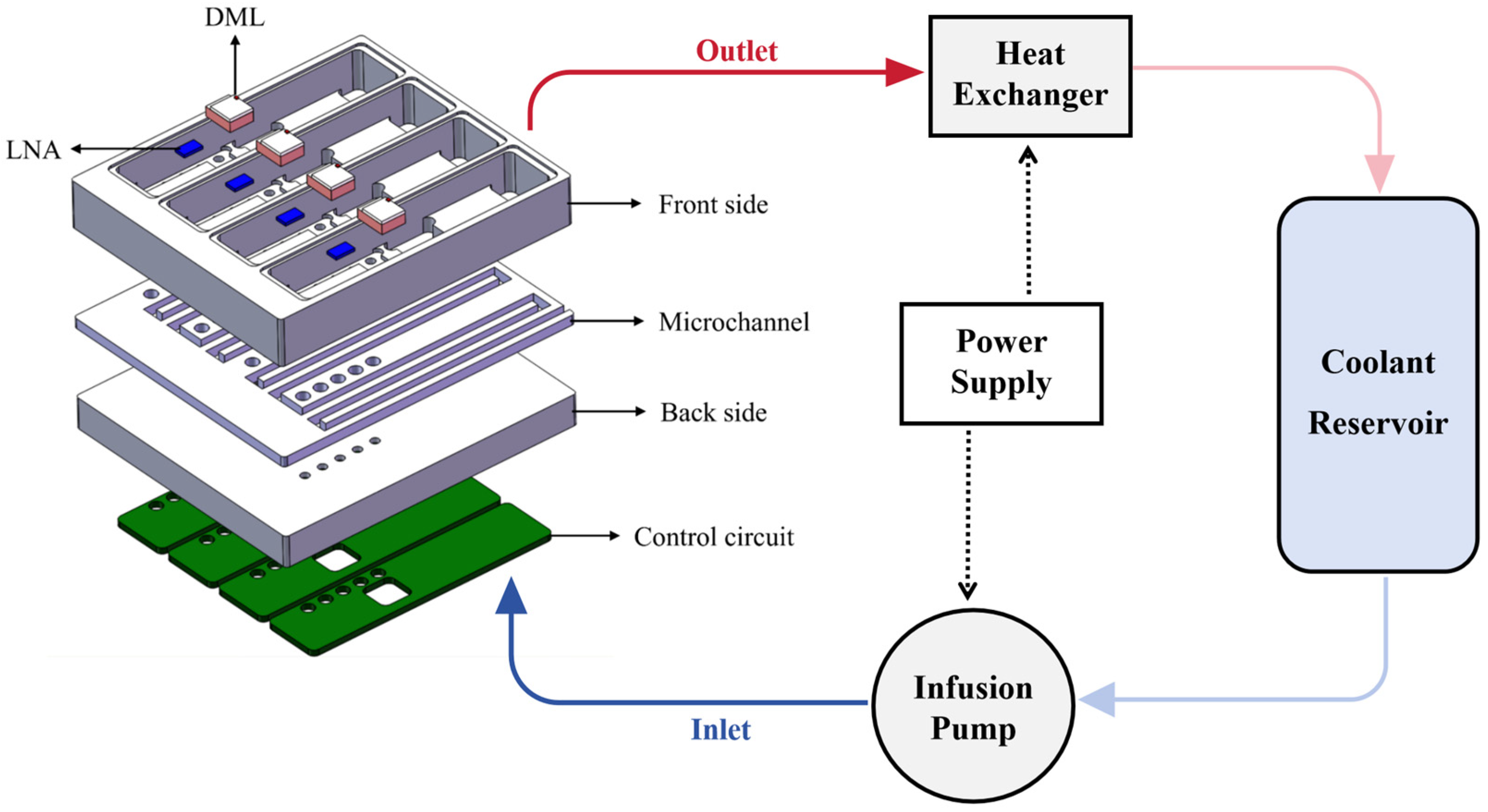
2. Device Structural Design

The four-channel high-gain integrated optical emission module is mainly composed of three core parts, including the signal amplification section, the control circuit, and the electro-optical conversion section, as shown in Figure 1a. The signal amplification section inputs the received RF signal into an LNA chip to amplify the signal. The control circuit includes temperature control to ensure the proper working environment for the optical chips. The electro-optical conversion section converts the RF signal into an optical signal through a DML chip and transmits the optical signal to the external part of the module using an optical fiber.
The four-channel module is separated into four chambers to reduce RF signal crosstalk. The conceptual design of the single chamber is shown in Figure 1b. Each chamber contains independent RF circuit, LNA chip, chip-on-carrier (COC) substrate, DML chip, optical coupling components, and so on. The input RF signal first passes through the RF circuit, which converts its transmission structure from a coaxial structure to a coplanar structure. After amplification by the LNA chip, the RF signal is transmitted through the COC substrate to the DML chip, where it is finally converted into an optical signal. The RF and the DC signal should be injected into the DML at the same time. The traditional scheme is to feed them together from the RF connector to the DML through an RF transmission line and a series matching resistor [23]. In this structure, the DC power through the series matching resistor will generate additional heat and power consumption. In addition, it is usually necessary to use a DC bias before the RF connector to adjust the RF signal and DC levels, which will have an impact on the module. The module in this paper uses an independent DC bias circuit consisting of a high-frequency inductor and capacitor that is placed between the series matching resistor and the DML chip, which will improve the above problems. After the electro-optical conversion through the DML chip, the laser beam diverges in both horizontal and vertical directions. Direct coupling with the optical fiber would result in low efficiency, so a coupling method involving a double lens and an isolator is adopted. To improve the integration of the module and simplify the test, the control circuit with a thermoelectric cooler (TEC) controller is integrated into the back of the tube shell. Vertical pins on the tube shell interconnect the electrodes on the front and back of the package, supplying voltage and current to the LNA chip, the DML chip, the TEC, and other components.
Figure 1c,d show the configuration of the optical emission module. On the front side of the package, the vertical pins and the electrodes of the chip or device are connected by gold wire bonding. On the back side of the package, the vertical pins are connected to the control circuit board by solder. As shown in Figure 1d, the vertical pins from left to right function as follows: voltage supply for the LNA chip, current injection for the thermistor, bias current supply for the DML chip, current path for the negative TEC terminal, and current path for the positive TEC terminal. The design size of the four-channel optical emission module is 24.4 mm × 21 mm × 5.9 mm.

3. Simulation Analysis

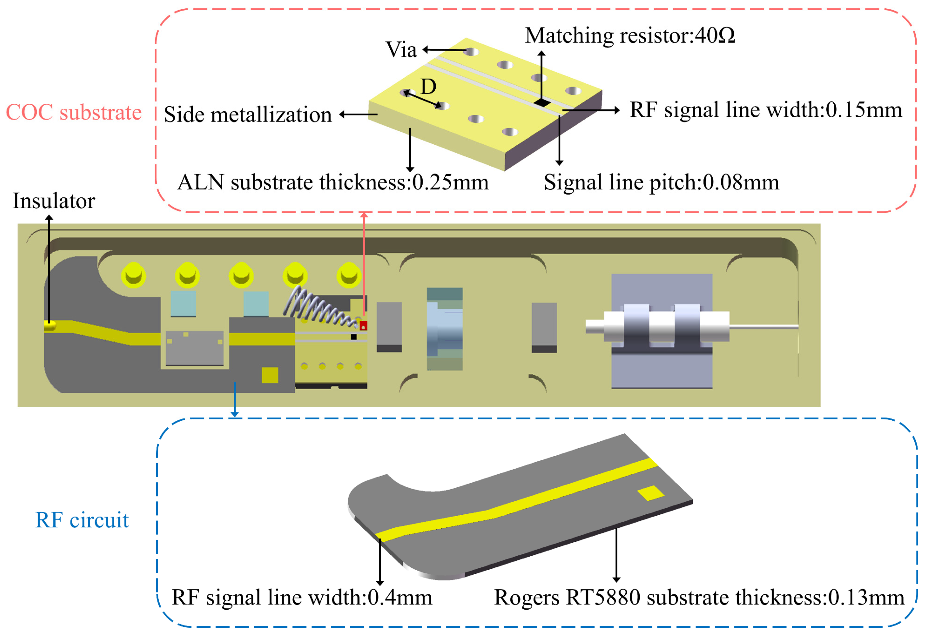
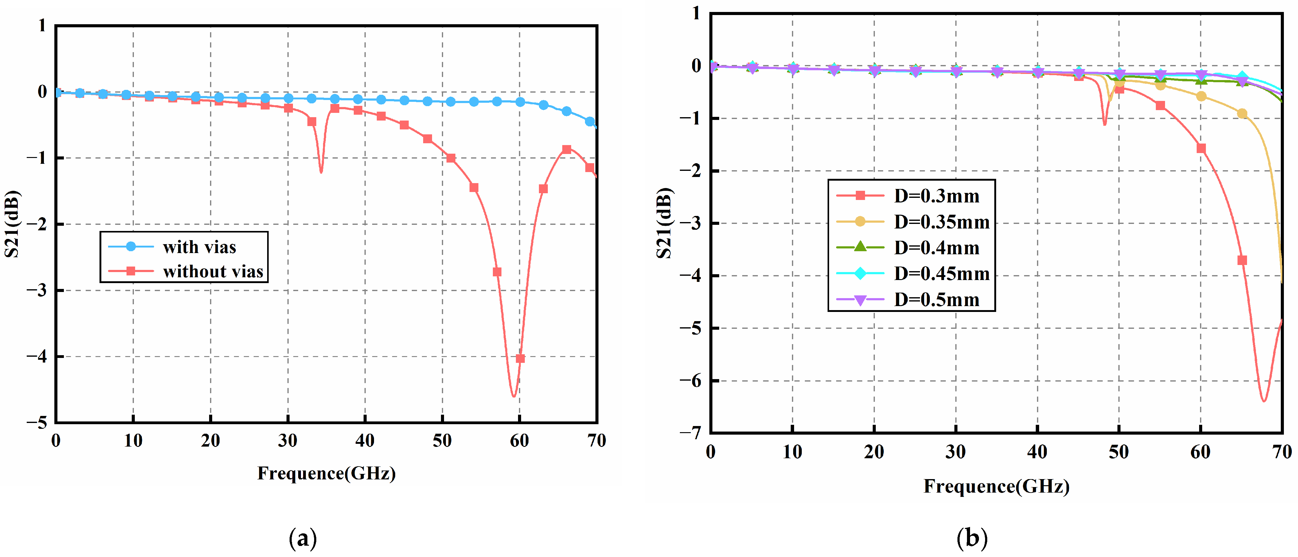
3.1. Transmission Line Simulation Design

To ensure the low loss transmission of the RF signal before it is injected into the DML chip, suitable transmission line structures must be designed. As shown in Figure 2, after the RF signal enters the module through the high-frequency connector, its transmission structure needs to transition from a coaxial to a coplanar structure, while minimizing transmission loss. To achieve this, an RF circuit is designed to connect to the insulator. In addition to the RF circuit mentioned above, a COC substrate is also required as the carrier for the DML chip.
The RF circuit adopts the structure of a microstrip line. The substrate material is Rogers RT5880 with a dielectric constant of 2.2 and a dielectric loss of only 0.0009, making it ideal for high frequency applications. The design size of the substrate is 7 mm × 4 mm × 0.13 mm. We studied the effect of the signal line width W on the transmission performance, as shown in Figure 3. The results show that the transmission performance of the line is the best when the signal line width W is 0.4 mm. In the range of 0∼70 GHz, the transmission loss of the RF circuit is less than 0.3 dB, which is far enough to meet the application requirements of the module.
The COC substrate adopts the structure of the grounded coplanar waveguide (GCPW) transmission line. The substrate material is aluminum nitride (AlN) with a dielectric constant of 8.7. The design size of the COC substrate is 2 mm × 2 mm × 0.25 mm. Usually, a series of vias are required on the substrate, and the diameter of the vias is set to 0.2 mm. We studied the effect of the vias on the transmission performance, as shown in Figure 4a. The results show that the vias can eliminate the resonance phenomenon in the circuit and improve the transmission performance. In addition, the location of the vias also affects the distribution of the electromagnetic field. We studied the effect of the distance D between the vias on the transmission performance, as shown in Figure 4b. The results show that the transmission performance of the line is the best when D is 0.45 mm. Through optimization, the transmission loss of the COC substrate is less than 0.5 dB, which meets the application requirements of the module.

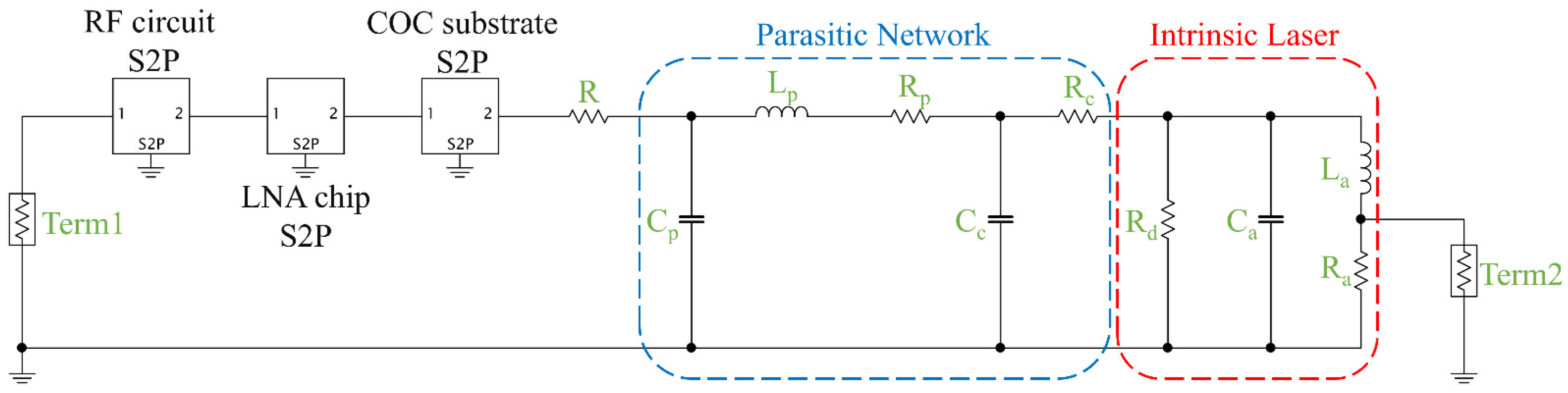
3.2. Co-Simulation of Optoelectronic Chips

To evaluate the effect of LNA on the gain of the module, we modelled the RF signal transmission equivalent circuit of the optical emission module. As shown in Figure 5, the intrinsic circuit of the laser is based on the rate equation. Ca and La represent the storage effects of carriers and photons in the active region, respectively. Ra and Rd are used to simulate the relaxation oscillation damping of the laser. The parasitic network mainly includes the chip parasitic network and the package parasitic network. The chip parasitic network is the contact capacitance and series resistance of the active region and the chip electrode, which are represented by Cc and Rc, respectively. The package parasitic network is the parasitic capacitance, inductance, and resistance introduced by the carrier and the gold wire in the package, which are represented by Cp, Lp, and Rp, respectively. The equivalent circuit also includes a series matching resistor R and S2P models of the COC substrate, LNA chip, and RF circuit.
Firstly, the equivalent circuit model containing only the laser intrinsic circuit, parasitic network, and the series matching resistor R was simulated. To extract the parameter values in the model, the transmission curve of the DML was measured using a vector network analyzer (VNA), and the model was fitted, as shown in Figure 6a. The S21 curve represents the transmission loss, and the S11 curve represents the return loss. The measurement results of S21 and S11 are consistent with the simulation results, which initially ensures the accuracy of the laser model. The specific component parameters are shown in Table 1. Finally, the complete equivalent circuit model of optical emission module was simulated, as shown in Figure 6b. In the range of 0.8~25 GHz, the gain is approximately 15 dB. Based on the above analysis, results show that the integration of the LNA chip and the DML chip in the optical emission module can effectively improve the signal gain.

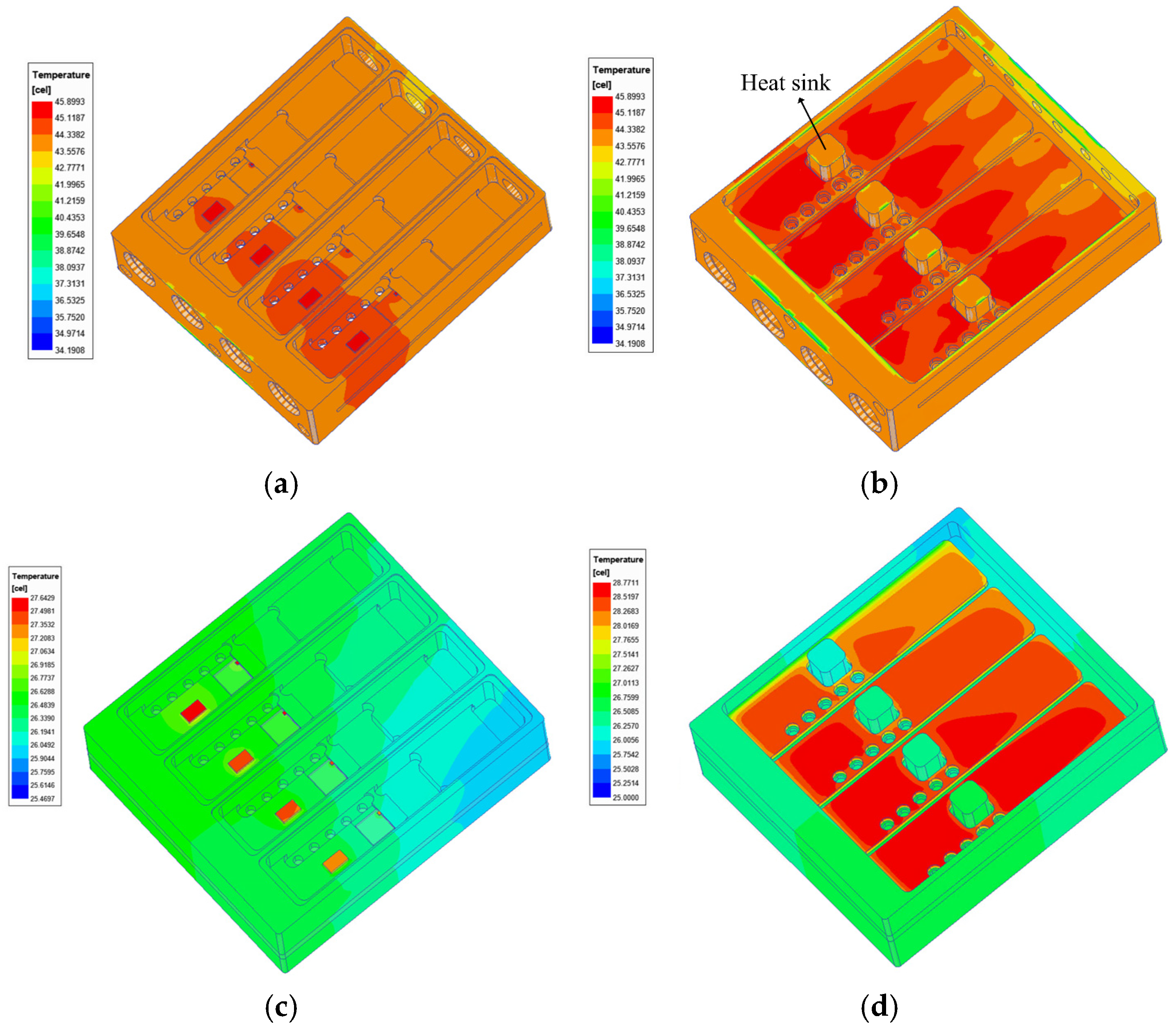
3.3. Thermal Simulation Design

Temperature significantly affects the performance and lifespan of laser modules. To enhance their heat dissipation capability in compact structures and thereby improve reliability, thermal design optimization is required. The following study simulates two cooling configurations: heat sink and microchannel structures. The primary heat transfer mode in the heat sink cooling solution is thermal conduction. Since copper is an excellent thermal conductor with a thermal conductivity of 400 W/(m·K) and a thermal expansion coefficient (CTE) of 1.77 × 10⁻⁵/°C, a copper heat sink is designed on the backside of the package structure. To further improve the heat dissipation capability of the module, a microchannel cooling structure is designed, as shown in Figure 7. The microchannel structure has a channel depth of 0.8 mm and a width of 0.6 mm. The complete cooling system comprises an optical emission module, a heat exchanger, a high-capacity reservoir, and a infusion pump. The detailed implementation measures are as follows: The coolant is pumped into the module interior to exchange heat with the components and then flows through an external heat exchanger where its temperature is regulated to 25 °C before circulating back to the reservoir tank. This ensures that the coolant entering the module each time remains at a constant 25 °C, ultimately forming a closed heat dissipation circulation loop.
Figure 8 shows the simulation results of the heat sink and microchannel cooling schemes at an ambient temperature of 25 °C. The results indicate that the temperatures of the module in the heat sink scheme are controlled below 50 °C, while the module using the microchannel scheme is maintained under 30 °C, demonstrating that the optimized thermal design effectively enhances the module’s heat dissipation capability.
Based on the microchannel liquid cooling solution, the module’s thermal performance was simulated across a wide temperature range of −55 °C to 75 °C. Multiple monitoring points were selected on the module during simulation, with the coolant temperature additionally maintained at 25 °C. As shown in Figure 9, the module consistently maintains its temperature below 30 °C, demonstrating the cooling structure’s high efficiency and its ability to enhance module reliability.

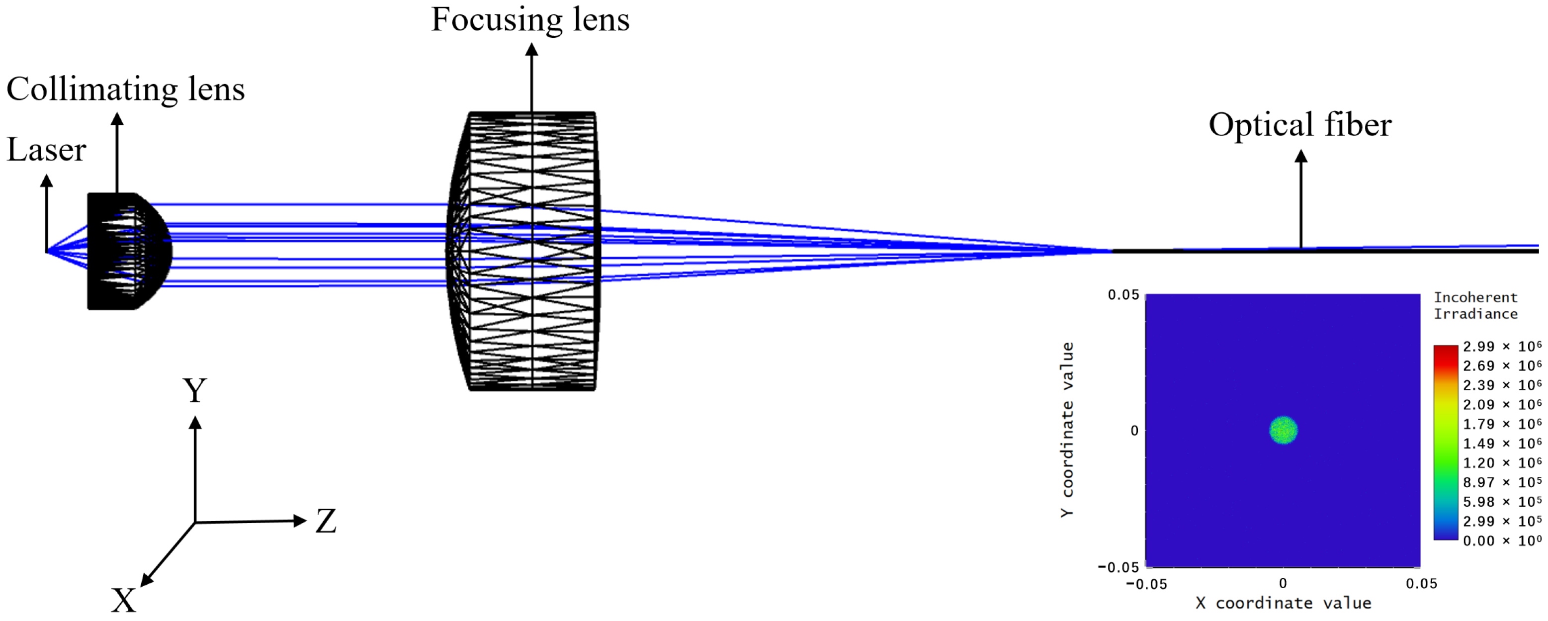
3.4. Optical Simulation Design

In the coupling method of double lenses and isolators, the collimating lens and focusing lens match the numerical aperture of the laser output and the optical fiber to improve the coupling efficiency. The isolator reduces light reflection from the component end face, preventing nonlinear effects caused by feedback into the laser. This ensures the modulation and spectral characteristics of the laser. As shown in Figure 10, the simulated coupling efficiency exceeds 70%, which represents an increase of 55 percentage points compared to the 15% efficiency achieved by direct coupling. This enhancement significantly improves both the coupling process tolerance and module reliability.
To provide a theoretical basis for practical coupling processes, simulations were conducted to determine the 3 dB tolerance ranges in the X, Y, and Z directions during coupling. These ranges correspond to the allowable displacement limits of the light source before the coupled power drops by 3 dB, as shown in Figure 11. The results indicate that the tolerance ranges are approximately ±0.8 μm in the X and Y directions and ±4 μm in the Z direction.

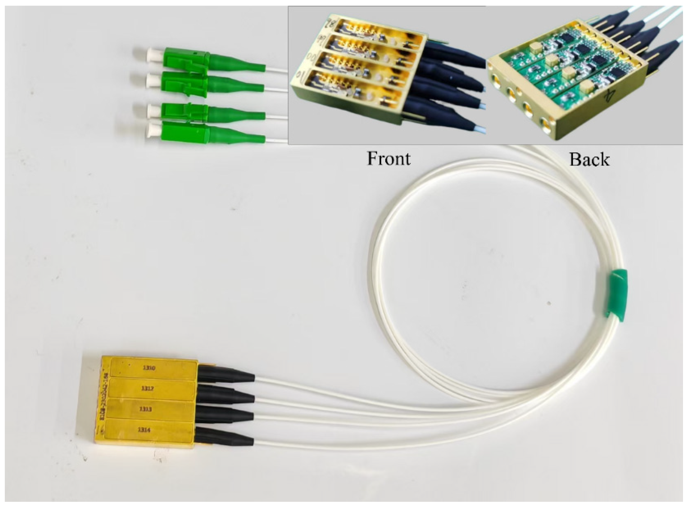
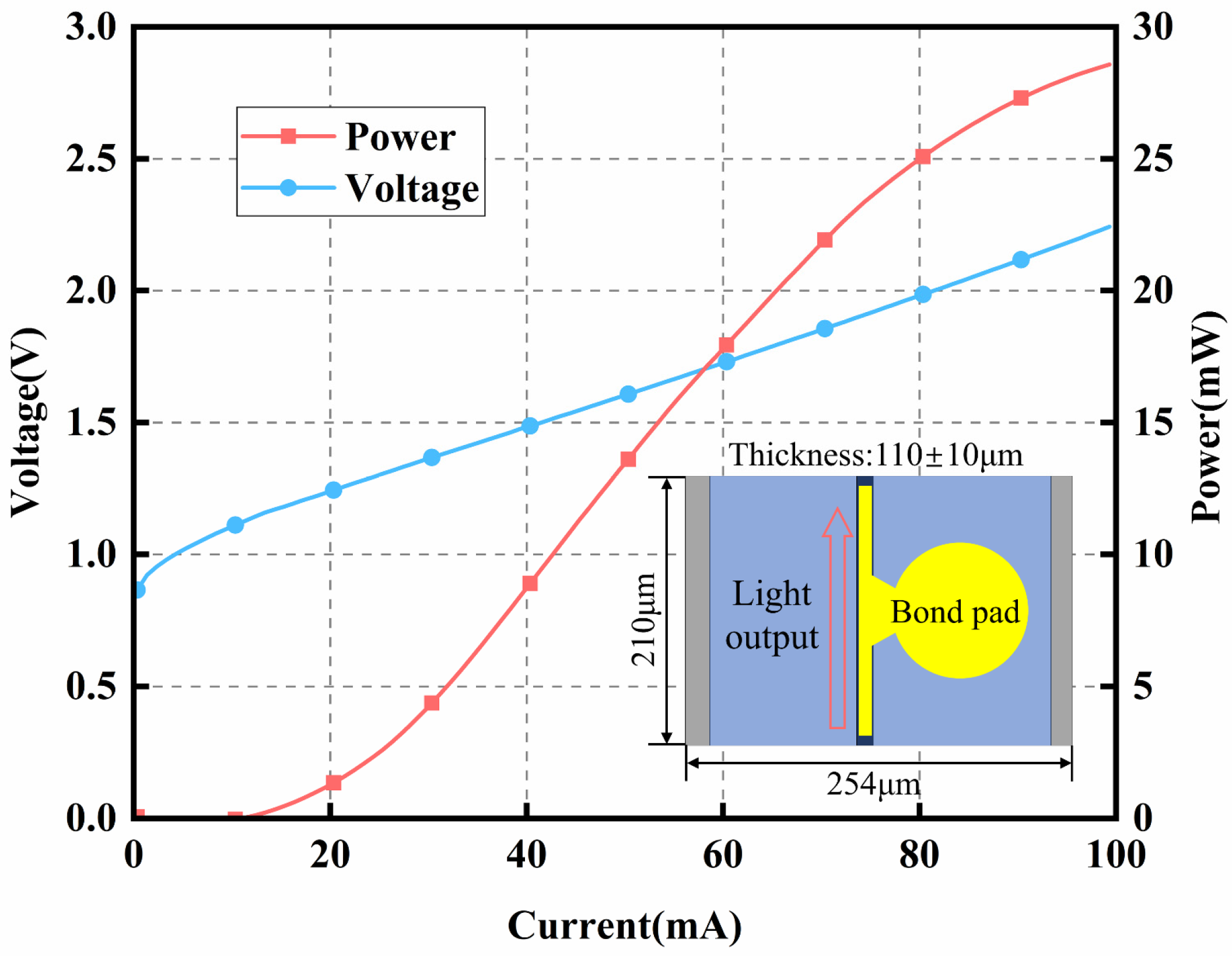
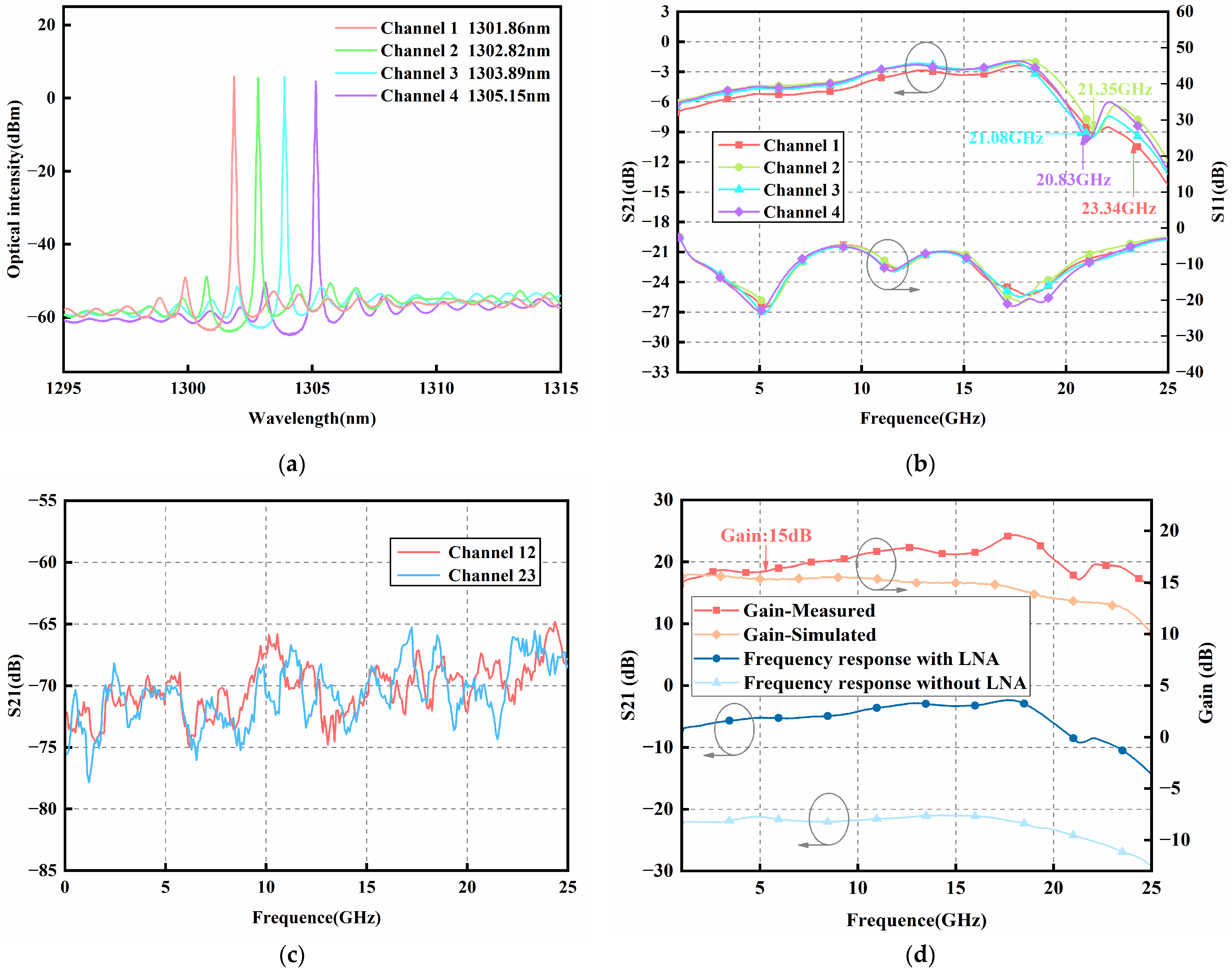
4. Experimental Results and Discussion

The photograph of the four-channel high-gain integrated optical emission module is shown in Figure 12. In the co-packaging process, the DML chip is first mounted to the COC substrate to make the COC component. Then, the TEC and control circuit are mounted inside the tube shell, and the COC component, the RF circuit, and LNA chip are mounted. After the assembly is completed, the RF and electrical connections are established using gold wire bonding. Finally, active coupling is used to couple the light from the DML chip into the optical fiber.
The DML chip is a commercial distributed-feedback (DFB) edge-emitting laser chip based on InP. The laser design adopts a ridge waveguide structure with a multi-quantum well (MQW) active layer and a DFB grating layer. The L-I-V curve and the schematic of the DML are shown in Figure 13. The DML in the module is biased at 60 mA, at which the output optical power is 17.5 mW. The maximum output optical power of the module is approximately 11.6 mW. As a result, the coupling efficiency of the method involving a double lens and an isolator can exceed 65%, which is in general agreement with the simulation results. Furthermore, the test results indicate that the tolerance ranges are approximately ±0.7 μm in the X and Y directions and ±3.8 μm in the Z direction, which is consistent with the simulation results.
The performance of the optical emission module was tested at an input voltage of ±5 V. The power consumption of a single channel of the module is 0.735 W. The power consumption of the DML, LNA, and TEC circuit is approximately 0.1 W, 0.35 W, and 0.28 W, respectively. As shown in Figure 14a, the module operates stably under the control of the circuit, with a channel wavelength spacing of approximately 1 nm. The wavelengths of the four channels in the optical emission module are 1301.86 nm, 1302.82 nm, 1303.89 nm, and 1305.15 nm, which belong to the 1310 nm band. The transmission loss and return loss of the four channels are shown in Figure 14b. The results show that the four channels have good consistency, and the −3 dB bandwidth of each channel exceeds 20 GHz, which is close to the simulation results. The RF signal crosstalk between neighboring channels is shown in Figure 14c. In the range of 0.8~25 GHz, the crosstalk is less than −65 dB. It indicates that the four chambers of the module can effectively suppress the RF signal crosstalk in the compact structure. In addition, the signal gain is tested and compared with the simulation results, as shown in Figure 14d. The test results show that the signal gain in the optical emission module with integrated LNA chip is approximately 15 dB in the range of 0.8~25 GHz, which is in line with the simulation results and meets the requirement of amplification. The observed discrepancy between simulated and measured gain characteristics may originate from parasitic parameters and impedance mismatch introduced by the actual packaging process.
The thermal stability of the module was experimentally validated over the specified ambient temperature range. As shown in Figure 15a, the power exhibits minimal variation with a deviation of approximately ±5% across the temperature range from −55 °C to 75 °C. The module’s bandwidth was tested at ambient temperatures of −55 °C, −15 °C, 35 °C, and 75 °C. Taking Channel 1 as an example, the results in Figure 15b demonstrate that the bandwidth exhibits minimal variation. In summary, the module demonstrates stable operation across the −55 °C to 75 °C temperature range, showing general agreement with simulation results. Although manufacturing tolerances and other non-ideal factors cause some performance degradation in experimental measurements, the module still meets application requirements.
By cascading the optical emission module with the photodetector, a directly modulated transmission link can be constructed, where the noise figure serves as a critical performance parameter of the optical link. The NF of the link was tested using a Ceyear 3986F noise figure analyzer over multiple frequencies, with the experimental setup shown in Figure 16.
To minimize noise figure measurement errors, the instrument should be calibrated prior to testing. The noise source is directly connected to the input port of the noise figure analyzer, and the start/stop frequencies along with the number of frequency points are set. After calibration, the noise figure at all frequency points approaches 0 dB. As shown in Table 2, the results indicate that the NF increases with the RF signal frequency while remaining below 30 dB. Compared to conventional optical emission modules, this module demonstrates significantly lower noise figures across the operational bandwidth [24].
Compared to traditional optical emission modules in prior research [15], this module innovatively integrates DMLs with LNA chips in a compact space to achieve 15 dB RF signal output gain. Additionally, it incorporates thermal management components including the TEC and control circuits to ensure highly reliable operation. Through the packaging design, the module achieves −65 dB crosstalk between neighboring channels. These advancements enable its applicability in high-performance and highly reliable optical communication systems.

5. Conclusions

In conclusion, a four-channel high-gain optical emission module is developed in this paper. The module integrates DML chips, LNA chips, and control circuits in the compact structure, with dimensions of only 24.4 mm × 21 mm × 5.9 mm. An equivalent circuit model of RF signal transmission is established to evaluate the approach of improving signal gain. The results between the model simulation and the experimental measurement are in good agreement. With optimized thermal management, the module can operate reliably in extreme ambient conditions (−55 °C to 75 °C). The module operates stably under the control of the circuit, with a channel wavelength spacing of approximately 1 nm, and the −3 dB bandwidth of each channel exceeds 20 GHz. The crosstalk between neighboring channels is less than −65 dB in the compact structure. In the range of 0.8~25 GHz, the four-channel gain is approximately 15 dB. The module maintains a noise figure below 30 dB. Through the co-packaging of the optical and electrical chips, the module can increase the module gain while enhancing integration. This work highlights the potential for applying this approach in optical phased array and other communication systems.

Author Contributions

Investigation, X.D. and M.C.; Methodology, Z.Z. (Zeping Zhao); Resources, Z.Z. (Zhike Zhang); Validation, X.D. and L.L.; Visualization, Z.Z. (Zeping Zhao); Writing—original draft, X.D. and L.L.; Writing—review and editing, X.D., Z.H., and T.Y. All authors have read and agreed to the published version of the manuscript.

Funding

This work was funded by the National Key Research and Development Program of China (2022YFB2803201).

Institutional Review Board Statement

Not applicable.

Informed Consent Statement

Not applicable.

Data Availability Statement

Data underlying the results presented in this paper are not publicly available at this time but may be obtained from the authors upon reasonable request.

Acknowledgments

We thank the Intelligent photon research group of the Institute of Semiconductors of the Chinese Academy of Sciences for the support for this work.

Conflicts of Interest

The authors declare no conflicts of interest.

References

  1. Zhu, Y.; Zou, K.; Ruan, X.; Zhang, F. Single Carrier 400G Transmission with Single-Ended Heterodyne Detection. IEEE Photonics Technol. Lett. 2017, 29, 1788–1791. [Google Scholar] [CrossRef]
  2. Kang, S.-K.; Huh, J.Y.; Lee, J.H.; Lee, J.K. Low-cost and miniaturized 100-Gb/s (2 × 50 Gb/s) PAM-4 TO-packaged ROSA for data center networks. Opt. Express 2018, 26, 6172–6181. [Google Scholar] [CrossRef]
  3. Rajpal, S.; Goyal, R. A Review on Radio-Over-Fiber Technology-Based Integrated (Optical/Wireless) Networks. J. Opt. Commun. 2017, 38, 19–25. [Google Scholar] [CrossRef]
  4. He, J.; Lee, J.; Kandeepan, S.; Wang, K. Machine Learning Techniques in Radio-over-Fiber Systems and Networks. Photonics 2020, 7, 105. [Google Scholar] [CrossRef]
  5. Chen, N.; Okada, M. Toward 6G Internet of Things and the Convergence with RoF System. IEEE Internet Things J. 2021, 8, 8719–8733. [Google Scholar] [CrossRef]
  6. Farsaei, A.; Wang, Y.; Molavi, R.; Jayatilleka, H.; Caverley, M.; Beikahmadi, M.; Shirazi, A.H.M.; Jaeger, N.; Chrostowski, L.; Mirabbasi, S. A review of wireless-photonic systems: Design methodologies and topologies, constraints, challenges, and innovations in electronics and photonics. Opt. Commun. 2016, 373, 16–34. [Google Scholar] [CrossRef]
  7. Zhao, Y.; Chen, L.; Aroca, R.A.; Zhu, N.; Ton, D.; Inglis, D.; Doerr, C.R. Silicon Photonic Based Stacked Die Assembly Toward 4×200-Gbit/s Short-Reach Transmission. J. Light. Technol. 2022, 40, 1369–1374. [Google Scholar] [CrossRef]
  8. Hong, Y.; Li, K.; Lacava, C.; Liu, S.; Thomson, D.J.; Meng, F.; Ruan, X.; Zhang, F.; Reed, G.T.; Petropoulos, P. High-Speed DD Transmission Using a Silicon Receiver Co-Integrated With a 28-nm CMOS Gain-Tunable Fully-Differential TIA. J. Light. Technol. 2021, 39, 1138–1147. [Google Scholar] [CrossRef]
  9. Li, W.; Zhang, H.; Hu, X.; Lu, D.; Chen, D.; Chen, S.; He, J.; Wang, L.; Qi, N.; Xiao, X.; et al. 100 Gbit/s co-designed optical receiver with hybrid integration. Opt. Express 2021, 29, 14304–14313. [Google Scholar] [CrossRef] [PubMed]
  10. Kanazawa, S.; Fujisawa, T.; Nunoya, N.; Ohki, A.; Takahata, K.; Sanjoh, H.; Iga, R.; Ishii, H. Ultra-Compact 100 GbE Transmitter Optical Sub-Assembly for 40-km SMF Transmission. J. Light. Technol. 2013, 31, 602–608. [Google Scholar] [CrossRef]
  11. Bhargava, P.; Kim, T.; Poulton, C.V.; Notaros, J.; Yaacobi, A.; Timurdogan, E.; Baiocco, C.; Fahrenkopf, N.; Kruger, S.; Ngai, T.; et al. Fully Integrated Coherent LiDAR in 3D-Integrated Silicon Photonics/65nm CMOS. In Symposium on VLSI Circuits; IEEE: Piscataway, NJ, USA, 2019; pp. C262–C263. [Google Scholar] [CrossRef]
  12. Kim, D.-W.; Au, K.Y.; Luo, X.; Ye, Y.L.; Bhattacharya, S.; Lo, G.Q. 2.5D Silicon optical interposer for 400 Gbps electronic-photonic integrated circuit platform packaging. In Proceedings of the IEEE 19th Electronics Packaging Technology Conference (EPTC), Singapore, 6–9 December 2017; pp. 1–4. [Google Scholar] [CrossRef]
  13. Aoki, T.; Sekiguchi, S.; Simoyama, T.; Tanaka, S.; Nishizawa, M.; Hatori, N.; Sobu, Y.; Sugama, A.; Akiyama, T.; Hayakawa, A.; et al. Low-Crosstalk Simultaneous 16-Channel × 25 Gb/s Operation of High-Density Silicon Photonics Optical Transceiver. J. Light. Technol. 2018, 36, 1262–1267. [Google Scholar] [CrossRef]
  14. Zhang, Z.; Liu, Y.; Wang, J.; Bai, J.; Yuan, H.; Wang, X.; Liu, J.; Zhu, N. Three-Dimensional Package Design for Electro-Absorption Modulation Laser Array. IEEE Photonics J. 2016, 8, 2700912. [Google Scholar] [CrossRef]
  15. Zhang, Z.Z.Z.; Liu, Y.L.Y.; An, J.A.J.; Zhang, Y.Z.Y.; Zhao, Z.Z.Z.; Liu, J.L.J.; Zhu, N.Z.N. 112 Gbit/s transmitter optical subassembly based on hybrid integrated directly modulated lasers. Chin. Opt. Lett. 2018, 16, 062501. [Google Scholar] [CrossRef]
  16. Zhao, Z.; Wang, J.; Han, X.; Zhang, Z.; Liu, J. Ultra-compact four-lane hybrid-integrated ROSA based on three-dimensional microwave circuit design. Chin. Opt. Lett. 2019, 17, 030401. [Google Scholar] [CrossRef]
  17. Yun, S.-J.; Han, Y.-T.; Kim, S.-T.; Shin, J.-U.; Park, S.-H.; Lee, D.-H.; Lee, S.-Y.; Baek, Y. Compact Hybrid-Integrated 4 × 80-Gbps TROSA Module Using Optical Butt-Coupling of DML/SI-PD and Silica AWG Chips. J. Light. Technol. 2021, 39, 2468–2475. [Google Scholar] [CrossRef]
  18. Jin, Y.; Xie, Y.; Zhang, Z.; Lu, D.; Yang, M.; Li, A.; Meng, X.; Qu, Y.; Li, L.; Shi, N.; et al. 4 × 112 Gb/s hybrid integrated silicon receiver based on photonic-electronic co-design. Chin. Opt. Lett. 2024, 22, 082501. [Google Scholar] [CrossRef]
  19. Benzoni, A.; Downie, M.; Kasper, B.; Paslaski, J.; Peral, E.; Wu, X.M.; Schrans, T.; Swass, M.; Tsai, C.; Ury, I. High speed, high performance laser module. In Proceedings of the 50th Electronic Components and Technology Conference (ECTC), Las Vegas, NV, USA, 21–24 May 2000; pp. 465–468. [Google Scholar] [CrossRef]
  20. Connelly, M.J. Semiconductor Optical Amplifiers; Kluwer Academic: Dordrecht, The Netherlands, 2002. [Google Scholar]
  21. Agrawal, G.P. Fiber-Optic Communication Systems; Wiley: Hoboken, NJ, USA, 2010. [Google Scholar]
  22. Pozar, D.M. Microwave Engineering; Wiley: Hoboken, NJ, USA, 2011. [Google Scholar]
  23. Han, W.; Rensing, M.; Wang, X.; Yang, H.; Peters, F.H.; O’Brien, P. Investigation of the Packaging-Induced RF Attenuations and Resonances in a Broadband Optoelectronic Modulator Module. J. Light. Technol. 2012, 30, 2610–2617. [Google Scholar] [CrossRef]
  24. Cox, C. High-performance fiber-optic links for microwave applications. In Proceedings of the IEEE MTT-S International Microwave Symposium Digest, Atlanta, GA, USA, 14–18 June 1993; pp. 719–722. [Google Scholar] [CrossRef]
Figure 1. (a) Block diagram, (b) the single chamber conceptual design, and (c) front configuration and (d) back configuration of the four-channel optical emission module.
Photonics 12 00425 g001
Figure 2. RF circuit and COC substrate model.
Photonics 12 00425 g002
Figure 3. Effect of signal line width W on the transmission performance.
Photonics 12 00425 g003
Figure 4. Effect of (a) the vias and (b) the distance D between the vias on the transmission performance.
Photonics 12 00425 g004
Figure 5. Equivalent circuit model of the optical emission module.
Photonics 12 00425 g005
Figure 6. (a) Measured and simulated results of the DML and (b) simulation results of the equivalent circuit model.
Photonics 12 00425 g006
Figure 7. The microchannel cooling structure.
Photonics 12 00425 g007
Figure 8. Thermal distributions at 25 °C. Heat sink scheme: (a) front side and (b) back side. Microchannel scheme: (c) front side and (d) back side.
Photonics 12 00425 g008
Figure 9. Temperature in the microchannel scheme across a range of −55 °C to 75 °C.
Photonics 12 00425 g009
Figure 10. Simulated coupling efficiency of the coupling scheme.
Photonics 12 00425 g010
Figure 11. The 3 dB tolerance ranges in the X, Y, and Z directions.
Photonics 12 00425 g011
Figure 12. Photograph of the four-channel high-gain integrated optical emission module.
Photonics 12 00425 g012
Figure 13. The L-I-V curve and the schematic of the DML.
Photonics 12 00425 g013
Figure 14. (a) Wavelengths of four channels, (b) transmission loss and return loss, (c) RF signal crosstalk between neighboring channels, and (d) test results of S21 and the measured and simulated gains.
Photonics 12 00425 g014
Figure 15. (a) Power and (b) bandwidth of the module at different temperatures.
Photonics 12 00425 g015
Figure 16. Experimental setup for NF measurement.
Photonics 12 00425 g016
Table 1. Equivalent circuit model parameters of the optical emission module.
CaLaRaRdCcRcCpLpRpR
76.80.816.690.183.394.8398.20.220.9740
pFpHpFΩfFnHΩΩ
Table 2. The noise figure of the module.
Frequency (GHz)Noise Figure (dB)Frequency (GHz)Noise Figure (dB)
422.821225.58
623.341426.02
824.371627.18
1025.251829.49
Disclaimer/Publisher’s Note: The statements, opinions and data contained in all publications are solely those of the individual author(s) and contributor(s) and not of MDPI and/or the editor(s). MDPI and/or the editor(s) disclaim responsibility for any injury to people or property resulting from any ideas, methods, instructions or products referred to in the content.

