Article

High-Speed 2x1 Multiplexer with Carrier-Reservoir Semiconductor Optical Amplifiers

by
Amer Kotb
1,2,*,
Kyriakos E. Zoiros
3 and
Wei Chen
1,*
1
School of Chips, XJTLU Entrepreneur College (Taicang), Xi’an Jiaotong-Liverpool University, Taicang, Suzhou 215400, China
2
Department of Physics, Faculty of Science, University of Fayoum, Fayoum 63514, Egypt
3
Lightwave Communications Research Group, Department of Electrical and Computer Engineering, School of Engineering, Democritus University of Thrace, 67100 Xanthi, Greece
*
Authors to whom correspondence should be addressed.
Photonics 2024, 11(7), 648; https://doi.org/10.3390/photonics11070648
Submission received: 13 June 2024 / Revised: 5 July 2024 / Accepted: 8 July 2024 / Published: 10 July 2024
(This article belongs to the Special Issue Novel Advances in Optical Communications)

Abstract

:
Leveraging the rapid carrier recovery times and minimal polarization sensitivity of carrier-reservoir semiconductor optical amplifiers (CR-SOAs), this study embeds them in a Mach–Zehnder interferometer (MZI) setup to emulate a 2x1 multiplexer (MUX) operating at 120 Gb/s. The focus is on incorporating AND logic gate functionalities into the CR-SOAs-based MZI structure to facilitate high-quality multiplexing. The proposed methodology utilizes the intrinsic gain and phase modulation capabilities of CR-SOAs-based MZI to effectively manipulate data streams. This innovative approach capitalizes on the unique properties of CR-SOAs, such as fast response times and low polarization sensitivity, to achieve optimal signal transmission quality and efficient multiplexing. To assess MUX performance, a quality factor metric is introduced as a comprehensive measure of signal integrity. Through exhaustive simulations and meticulous analysis, the study demonstrates the feasibility of achieving the desired data rate while maintaining superior signal transmission quality. The results underscore the efficacy of CR-SOAs-based MZI as versatile modules for high-speed multiplexing applications, offering unparalleled performance and efficiency. This research represents a significant advancement in understanding optical communication systems and provides valuable insights for optimizing signal quality and mitigating interference in practical real-world scenarios.

1. Introduction

In response to escalating demands for increased data throughput in optical communication systems, the development of efficient multiplexing techniques has become imperative. Multiplexers (MUXs) play a pivotal role by consolidating multiple data streams into a single channel, thereby optimizing bandwidth utilization and enabling seamless data transmission. Previous research has extensively explored methodologies for designing all-optical logic MUXs, utilizing technologies such as photonic crystals (PhCs) and conventional semiconductor optical amplifiers (SOAs) [1,2,3,4,5,6,7]. However, the sluggish dynamic response of conventional SOAs often hampers their efficiency, particularly at speeds exceeding 100 Gb/s in modern optical communication systems [1]. Within the spectrum of all-optical multiplexing techniques, Mach–Zehnder interferometers (MZIs) have emerged as versatile and scalable solutions [8,9]. Integration of carrier-reservoir semiconductor optical amplifiers (CR-SOAs) into MZI configurations presents a promising avenue for achieving high-speed multiplexing functionalities. CR-SOAs are distinguished by their rapid carrier recovery and minimal polarization sensitivity, making them ideally suited for high-speed optical signal processing applications [10,11,12,13,14,15,16]. Recent studies have explored novel applications of CR-SOA-based MZIs, including the emulation of complex logic functions [10,11,12,13,14,15,16]. This study focuses on leveraging CR-SOA-based MZIs to simulate a 2x1 MUX configured as AND logic gates to enhance data manipulation efficiency and multiplexing capabilities at ultra-high data rates. Performance evaluation criteria include signal integrity metrics, particularly the quality factor (QF), for comprehensive assessment. To expand the state of the art, relevant studies were selected based on their contributions to CR-SOA-based MZIs, MUX design, and high-speed data processing. Inclusion criteria emphasized papers showcasing innovative applications of CR-SOAs in optical logic gates and MUX configurations, while exclusion criteria ensured studies unrelated to high-speed optical signal processing or lacking comprehensive QF analysis were excluded. By investigating the utilization of CR-SOA-based MZIs as AND logic gates for simulating a 2x1 MUX operating at 120 Gb/s, this research aims to demonstrate the feasibility and effectiveness of the proposed scheme in achieving high-speed data multiplexing while maintaining optimal signal transmission quality. Through meticulous simulations and analysis, we contribute to advancing CR-SOA-based MZIs as versatile components in high-speed optical communication systems, thereby enhancing multiplexing efficiency and optimizing signal integrity for practical applications.
The remainder of this paper is structured as follows: Section 2 elaborates on the principle of operation of CR-SOAs in Section 2.1, followed by explanations of the AND logic gate in Section 2.2 and the 2x1 MUX configuration in Section 2.3. Section 3 outlines the simulation methodology employed to evaluate the performance of CR-SOA-based MZIs as AND logic gates for the 2x1 MUX operating at 120 Gb/s. Section 4 presents and discusses the simulation results, focusing on the QF against the key operational parameters. In Section 5, a comparative analysis is conducted to highlight the advantages of the proposed CR-SOA-based MZI approach over existing designs. Section 6 discusses experimental and scalability challenges. Section 7 concludes the paper by summarizing key findings.

2. Principle of Operation

2.1. CR-SOA

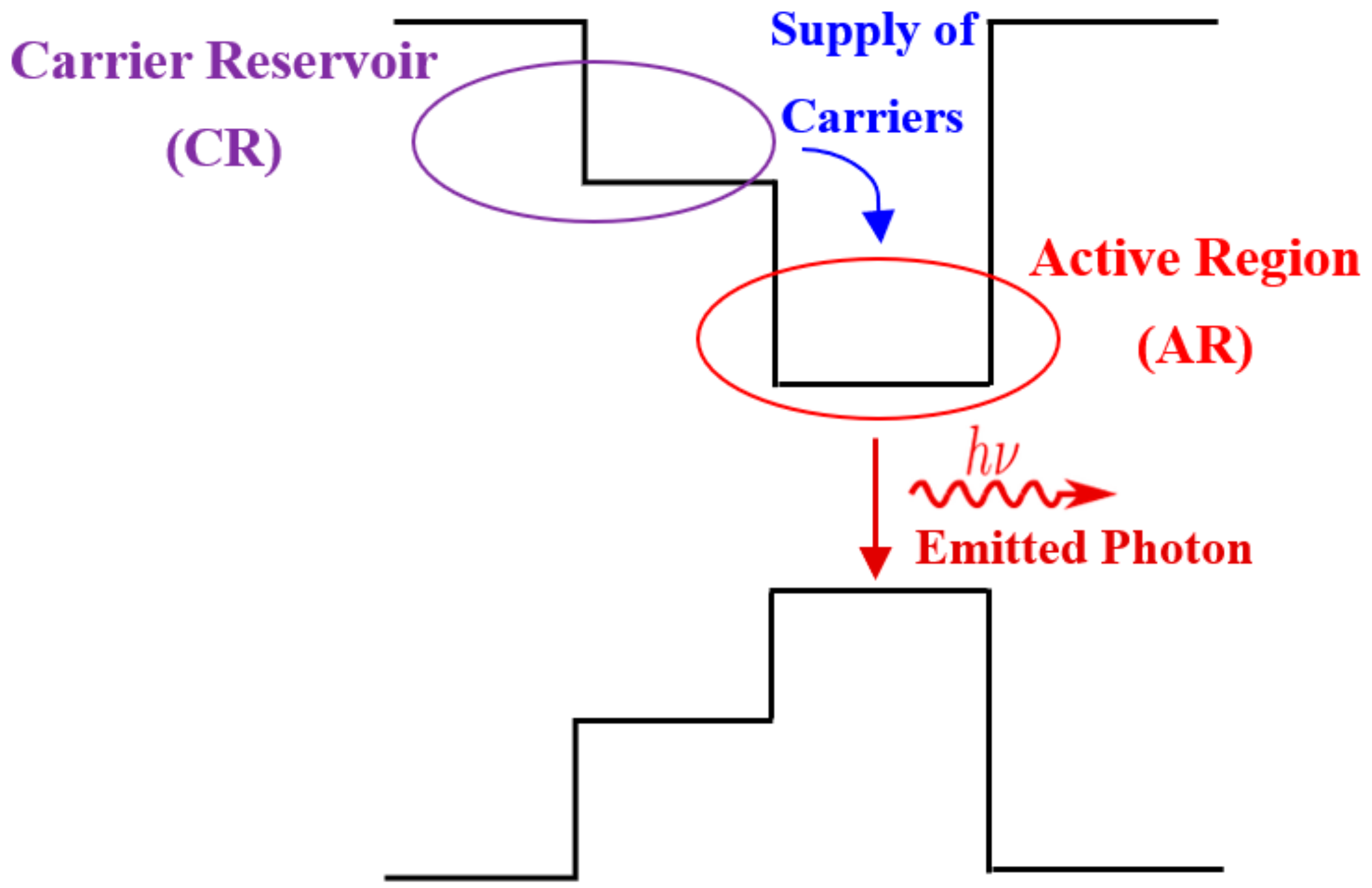
Illustrated in Figure 1 [10,12,15], the faster response of CR-SOA resembles that of quantum dot (QD) SOA [17,18], as both utilize a carrier reservoir concept. In CR-SOA, the CR region is situated near the active region. Under favorable conditions, the CR becomes highly populated, delivering carriers to the active region with a transition time comparable to QD-SOA, typically around 0.5–10 ps. This ultra-fast transition governs gain dynamics, leading to swift temporal gain and phase responses [16].

2.2. AND

In the operation of the AND gate with CR-SOAs-MZI, the system functions such that an output of ‘1’ is produced only when both inputs are ‘1’. Specifically, data A is employed as a pump beam and directed into the upper arm of the CR-SOAs-MZI (CR-SOA1) via a wave-selective coupler (WSC). Concurrently, signal B is split equally by a 3 dB optical coupler (OC) into two parts, which traverse through the middle arm of the CR-SOAs-MZI1 (CR-SOA1 and CR-SOA2). Additionally, a continuous-wave (CW) beam is introduced into the lower arm of the CR-SOAs-MZI (CR-SOA2), as shown in Figure 2. The phase modulation of signal B is controlled by data A through cross-phase modulation (XPM) in CR-SOAs. When A = ‘0’, no phase window is opened for both B = ‘0’ and B = ‘1’, resulting in an output of ‘0’ at the 3 dB OC output. If A = B = ‘1’, constructive interference occurs, yielding an output of ‘1’. Conversely, if A = ‘1’ and B = ‘0’, the output is ‘0’ due to the absence of an input signal to disrupt the initially balanced CR-SOAs-MZI. Thus, the output of the CR-SOAs-MZI represents ‘1’ only when both A and B are ‘1’, akin to the AND logic gate after the application of an optical bandpass filter (OBPF) to eliminate any undesirable wavelengths, as shown in the attached truth table.

2.3. 2x1 MUX

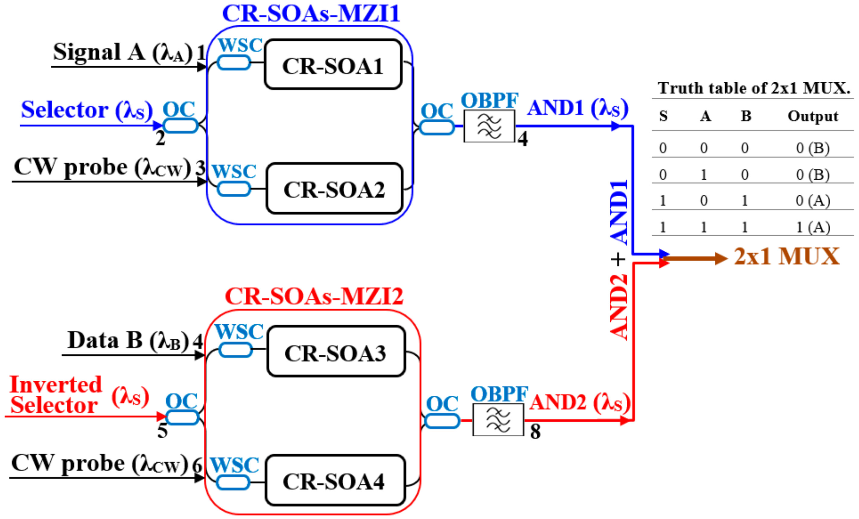
In the configuration utilizing MZI1 for AND1 and MZI2 for AND2 within the 2x1 MUX setup, each MZI acts as a logical AND gate, as shown in Figure 3. For AND1, signal A and a CW are directed into the two arms of CR-SOAs-MZI1. Simultaneously, the selector signal (S) is introduced into the middle arm. The selector signal’s presence or absence determines whether the signal from input A passes or not, respectively, through MZI1. When the selector signal is active (at logic level ‘1’), it modulates the signal’s path, allowing it to influence the output intensity. This configuration effectively implements the logical AND operation between the input signal A and the selector signal. For AND2, signal B and another CW are directed into the two arms of CR-SOAs-MZI2. In this case, the inverted selector signal ( S ¯ ) is introduced into the middle arm. Similar to CR-SOAs-MZI1, the inverted selector signal controls the switching of signal B based on its logic level. When the inverted selector signal is active (at logic level ‘0’), it modulates the path of signal B through CR-SOAs-MZI2. As a result, the output intensity corresponds to the logical AND operation between input signal B and the inverted selector signal. Then, the outputs AND1 and AND2 are combined at the output port to constitute the 2x1 MUX. The final output is logically expressed by Y = S . A + S ¯ . B . This indicates that both A and B must be equal to ‘1’ for the overall expression to be true. If either A or B (or both) is equal to ‘0’, the expression amounts to ‘0’. By combining the outputs of AND1 and AND2, the MUX provides for signal switching and logic functionalities, thereby facilitating robust and efficient optical signal processing tailored to the specific states of the selector signals. This approach enhances the versatility and effectiveness of the MUX setup, making it well-suited for a diverse range of applications in optical communication and signal processing systems.

3. Simulation

The complex behavior of carrier reservoirs in CR-SOAs is accurately described by a set of coupled differential equations. These equations represent the detailed interactions between carriers, photons, and other significant parameters. In particular, they incorporate the nonlinear intraband effects of spectral hole burning (SHB) and carrier heating (CH) as follows [15,16]:
d h A R ( t ) d t   =   h C R ( t ) - h A R ( t ) τ t ( 1 + η )   +   η h 0 τ c ( 1 + η )     h A R ( t ) τ c     ( e x p   [ h A R ( t )   +   h C H ( t )   +   h S H B ( t ) ]     1 )   P i n ( t ) E s a t
d h C R ( t ) d t   =   η ( h C R ( t ) - h A R ( t ) τ t ( 1 + η )   +   h 0 h C R ( t ) τ c ( 1 + η )     h C R ( t ) τ c
d h C H ( t ) d t   =   h C H ( t ) τ C H     ε C H τ C H ( e x p   [ h A R ( t )   +   h C H ( t )   +   h S H B ( t ) ]     1 )   P i n ( t )
d h S H B ( t ) d t   =     h S H B ( t ) τ S H B     ε S H B τ S H B ( e x p   [ h A R   ( t )   +   h C H ( t )   +   h S H B ( t ) ]     1 )   P i n ( t )     d h A R ( t ) d t     d h C H ( t ) d t
where the functions hAR, hCR, hCH, and hSHB describe the gain of the CR-SOA integrated across its length, incorporating carrier recombination between AR and CR, as well as the effects of CH and SHB. The population inversion factor, η, defined as NAR/NCR, indicates the ratio of carrier densities between the active region and the carrier reservoir, reflecting the state of population inversion in the CR-SOA. The unsaturated power gain of the CR-SOA is expressed as G0 = exp[h0] = αΓ(Iτc/eV − Ntr)L and its saturation energy is characterized by Esat = Psat τc = wdћω0/αΓ [10]. Detailed information on these parameters, including their values and definitions, is provided in Table 1 [1,2,3,4,5,6,7,8,9,10,11,12,13,14,15,16]. These parameters are derived from experimental studies typically involving semiconductor materials optimized for optical amplification and modulation characteristics. Semiconductor materials such as InGaAsP and InP are commonly utilized in (CR)-SOAs integrated within MZI configurations, aimed at achieving high gain, low noise, and fast response times suitable for high-speed data transmission. These materials play a critical role in validating theoretical predictions by ensuring robust signal integrity and efficient optical processing in advanced optical communication systems. For specific details on the semiconductor materials and experimental setups used in the studies referenced, consulting the original papers would provide comprehensive insights.
In optical communication and signal processing, Gaussian-shaped return-to-zero (RZ) pulses improve bandwidth efficiency and signal-to-noise ratios. Their controlled rise and fall times minimize distortions, enhancing transmission and detection [19,20]. For these reasons, the input optical power (Pin(t)) for signals A, B, and S is represented by Gaussian-shaped RZ pulses, as established in previous studies [10,12,15].
P i n ,     C R S O A ( t ) =   n   =   1 K a n ( A ,   B ,   S )     2 ln [ 2 ]       E 0 π       τ F W H M     e x p - 4 ln [ 2 ]     ( t     -     n   T ) 2 τ F W H M 2
where αn(A, B, S) denotes the nth pulse within the A, B, or S signals and K (=27 − 1) is the length of a pseudorandom binary sequence (PRBS).
The upper arm of CR-SOAs-MZI1 receives power PA(t) from signal A along with half of the power PS(t) from the selector signal. Simultaneously, the lower arm of CR-SOAs-MZI1 is supplied with power PCW from the CW beam. Thus, the configuration precisely defines the input optical powers for the AND1 function as follows [12]:
P i n ,     C R S O A 1 ( t )   =   P A ( t )   +   0.5   P S ( t )
P i n ,     C R   S O A 2 ( t )   =   P C W   +   0.5   P S ( t )
Within the CR-SOAs-MZI2 setup, power PB(t) is merged with half of the inverted select signal power P S ¯ ( t ) and directed into the upper arm. At the same time, power PCW is fed into the lower arm. This configuration defines the input optical powers for the AND2 function as follows [12]:
P i n ,     C R S O A 3 ( t )   =   P B ( t )   +   0.5   P S ¯ ( t )
P i n ,     C R S O A 4 ( t )   =   P C W   +   0.5 P S ¯ ( t )
The formula for calculating the gain for each CR-SOA is as follows [10,12,15]:
G C R S O A i ( t )   =   e x p   [ h A R ( t )   +   h C H ( t )   +   h S H B ( t )   ] ,             i =   1 , 2 , 3 , 4
The ensuing equations delineate the phase modulation experienced by the selector signals within each CR-SOA [10,12,15]:
Φ C R S O A i ( t )   =     0.5   α   h A R ( t )     +     α C H   h C H ( t ) ,               i = 1 , 2 , 3 , 4
It is worth mentioning that the contribution of SHB is assumed negligible, as indicated by the null linewidth enhancement factor, i.e., αSHB = 0 [10,12,15].
The output powers for AND1 and AND2 are derived using the interferometric formula indicated below [12]:
P A N D 1 ,   2 ( t ) =   0.25   P S ,     S ¯ ( t )   G C R S O A 1 ,   3 ( t )     +     G C R S O A 2 ,   4 ( t )         2 G C R S O A 1 ,   3 ( t )   G C R S O A 2 ,   4 ( t )     c o s   [ Φ C R S O A 1 ,   3 ( t )         Φ C R S O A 2 ,   4 ( t ) ]
The outputs of the AND1 and AND2 gates, computed from Equation (12), are combined to form the MUX gate. The output power of the MUX gate is consequently determined by their sum as follows [21]:
P o u t ,     M U X ( t )   =   P A N D 1 ( t )   +   P A N D 2 ( t )
In Wolfram Mathematica®, we utilized the Adams numerical technique to solve Equations (1)–(13). The QF in optical communication systems is a critical measure of signal integrity, defined by the expression QF = (P1 − P0)/(σ1 + σ0), where P1 and P0 are the mean power levels of the signal for bits ‘1’ and ‘0’, and σ1 and σ0 are their respective standard deviations (noise). A higher QF indicates better signal quality and a lower bit error rate (BER), which is the rate of errors in the transmission. The relationship between QF and BER is given by BER ≈ 0.5 erfc[QF/ 2 ], where erfc is the complementary error function. Achieving a QF of at least 6 is crucial to ensure a BER below 10−9, a standard benchmark for high-quality optical communication, thus highlighting the importance of QF in maintaining efficient and reliable data transmission [10,12,15].

4. Results and Discussion

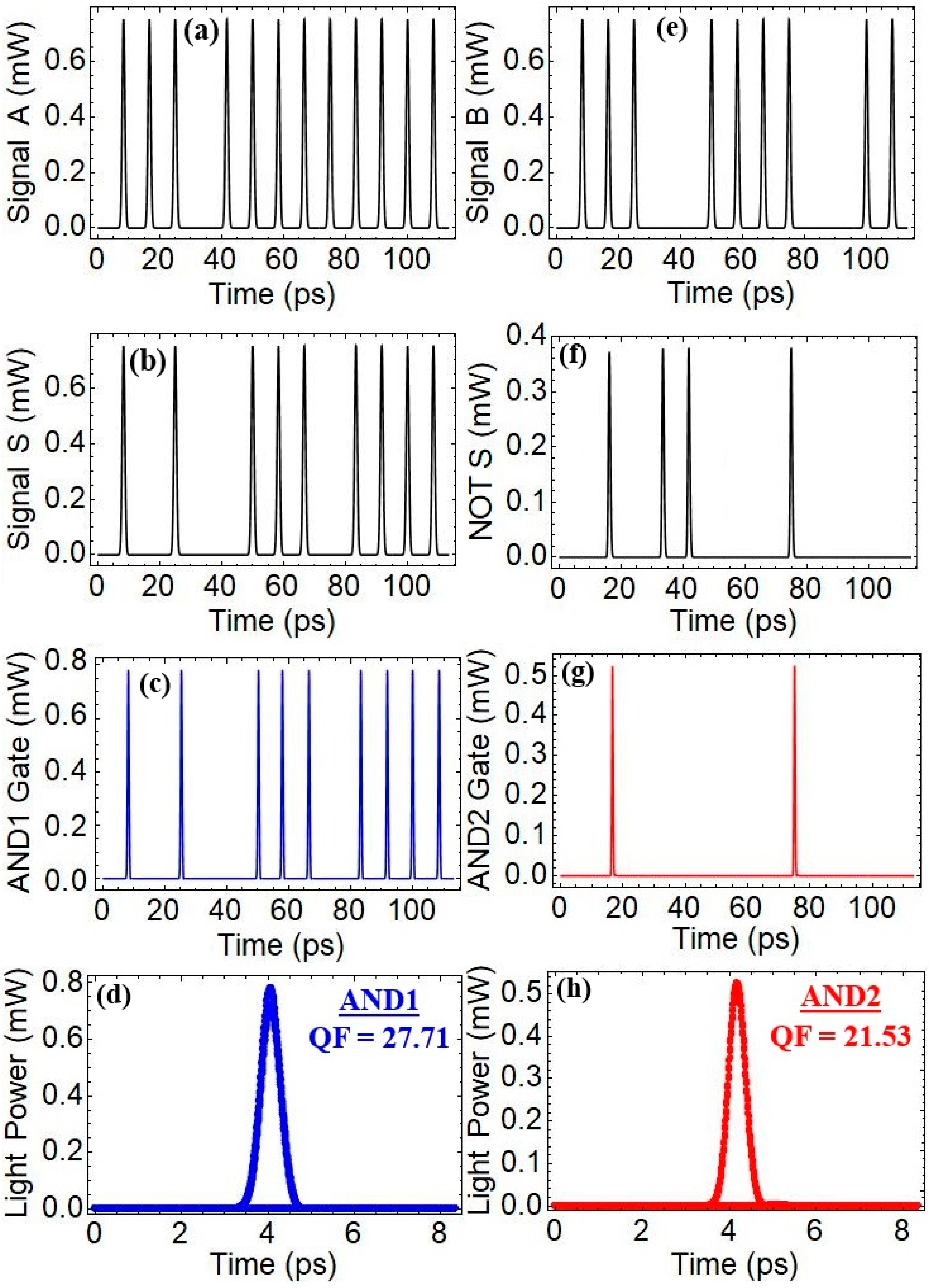
The proposed 2x1 MUX scheme using CR-SOAs-MZIs at 120 Gb/s enables obtaining the AND gate output’s enhanced QF values of 27.71 for AND1 and 21.53 for AND2, as shown in Figure 4. The differences in QFs between AND1 and AND2, both employing CR-SOAs within their respective MZI configurations, can be attributed to several factors. While both MZIs are designed to function as logical AND gates, variations in how the selector signals (S and S ¯ ) modulate the optical paths within MZI1 and MZI2 setups may lead to nuanced differences in performance metrics such as QF. These variations could stem from subtle differences in device characteristics, including gain and response time, or from operational conditions such as temperature fluctuations and input signal variations. Despite using the same type of CR-SOAs, these factors can influence the optical performance differently in each MZI configuration, potentially resulting in the observed differences in QF values between AND1 and AND2. However, both AND1 and AND2 are designed to effectively perform logical AND operations, contributing to the overall functionality and performance of the 2x1 MUX setup at 120 Gb/s. These values indicate that the CR-SOAs effectively maintain signal integrity, which is essential for high-speed data transmission. Overall, these results highlight the improved performance of the AND gates employing the proposed MUX scheme, underscoring its potential for reliable operation in advanced optical communication systems. Additionally, the 2x1 MUX using CR-SOAs-based MZIs at 120 Gb/s demonstrates significant performance, with a QF of 8.85, as depicted in Figure 5. This high QF indicates excellent signal integrity and minimum BER, which is essential for high-speed optical communication. The embedding of CR-SOAs in MZIs effectively enhances the amplification and switching capabilities, ensuring robust data transmission even at elevated data rates. The integration of CR-SOAs within MZI structures for multiplexing applications offers promising advancements in optical communication, providing reliable signal transmission and maintaining high data integrity at accelerated data rates.
In a 2x1 MUX using CR-SOAs and MZIs at 120 Gb/s, the QF is highly influenced by pulse energy (E0) and pulse width (τFWHM). Higher E0 generally enhances the QF; however, if E0 is too high, stronger carrier depletion is caused and hence the QF is reduced. Conversely, lower E0 reduces saturation and nonlinear effects, resulting in higher output signal QF and improved signal fidelity [12,22,23]. Regarding τFWHM, narrower pulses support higher data rates and better temporal resolution, which is essential for maintaining 120 Gb/s, but they are more susceptible to dispersion, leading to pulse broadening and inter-symbol interference that can reduce QF. Wider pulses are less affected by dispersion and maintain their shape over longer distances, thus preserving signal quality and improving QF, but they limit the maximum data rate by allowing fewer pulses per time unit [12,24,25]. Figure 6 depicts the QF against E0 and τFWHM for the AND1, AND2, and MUX utilizing CR-SOAs-MZIs at 120 Gb/s. Therefore, achieving a high QF in the 2x1 MUX using CR-SOAs-MZIs at 120 Gb/s requires optimizing both E0 and τFWHM to balance strong SNR, ensuring high signal QF.
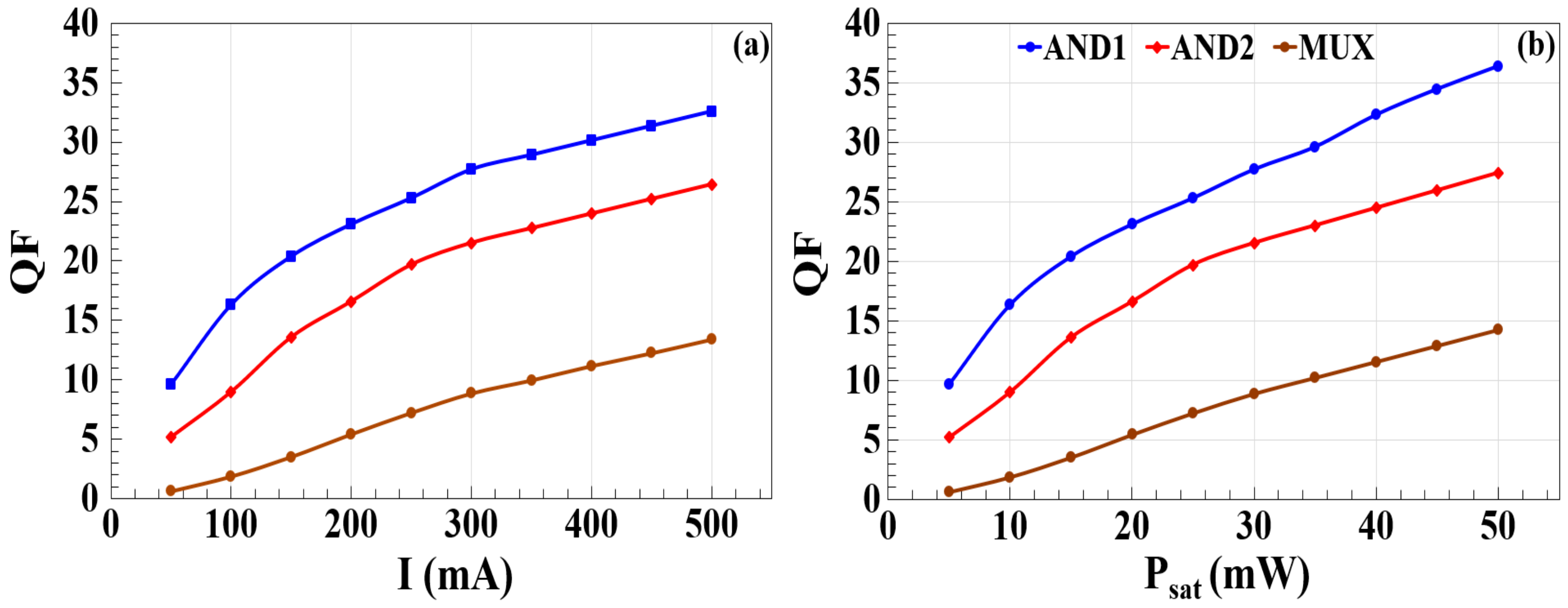
The study analyzed the QF against the injection current (I) and saturation power (Psat) for the AND1, AND2, and 2x1 MUX logic gates using CR-SOAs-MZIs at 120 Gb/s, as shown in Figure 7. For all three configurations (AND1, AND2, and MUX), increasing I initially improves the QF as the CR-SOAs provide higher gain and signal amplification. However, beyond an optimal I, further increases can lead to thermal effects and nonlinearities that degrade the QF [26]. On the other hand, Psat represents the input optical power level at which the gain of the amplifier reaches its maximum value and begins to saturate. As the input power increases beyond this saturation point, the gain decreases, leading to distortion and degradation in signal quality. Therefore, fine-tuning both I and Psat is essential for optimizing the performance and maintaining high signal integrity of MUX operation at high-speed data rates.
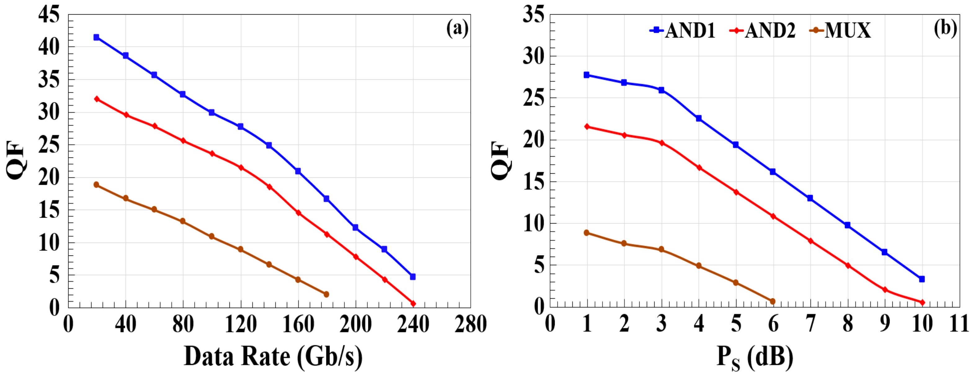
To gain deeper insights into the performance of the proposed scheme, Figure 8a illustrates the QF versus the operating data rate and the incident power of the selector signal for AND1, AND2, and the 2x1 MUX using CR-SOAs-MZIs. The CR-SOA is expected to function at higher speeds while maintaining satisfactory performance. The examined optical gates show acceptable QF values at elevated data rates, attributed to the rapid transitions facilitated by the CR layer. For instance, AND1 achieves a QF of 8.83 at 220 Gb/s, AND2 reaches a QF of 7.83 at 200 Gb/s, and the 2x1 MUX attains a QF of 6.56 at 140 Gb/s. These results demonstrate the capability of CR-SOAs-MZIs to support high-speed data transmission with reliable performance, highlighting their potential for use in advanced optical communication systems. The ability to maintain high QF values at increased data rates indicates that these devices can effectively handle the demands of next-generation high-speed networks, ensuring signal integrity and efficient data processing. Additionally, the performance of the 2x1 MUX using CR-SOAs is influenced by the power of the incident selector signal (PS). The QF varies with changes in PS, as this power level directly affects the switching dynamics and the efficiency of MUX. Higher PS can enhance the switching speed, leading to improved QF. However, excessively high power can introduce saturation in the CR-SOAs, which may degrade the QF, as shown in Figure 8b. Therefore, it is crucial to optimize the selector signal power to achieve the best balance between switching performance and signal integrity. This optimization ensures that the 2x1 MUX can efficiently manage data streams with high reliability and minimal error rates, further solidifying its suitability for high-speed optical communication networks.
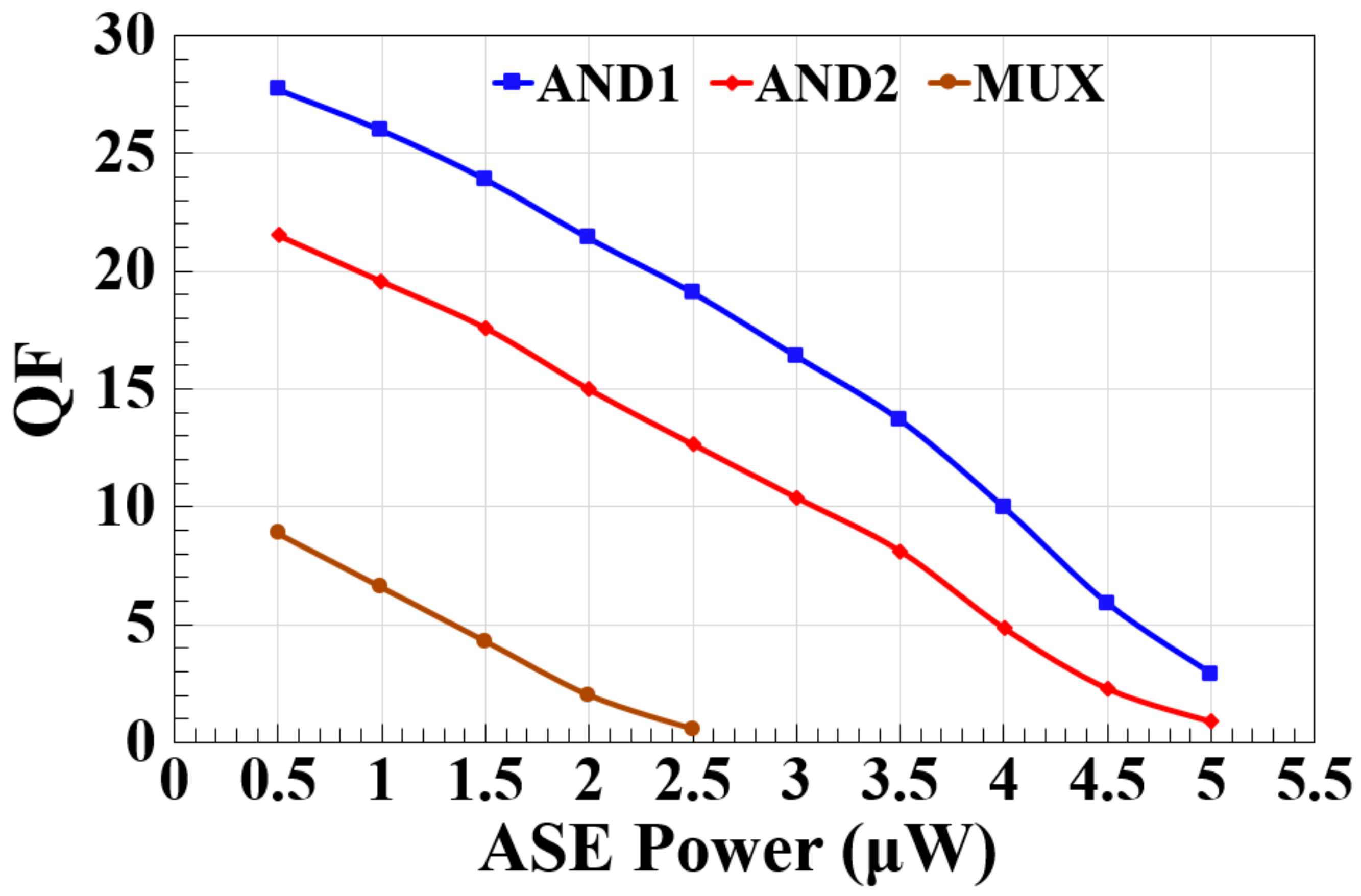
Studying the impact of ASE (amplified spontaneous emission) on CR-SOAs-based optical systems operating at 120 Gb/s is essential for comprehensively understanding and optimizing the performance of advanced high-speed optical communication technologies. ASE noise introduces significant additional noise into the optical signal path, thereby deteriorating the signal-to-noise ratio and potentially compromising the fidelity of data transmission. Our investigation focuses on analyzing the QF variation against ASE for individual components such as AND1, AND2, and the MUX implemented using CR-SOAs. ASE power PASE was meticulously calculated using PASE = NSP (G0 − 1) 2πℏνB0 [10,12,15]. Our findings demonstrate a pronounced decrease in QF with increasing ASE power levels, as shown in Figure 9. These results underscore the critical impact of ASE noise on signal integrity and emphasize the imperative of implementing effective strategies to mitigate ASE effects. Such strategies include optimizing device parameters, employing advanced noise-reduction techniques, and adjusting operational conditions to sustain optimal signal quality and reliability in next-generation optical communication networks. By refining our understanding through ASE studies, we not only enhance the design and deployment of CR-SOAs-based optical systems but also contribute significantly to advancing the efficiency and resilience of modern optical communication infrastructures.
To achieve maximum performance in CR-SOA-based MZIs within a 2x1 MUX setup, it is essential to balance several critical parameters, as illustrated in Figure 6, Figure 7, Figure 8 and Figure 9. Pulse energy and injection current play pivotal roles in enhancing signal intensity and speed, with optimal performance often requiring moderate levels to prevent excessive power consumption and mitigate ASE noise and saturation effects, which can degrade system reliability. Pulse width and selector signal power are equally crucial, affecting signal modulation efficiency and precise control over logical operations within the MZIs. Saturation power defines the maximum optical power before nonlinear effects compromise performance, necessitating careful management to maintain signal integrity. Additionally, data rate impacts processing speed and requires synchronized adjustments in energy levels and response times to ensure efficient data transmission. Minimizing ASE power is critical to preserving signal quality and improving the QF of the MZIs. Engineers typically optimize these parameters iteratively through experimentation and simulation to achieve an ideal balance, ensuring CR-SOA-based MZIs operate within efficient ranges and deliver reliable performance in high-speed optical communication systems.

5. Comparison

The 2x1 MUX using CR-SOAs demonstrates high-speed operation, achieving data rates of 120 Gb/s, with improved signal quality, making it suitable for high-speed optical communication systems (see Table 2). Its compact design integrates well with other photonic components and can be optimized for low power consumption, though it requires precise control and alignment during fabrication. Conventional SOA-MZIs are versatile and widely used, providing both amplification and switching functionalities, but they may face speed limitations and signal degradation at higher data rates [1]. PhCs offer high contrast ratios (CRs), compact size, and low power consumption, but their fabrication is complex and costly, and they are sensitive to temperature variations [2,3]. Titanium-diffused lithium niobate electro-optic MZIs are known for high-speed modulation, stability, reliability, and low insertion loss, but they have a larger footprint and require higher drive voltages [5]. Each design has its own set of advantages and disadvantages, making the choice dependent on the specific requirements of the application, such as data rate, integration density, power consumption, and fabrication capabilities.

6. Experimental and Scalability Challenges

To validate our proposed high-speed MUX utilizing CR-SOAs, we conducted extensive simulations using Wolfram Mathematica®. Given the absence of a physical lab setup, these simulations are essential for evaluating the feasibility and functionality of our design. We meticulously modeled the behavior of the CR-SOAs-based MZI in the designed MUX configuration, providing detailed insights into its operational characteristics and performance metrics. The simulation results show that the system can operate at a remarkable speed of 120 Gb/s with high accuracy and reliability. Even without physical experimentation, our simulation-based approach allows us to investigate the system’s behavior under various scenarios and conditions, ensuring comprehensive validation of its functionality. Detailed analysis of key performance metrics, such as BER and QF, not only confirms the effectiveness of our design but also offers valuable insights for further optimization and refinement. Although physical experiments would provide additional validation, our reliance on simulation tools highlights the versatility and accessibility of our approach, making it applicable to a broader range of researchers and practitioners in the field. Currently, researchers have developed experimental setups for various optical logic circuits using SOA technologies [27,28,29,30,31,32,33,34,35,36].
Scalability presents significant challenges for CR-SOA-based systems. Integrating multiple CR-SOAs into a single chip for complex logic operations requires precise control over each device’s parameters and interactions. Variations in manufacturing processes can lead to performance inconsistencies, affecting the overall reliability and efficiency of the integrated system. Furthermore, integrating CR-SOAs with other photonic components to create more complex configurations necessitates rigorous design and testing to ensure seamless operation. Additionally, the current understanding of CR-SOAs is primarily based on a mix of experimental and simulation data, leading to uncertainties in real-world applications. Simulations often explore ideal conditions that may not fully capture the complexities of practical environments. Therefore, extensive experimental validation is necessary to confirm theoretical predictions and ensure the robustness of CR-SOA-based systems under various operating conditions. Future work will involve scaling the design for more complex configurations, integrating it with other photonic components, and conducting experimental validation to confirm the simulation results and address real-world implementation challenges.

7. Conclusions

In this paper, we presented the design and simulation of a high-speed 2x1 MUX using CR-SOAs-MZIs at a data rate of 120 Gb/s. Our study demonstrated the MUX’s effective performance, achieving a QF of 8.85, which indicates high signal quality. We analyzed performance variations against injection current, saturation power, pulse energy, pulse width, data rate, and selector signal power, finding optimum performance through careful parameter combinations. Notably, AND1 achieved a QF of 8.83 at 220 Gb/s, AND2 reached a QF of 7.83 at 200 Gb/s, and the 2x1 MUX attained a QF of 6.56 at 140 Gb/s. These results underscore the potential of CR-SOAs-MZIs for high-speed optical communication systems. Future work will involve scaling the design for more complex configurations and integrating it with other photonic components to address real-world implementation challenges.

Author Contributions

Conceptualization, A.K.; Data curation, A.K.; Formal analysis, A.K.; Funding acquisition, A.K.; Investigation, A.K. and K.E.Z.; Methodology, A.K.; Project administration, A.K.; Resources, A.K.; Software, A.K.; Supervision, W.C.; Writing—original draft, A.K.; Writing—review and editing, A.K., K.E.Z. and W.C. All authors have read and agreed to the published version of the manuscript.

Funding

Amer Kotb and Wei Chen express their heartfelt thanks to the Xi’an Jiaotong-Liverpool University Research Development Fund (RDF-23-02-001) and the Jiangsu Province Department of Education (EFP10120240023) for their crucial support.

Institutional Review Board Statement

Not applicable.

Informed Consent Statement

Not applicable.

Data Availability Statement

Data are contained within the article.

Conflicts of Interest

The authors declare no conflict of interest.

List of Abbreviations

CR-SOACarrier-Reservoir Semiconductor Optical Amplifier
MZIMach–Zehnder Interferometer
MUXMultiplexer
Gb/sGigabits per second
QFQuality Factor
BERBit Error Rate
PhCPhotonic Crystal
QD-SOAQuantum Dot Semiconductor Optical Amplifier
WSCWave-Selective Coupler
OCOptical Coupler
CWContinuous-Wave
XPMCross-Phase Modulation
OBPFOptical Bandpass Filter
SSelector Signal
S ¯ Inverted Selector Signal
CRContrast Ratio

References

  1. Gupta, S.; Boddapati, S.; Sai, C.S.; Sai, B.N. Design of optical logical multiplexer using SOA. Int. J. Recent Technol. Eng. 2019, 7, 1668–16671. [Google Scholar]
  2. Rao, D.G.S.; Fathima, M.S.; Manjula, P.; Swarnakar, S. Design and optimization of all-optical demultiplexer using photonic crystals for optical computing applications. J. Opt. Comm. 2020, 44, s197–s202. [Google Scholar]
  3. Rafiee, E.; Afkhami, M. Design of an all-optical compact 2*1 multiplexer based on 2D photonic crystal ring resonators. Opt. Quant. Electron. 2024, 56, 283. [Google Scholar] [CrossRef]
  4. Parandin, F.; Sheykhian, A. Design and simulation of a 2 × 1 All-Optical multiplexer based on photonic crystals. Opt. Laser Technol. 2022, 151, 108021. [Google Scholar] [CrossRef]
  5. Das, S.K.; Pahari, N. Implementation of universal logic gates using 2:1 photonic multiplexer (MUX) of electro-optic Mach–Zehnder interferometer. J. Opt. 2024. [Google Scholar] [CrossRef]
  6. Kumar, M.; Goel, S.; Nahata, P.K.; Nair, N. All optical 2 to 1 multiplexer using optical tree architecture. In Proceedings of the 2019 6th International Conference on Signal Processing and Integrated Networks (SPIN), Noida, India, 7–8 March 2019; pp. 900–902. [Google Scholar]
  7. Chanalia, P.; Gupta, A.; Shaina; Bakshi, S. All optical high-speed multiplexer circuit for verification of proposed gates. J. Opt. Commun. 2018, 39, 289–295. [Google Scholar] [CrossRef]
  8. Fok, M.P.; Prucnal, P.R. Switching based on optical nonlinear effects. In Woodhead Publishing Series in Electronic and Optical Materials, Optical Switches; Woodhead Publishing: Sawston, UK, 2010; pp. 181–205. [Google Scholar]
  9. Bottacchi, S. Theory and applications of the Mach–Zehnder interferometer: Enabling high-order optical modulation and smart interferometric devices. In Theory and Design of Terabit Optical Fiber Transmission Systems; Cambridge University Press: Cambridge, UK, 2014; pp. 663–761. [Google Scholar]
  10. Kotb, A.; Zoiros, K.E.; Yap, E.H. Numerical simulation of all-optical header processor using carrier reservoir semiconductor optical amplifiers. J. Opt. 2024. [Google Scholar] [CrossRef]
  11. Agarwal, V.; Pareek, P.; Singh, L.; Balaji1, B.; Dakua, P.K.; Chaurasia, V. Design and analysis of all-optical header recognition system employing combination of carrier reservoir SOA and conventional SOA. Opt. Quant. Electron. 2024, 56, 83. [Google Scholar] [CrossRef]
  12. Kotb, A.; Zoiros, K.E.; Li, W. All-optical latches using carrier reservoir semiconductor optical amplifiers. Opt. Laser Technol. 2023, 157, 108737. [Google Scholar] [CrossRef]
  13. Agarwal, V.; Pareek, P.; Singh, L.; Balaji1, B.; Dakua, P.K.; Chaurasia, V. Design and analysis of cross-phase modulation based all-optical half subtractor using carrier reservoir semiconductor optical amplifier. Opt. Quant. Electron. 2023, 55, 680. [Google Scholar] [CrossRef]
  14. Agarwal, V.; Gupta, S.; Balaji, B.; Singh, L. All-optical 4-bit digital to analog converter based on carrier reservoir SOA-Mach Zehnder Interferometer (MZI) configuration. Opt. Quant. Electron. 2023, 55, 724. [Google Scholar] [CrossRef]
  15. Kotb, A.; Zoiros, K.E.; Alamer, F.A.; Li, W. All-optical half adder using carrier reservoir semiconductor optical amplifiers at 120 Gb/s. Pramana-J. Phys. 2022, 96, 154. [Google Scholar] [CrossRef]
  16. Sun, H.; Wang, Q.; Dong, H.; Zhu, G.; Dutta, N.K.; Jaques, J. Gain dynamics and saturation property of a semiconductor optical amplifier with a carrier reservoir. IEEE Photon. Technol. Lett. 2006, 18, 196–198. [Google Scholar] [CrossRef]
  17. Ma, S.; Chen, Z.; Sun, H.; Dutta, N.K. High speed all optical logic gates based on quantum dot semiconductor optical amplifiers. Opt. Express 2010, 18, 6417–6422. [Google Scholar] [CrossRef]
  18. Kotb, A.; Guo, C. Theoretical demonstration of 250 Gb/s ultrafast all-optical memory using Mach-Zehnder interferometers with quantum-dot semiconductor optical amplifiers. IEEE J. Sel. Top. Quantum Electron. 2021, 27, 7700307. [Google Scholar] [CrossRef]
  19. Singh, G.; Seehra, A.; Singh, S. Investigations on order and width of RZ super-Gaussian pulse in different WDM systems at 40 Gb/s using dispersion compensating fibers. Optik 2014, 125, 4270–4273. [Google Scholar] [CrossRef]
  20. Mohs, G.; Furst, C.; Geiger, H.; Fischer, G. Advantages of nonlinear RZ over NRZ on 10 Gb/s single-span links. In Proceedings of the Optical Fiber Communication Conference, Baltimore, MD, USA, 5–10 March 2000; pp. 35–37. [Google Scholar]
  21. Kotb, A.; Guo, C. 100 Gb/s all-optical multifunctional AND, XOR, NOR, OR, XNOR, and NAND logic gates in a single compact scheme based on semiconductor optical amplifiers. Opt. Laser Technol. 2021, 137, 106828. [Google Scholar] [CrossRef]
  22. Singh, S.P.; Singh, N. Nonlinear effects in optical fibers: Origin, management and applications. Prog. Electromagn. Res. 2007, 73, 249–275. [Google Scholar] [CrossRef]
  23. Rao, K.M.; Mohanraj, J. Design and analysis of SOA-MZI based optical digital circuits for high speed optical networks. e-Prime—Adv. Electr. Eng. Electron. Energy 2023, 6, 100289. [Google Scholar] [CrossRef]
  24. Yu, C. Dispersion monitoring in high-speed optical communication systems. In Proceedings of the 2012 21st Annual Wireless and Optical Communications Conference (WOCC), Kaohsiung, Taiwan, 19–20 April 2012; pp. 16–19. [Google Scholar]
  25. Liu, X.; Wang, Y.; Zhang, J.; Wang, D.; Lv, Y.; Zhang, M.; Jin, B.; Wang, Y. Pulse-modulated Mach–Zehnder interferometer for vibration location. Opt. Commun. 2019, 437, 27–32. [Google Scholar] [CrossRef]
  26. Smit, M.; van der Tol, J.; Hill, M. Moore’s law in photonics. Laser Photon. Rev. 2011, 6, 1–13. [Google Scholar] [CrossRef]
  27. Chen, X.; Huo, L.; Zhao, Z.; Zhuang, L.; Lou, C. Study on 100-Gb/s reconfigurable all-optical logic gates using a single semiconductor optical amplifier. Opt. Express 2016, 24, 30245–30253. [Google Scholar] [CrossRef] [PubMed]
  28. Sun, H.; Wang, Q.; Dong, H.; Chen, Z.; Dutta, N.K.; Jaques, J.; Piccirilli, A.B. All-optical logic XOR gate at 80 Gb/s using SOA-MZI-DI. IEEE J. Quant. Electron. 2006, 42, 747. [Google Scholar]
  29. Kim, J.Y.; Kang, J.M.; Kim, T.Y.; Han, S.K. All-optical multiple logic gates with XOR, NOR, OR and NAND function using parallel SOA-MZI structures: Theory and experiment. J. Lightwave Technol. 2006, 24, 3392–3399. [Google Scholar]
  30. Zhang, M.; Wang, L.; Ye, P. All-optical XOR logic gates: Technologies and experiment demonstrations. IEEE Commun. Mag. 2005, 43, S19–S24. [Google Scholar] [CrossRef]
  31. Li, Z.; Liu, Y.; Zhang, S.; Ju, H.; de Waardt, H.; Khoe, G.D.; Dorren, H.J.S.; Lenstra, D. All-optical logic gates using semiconductor optical amplifier assisted by optical filter. Electron. Lett. 2005, 41, 1397–1399. [Google Scholar] [CrossRef]
  32. Wang, Q.; Zhu, G.; Chen, H.; Jaques, J.; Leuthold, J.; Piccirilli, A.B.; Dutta, N.K. Study of all-optical XOR using Mach–Zehnder interferometer and differential scheme. IEEE J. Quant. Electron. 2004, 40, 703. [Google Scholar] [CrossRef]
  33. Calabretta, N.; Liu, Y.; Huijskens, F.M.; Hill, M.T.; de Waardt, H.; Khoe, G.D.; Dorren, H.J.S. Optical signal processing based on self-induced polarization rotation in a semiconductor optical amplifier. J. Lightwave Technol. 2004, 22, 372. [Google Scholar] [CrossRef]
  34. Kim, J.H.; Byun, Y.T.; Jhon, Y.M.; Lee, S.; Woo, D.H.; Kim, S.H. All-optical half adder using semiconductor optical amplifier based devices. Opt. Commun. 2003, 218, 345–349. [Google Scholar] [CrossRef]
  35. Kang, B.K.; Kim, J.H.; Byun, Y.T.; Lee, S.; Jhon, Y.M.; Woo, D.H.; Yang, J.S.; Kim, S.H.; Park, Y.H.; Yu, B.G. All-optical AND gate using probe and pump signals as the multiple binary points in cross phase modulation. Jpn. J. Appl. Phys. 2002, 41, L568. [Google Scholar] [CrossRef]
  36. Soto, H.; Diaz, C.A.; Topomondzo, J.; Erasme, D.; Schares, L.; Guekos, G. All-optical AND gate implementation using cross-polarization modulation in a semiconductor optical amplifier. IEEE Photon. Technol. Lett. 2002, 14, 498–500. [Google Scholar] [CrossRef]
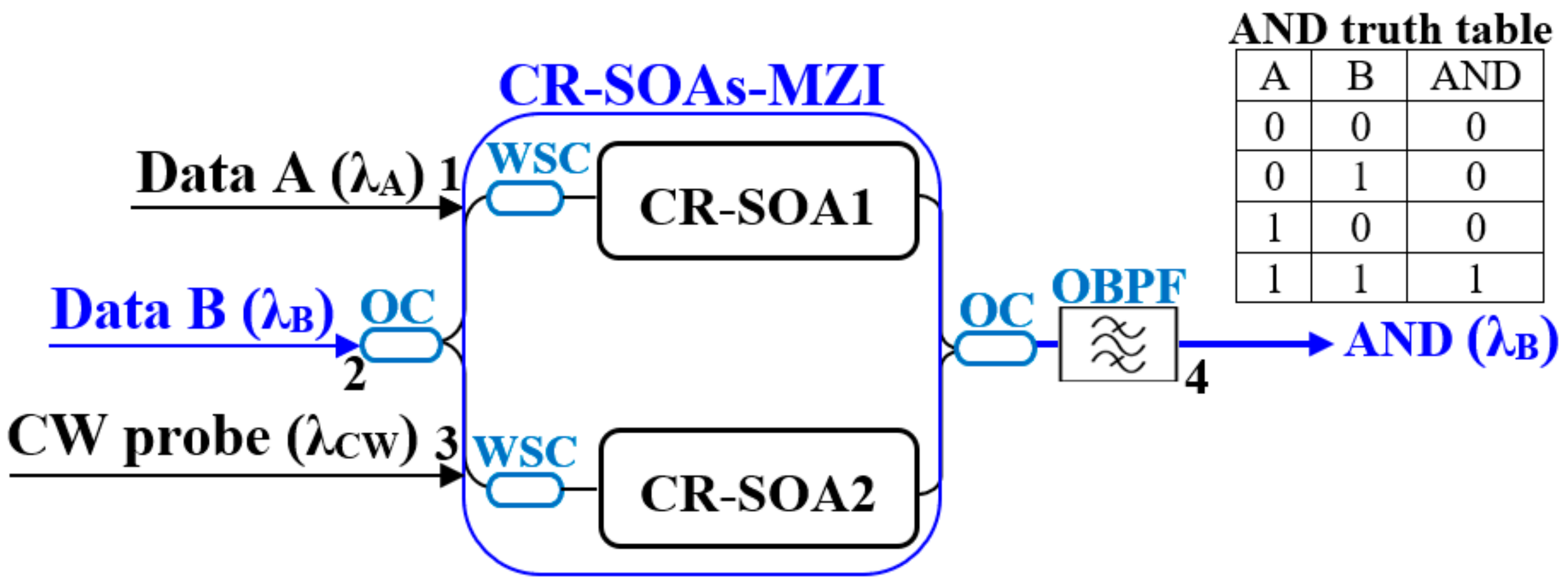
Figure 1. Schematic diagram illustrating the states and carrier transitions of CR-SOA [9,11,14].
Photonics 11 00648 g001
Figure 2. Diagram and truth table utilizing CR-SOAs-MZI as an AND gate.
Photonics 11 00648 g002
Figure 3. Diagram and truth table for 2x1 MUX using CR-SOAs-MZIs.
Photonics 11 00648 g003
Figure 4. AND gate outputs of the 2x1 MUX using CR-SOAs-MZIs at 120 Gb/s: (a) signal A, (b) signal S, (c) AND1 output, (d) AND1 eye diagram achieving QF = 27.71, (e) signal B, (f) inverted signal S, (g) AND2 output, and (h) AND2 eye diagram achieving QF = 21.53.
Photonics 11 00648 g004
Figure 5. 2x1 MUX using CR-SOAs-MZIs at 120 Gb/s: (a) signal A, (b) signal B, (c) signal S, (d) MUX output, and (e) MUX eye diagram achieving QF = 8.85.
Photonics 11 00648 g005
Figure 6. QF versus (a) pulse energy (E0) and (b) pulse width (τFWHM) for the 2x1 MUX using CR-SOAs-MZIs at 120 Gb/s.
Photonics 11 00648 g006
Figure 7. QF versus (a) injection current (I) and (b) saturation power (Psat) for the 2x1 MUX using CR-SOAs-MZIs at 120 Gb/s.
Photonics 11 00648 g007
Figure 8. QF versus (a) operating data rate and (b) selector signal power (PS) for the 2x1 MUX using CR-SOAs-MZIs at 120 Gb/s.
Photonics 11 00648 g008
Figure 9. QF versus amplified spontaneous emission (ASE) power for the 2x1 MUX using CR-SOAs-MZIs at 120 Gb/s.
Photonics 11 00648 g009
Table 1. Standard values for numerical parameters [1,2,3,4,5,6,7,8,9,10,11,12,13,14,15,16].
SymbolDefinitionValueUnit
E0Pulse energy0.8pJ
τFWHMPulse width1ps
TBit period8.33ps
KPRBS length127-
λASignal A wavelength1550nm
λBSignal B wavelength1550nm
λCWCW wavelength1550nm
λSSelector wavelength1500nm
PASignal A power1dB
PBSignal B power1dB
PCWCW power0dB
PSSelector power1dB
IInjection current300mA
PsatSaturation power30mW
τcCarrier lifetime200ps
τtTransition lifetime from CR to AR5ps
ηPopulation inversion factor0.3-
α α-factor5-
αCH CH linewidth enhancement factor1-
αSHBSHB linewidth enhancement factor0-
εCH CH nonlinear gain suppression factor0.1W−1
εSHBSHB nonlinear gain suppression factor0.1W−1
τCHTemperature relaxation rate0.3ps
τSHBCarrier-carrier scattering rate0.1ps
ΓConfinement factor0.3-
ɑ Differential gain10–20m2
NtrTransparency carrier density1024m−3
LAR length500μm
dAR thickness0.3μm
wAR width3μm
G0Unsaturated power gain30dB
NSPSpontaneous emission factor2-
υOptical frequency193.55THz
B0Optical bandwidth2nm
Reduced Planck’s constant1.05 × 10−34J·s
Table 2. Comparison of MUX logic gates based on different technologies.
SchemeData Rate (Gb/s)MetricReference
SOAs-MZI60QF > 6[1]
PhCs-CR = 18.53 dB[2]
PhC ring resonators310CR = 21.39 dB[3]
Titanium-diffused lithium> 40
niobate electro-optic MZI CR > 26 dB[5]
CR-SOAs-MZI120QF = 8.85This work
Disclaimer/Publisher’s Note: The statements, opinions and data contained in all publications are solely those of the individual author(s) and contributor(s) and not of MDPI and/or the editor(s). MDPI and/or the editor(s) disclaim responsibility for any injury to people or property resulting from any ideas, methods, instructions or products referred to in the content.