Article

Control of Single-Phase Electrolytic Capacitor-Less Isolated Converter for DC Low Voltage Residential Networks

1
Instituto Superior Técnico, University of Lisbon, 1049-001 Lisbon, Portugal
2
INESC-ID, 1000-029 Lisboa, Portugal
3
Instituto Superior de Engenharia de Lisboa, Polytechnic Institute of Lisbon, 1959-007 Lisboa, Portugal
*
Author to whom correspondence should be addressed.
Electronics 2020, 9(9), 1401; https://doi.org/10.3390/electronics9091401
Submission received: 31 July 2020 / Revised: 24 August 2020 / Accepted: 27 August 2020 / Published: 29 August 2020

Abstract

:
In recent years, there has been a desire to improve electricity generation and consumption, to reach sustainability. Technological solutions today allow a rational use of electricity with good overall performance. Traditionally, from production to distribution, electrical energy is AC-supported for compatibility reasons and easy voltage level transformation. However, nowadays most electric loads need DC power to work properly. A single high-efficiency central AC-DC power converter may be advantageous in eliminating several less efficient AC-DC embedded converters, distributed all over a residential area. This paper presents a new single-phase AC-DC converter using one active bridge (most isolated topologies are based on the dual active bridge concept) and a high-frequency isolation transformer with low-value non-electrolytic capacitors, together with its control system design. The converter can be introduced into future low-voltage DC microgrids for residential buildings, as an alternative to several embedded AC-DC converters. Non-linear control techniques (sliding mode control and the Lyapunov direct method) are employed to guarantee stability in the output DC low voltage with near unity power factor compensation in the AC grid. The designed converter and controllers were simulated using Matlab/Simulink and tested in a lab experimental prototype using digital signal processing (DSP) to evaluate system performance.

1. Introduction

In a growing and economically interconnected society, the availability of energy enhances economic growth. Besides the scarcity of natural energy resources, such as oil and coal [1], the use of these non-renewable energy sources might contribute to climate change. Several strategies have been deployed to encourage the use of renewable resources in a sustainable way, ensuring diversity and viability using environmentally friendly energy systems, with quality, safety and attractive costs to the final consumers [2,3]. Using clean and renewable energies in generation, combined with efficient end-use equipment, significantly contributes to reduce environmental pollution problems. Decentralized energy production (photovoltaic panels and wind turbines) reduces transmission energy losses, as energy transmission system losses increase when consumption is far from the generation units. Solar photovoltaics (PV) and wind turbines produce energy with different voltage levels at direct current or alternating current. This implies their adaptation using electronic power converters to enable the connection to local home networks or even to utility main networks. These networks are typically in AC with well-defined and standardized characteristics.
Modern equipment in the residential environment needs a direct current to perform properly, such as lighting systems, small appliances, mobile devices, air conditioning systems and, more recently, the charger systems for electric mobility devices. Battery chargers have a significant weight in modern residential electrical systems, as the amount of energy that they have to deal is significant when compared to the remaining equipment at home. In terms of energy savings, DC networks present a better overall efficiency compared to the traditional AC networks [4]. Even if it is necessary to adapt the voltage levels, the DC-DC converter is simple and efficient compared to the typical AC-DC converters.
With the recent progress in semiconductor technologies, for example, Gallium Nitride (GaN) high-electron mobility transistors (HEMT) or Silicon Carbide (SiC) Metal Oxide Field Effect Transistors (MOSFETs), a single high-efficiency central AC-DC converter could be advantageous in eliminating several less reliable and less efficient AC-DC embedded converters. In DC networks, there is no reactive power compensation, no need to synchronize generators to the network frequency, no skin effect and easier power failure mitigation if combined with energy storage systems [5]. To achieve better energy efficiency, domestic equipment such as refrigerators, washing machines and similar appliances, needing electrical machines, should use high-efficiency electrical machines (permanent magnet synchronous machines (PMSM)), which normally implies the use of built-in electronics to meet the requirements of high energy classification. PMSMs cannot be directly connected to an AC network and therefore converters are mandatory, unlike in traditional electric machines (asynchronous induction machines).
To ensure the equipment’s operating requirements, the choice of voltage level on the DC bus is a crucial factor to achieve energy efficiency. The DC network distribution system presents implementation challenges that have yet to be standardized in the domestic case [6]. The voltage level to be adopted on the DC bus should be selected, as a low DC voltage will require high currents for a given power, increasing the losses or the need to use costly section cables [7]. It is necessary to choose a voltage high enough to satisfy most loads without significantly increasing the current in the cables, while maintaining the safety in the electrical system. Consensus exists on using the level around 400 Vdc to cover different types of loads, mainly electric vehicles and their requirements, a value advocated by associations of equipment producers, which may possibly be adopted in the new regulations for the residential and commercial DC distribution networks [8]. For example, the Emerge Alliance’s [9] standards recommend 24 Vdc for the occupied space standard (low-power appliances and lighting, typically in bedrooms and living rooms, guaranteed safety and efficiency at lower voltage) and 380 Vdc for the data and telecom center standard (high-power loads, kitchen appliances, air conditioning systems for residential air conditioning and electric vehicles). Values in the order of 48, 120 and 230 Vdc have also been considered [10]. Well-accepted DC systems are the USB sockets already common in modern residential installations and office spaces. Its standardized version 3.1 can supply small loads up to 100 W [11]. In residential distribution systems, there are also systems that adopt two voltage levels in DC and systems called hybrids with the possibility of coexisting with both AC and DC systems to satisfy certain equipment requirements. In virtually all these cases, the connection to an electric power supplier is normally done to an AC distribution network. This connection implies the use of at least one electronic AC-DC converter with power factor compensation to meet the strict requirement of grid compatibility, safety and power quality standards [12].
The AC-DC converters with power factor compensator (PFC) characteristics can be classified as isolated and non-isolated. The non-isolated topologies in their simplest version are classified according to the use of complete rectifier diode bridges. When a topology does not require one or more diode bridges, it is recognized as bridgeless [13]. In this case, they generally exhibit better performance due to the reduced number of semiconductor elements. Isolated topologies present an extra protection against direct and indirect electric shocks because the phase wire is never directly connected to the output DC bus, offering galvanic isolation. This topology is preferred when it is needed to connect several sources and different loads. Typically, in isolated converters, transformers are used that can operate at relatively high frequency, which means a reduction in the manufacturing cost, size and weight of the transformer and entire converter. Power converters can also be classified as unidirectional and bidirectional due to the direction of the energy flow [14,15,16,17].
Considering the choice of topology for a central converter to feed the DC network in conjunction with other converters distributed in the network, inherent to the end-use devices, the entire system presents an estimate of energy savings of up to 5% in the case of non-storage systems and up to 14% when combined with storage systems [18,19]. In more optimistic scenarios, it can reach an energy saving of around 30% [20,21,22].
Most topologies use passive elements in their essence that act as filters for harmonic content caused by the switching of the semiconductors and, in the particular case of single-phase converters, the occurrence of ripple at the double of the line frequency in the output current, which can cause instability in the dc network [23]. This problem is usually solved by adding extra capacity value to the output filter or is naturally diminished when connected directly to batteries when there is energy storage. However, in both cases they suffer from dynamic stress caused by the ripple of the current. As a consequence, the useful lifetime of capacitors (usually electrolytic) or batteries is reduced. Currently, there has been interest in studying alternatives for reducing the value of capacitors’ output and using capacitors with greater efficiency, such as film or ceramic capacitors, for power decoupling and achieving better results when combined with the appropriate control techniques [12,23,24]. The addition of dynamic voltage restorers or active power decoupling are discussed in [25], with the advantage of improving energy efficiency and reducing the ripple of the output voltage.
There are several topologies for AC-DC isolated converters with PFC characteristics using different control techniques as described in [26]. Several topologies are derived from solid-state transformers [27] and from DC-DC converters for a low-voltage direct current (LVDC) [28]. Non-linear control techniques applied in LVDC residential microgrids are described and compared in [28,29]. Non-linear controllers range from feedback linearization, used to guarantee robustness against parameter changes [28], to hysteresis current controllers for the inner loop and Lyapunov stabilized non-linear output DC voltage controller [29]. References [28,29] also present comparisons to several alternative linear and non-linear controllers, both references reaching the conclusion that linear feedback controllers show lower performance in LVDCs with constant power loads, when compared to sliding mode and Lyapunov stabilized methods [28,29]. However, the non-linear controllers presented in [28,29] were applied to simple DC-DC buck non-isolated converters. This paper proposes sliding mode and the use of quadratic quantities to achieve linearization and Lyapunov stability methods for the AC-DC isolated converter herein proposed. High- and low-frequency dynamics are separated, and an integral term is added in the internal current controller to guarantee zero steady-state error and robustness against parameter variation.
For the implementation of control systems, currently the preferred choice is to use digital control for the rapid development prototypes in power electronics converters with strict real-time control restrictions at low cost. In addition, a fast processing capacity is also required as a fast response at the peripheral level, such as signal conditioners (voltage and current demands) and semiconductor drivers, especially in control loops with critical times. The pulse modulation signals (PWM) are generated directly from the digital unit control system without a specific hardware specification requirement. Digital signal processors (DSPs) are commercially available and specifically designed to control electronic power converters and software tools for rapidly developing applications for real-time control systems, including all the peripherals normally needed for this type of application in a single chip.
This paper presents and designs the converter topology and the digital control system for a single-phase AC-DC converter using a high-frequency isolation transformer with low-value non-electrolytic capacitors to be introduced into a future low-voltage DC network in residential buildings, as an alternative to traditional AC networks. Sliding mode control and Lyapunov direct stability method control are employed in the proposed converter to guarantee stability and disturbance robustness to the output DC low-voltage network with power factor compensation to the main utility AC grid.
This paper introduces three main contributions. First, the circuit topology using one active bridge with the ability to control the current of the main AC grid and at the same time manage the energy flow to the output LVDC side, using a low-capacity intermediate DC bus, presenting a different alternative to the typical isolated dual active bridge (DAB). Second, the control strategy assumes the converter dynamics can be separated, then uses non-linear approaches, such as sliding mode and the Lyapunov second method of stability, to step back the control from the DC output to the AC 50 Hz input current that interfaces the DC nanogrid to the AC grid, using square quantities. To prevent the effects of measuring errors and parameter mismatch, the input current non-linear controller includes an integral term. An internal auxiliary control ensures the AC high-frequency voltage in the isolating transformer has zero average value. Third, a new approach is used to reduce dynamic current stress caused by the natural 100 Hz ripple output, using low-valued film capacitors, presented as an alternative to the voltage restored and voltage drop compensators, based on high-valued electrolytic capacitors.
The designed controller performance was simulated using Matlab/Simulink and an experimental prototype is implemented using a low-cost DSP (TMS320F28379D) from Texas Instruments to verify and evaluate the performance of the proposed control.

2. Converter Model and Control

2.1. Description of the Proposed Converter

The proposed topology of the single-phase AC-DC converter with a high-frequency transformer, power factor compensation and low-distortion AC input current is depicted in Figure 1 to provide energy to a DC low-voltage network. The proposed converter is unidirectional with active power decoupling at the output to significantly reduce the capacitor value of the DC voltage bus. This circuit is composed of one inductor L S at the input connecting to the main AC utility grid u S . After the input inductor, a full-bridge rectifier containing four diodes, D 1 , D 2 , D 3 and D 4 , and a capacitor C 1 , with the function of rectifying the input current and at the same time filtering the harmonic content of the current i R 1 caused by the switching of semiconductors, S 1 , S 2 , S 3 and S 4 , assembled in a full-bridge inverter topology based in GaN-controlled high-electron mobility transistors (HEMT) (GS66516B).
The inverter is connected to the transformer primary ( u T 1 ), with the purpose to generate a high-frequency alternating current i T 1 for the transformer and simultaneously control the voltage u C 1 at capacitor C 1 . On the secondary side ( u T 2 ), a high-frequency diode full-bridge rectifier, D 5 , D 6 , D 7 and D 8 feed the output boost-type converter with inductor L 0 , capacitor C 0 and one GaN HEMT device S 5 (GS66516B) and diode D 9 , with the function of reducing the ripple in the output voltage u 0 and reducing the value of capacitor C 0 .
Converter modeling can be obtained considering that all semiconductors’ devices are ideal, while neglecting the losses of the inductors and capacitors. The semiconductors’ states can be represented by switching variables δ 1 ( t ) , (1), and δ 2 ( t ) , (2), supposing ideal HEMTs.
Switching variables δ 1 ( t ) and δ 2 ( t ) are the control inputs, while the control outputs are the output voltage u 0 and the amplitude of the quasi-sinusoidal (low-distortion) AC input current i L s . As the output is DC, and the input i L s is AC 50 Hz, while the intermediate inverter/transformer operates at a high switching frequency (kHz), the control strategy is devised supposing the three different converter dynamics associated with DC, 50 Hz and kHz can be separated.
δ 1 ( t ) = { + 1 ( S 1 ,   S 4     O N ) 0 ( S 1 ,   S 3     O N   o r   S 2 ,   S 4     O N ) 1 ( S 2 ,   S 3   O N )
δ 2 ( t ) = { 0 ( S 5   O N ) 1 ( D 9     O N )
Therefore, the control strategy starts with the tracking of the output voltage u 0 to define δ 2 ( t ) , supposing a regulated value i L 0 > 0 . Then, the control design progresses to define the needed reference value of the AC input current i L s , using the converter input–output power balance. As the switching variable δ 1 ( t )   is useful to impose the u C 1 voltage, then the necessary u C 1 voltage is computed so that the AC 50 Hz input i L s tracks the i L s r e f reference value. The necessary u C 1 voltage to enforce the i L s current is then tracked using   δ 1 ( t ) . In Figure 2, the simplified control scheme for the proposed isolated AC-DC converter is presented.

2.2. Sliding Mode Control for Voltage u 0

Supposing continuous conduction mode ( i L 0 > 0 ), the dynamic model (3) of voltage u 0 can be obtained from the circuit analysis by applying Kirchhoff laws to the circuit in Figure 1.
d u 0 d t = 1 C 0 ( ( 1 δ 2 ( t ) ) i L 0 i 0 )
The first-time derivative of u 0 contains the control action δ 2 ( t ) , thus the strong relative degree of u 0 is one [30], and a suitable sliding surface can be obtained as a linear combination of the control error e u 0 = u 0 r e f u 0 , where u 0 r e f is the reference value to be tracked by the u 0 voltage. Considering a positive gain k 1 , valued to bound the semiconductors’ switching frequency, a suitable sliding surface is defined by S ( e u 0 , t ) = k 1 e u 0 = Δ u 0 0 [30,31,32,33,34,35]. The switching strategy is achieved by applying the sliding mode stability condition S ( e u 0 , t ) S ˙ ( e u 0 , t ) < 0 . The sliding surface derivative S ˙ ( e u 0 , t ) is given in (4).
S ˙ ( e u 0 , t ) = k 1 ( d u 0 r e f d t ( 1 δ 2 ( t ) ) i L 0 i 0 C 0 )
From (4), to ensure stability, the control strategy is defined in (5).
{ i f   S ( e u 0 , t ) > 0 ,   then   S ˙ ( e u 0 , t ) < 0 d u 0 r e f d t ( 1 δ 2 ( t ) ) i L 0 i 0 C 0 < 0 i f   S ( e u 0 , t ) < 0 ,   then   S ˙ ( e u 0 , t ) > 0 d u 0 r e f d t ( 1 δ 2 ( t ) ) i L 0 i 0 C 0 > 0
It is necessary to satisfy the inequalities in (5) to guarantee the sliding mode stability, giving the reaching condition written in (6).
δ 2 ( t ) i L 0 C 0 > M A X ( i L 0 i 0 C 0 d u 0 r e f d t )
To impose a finite switching frequency, the ripple Δ u 0 voltage must be considered and k 1 selected to ensure stability and a fast response. From (5), the control law in (7) defines the value of the switching variable δ 2 ( t ) .
{ i f   S ( e u 0 , t ) > Δ u 0 2 ,   t h e n     S ˙ ( e u 0 , t ) < 0           δ 2 ( t ) = 0 i f   S ( e u 0 , t ) < Δ u 0 2 ,   t h e n   S ˙ ( e u 0 , t ) > 0   δ 2 ( t ) = 1
The reaching condition is verified by assuming the current i L 0 as an independent source, with the value imposed by another controller doing i L 0 r e f = i 0 k 2 and considering k 2 > ( 1 + Δ i L 0 2 i 0 ) with Δ i L 0 , the double AC network frequency current ripple. The control law (7) is not dependent on system parameters or quantities other than the controlled quantity, ensuring the control loop robustness.

2.3. Control Using the Lyapunov Direct Method of Stability to Obtain the Reference for Current i L s r e f ( t )

Analysing the circuit presented in Figure 1, the dynamic model for the current i L 0 is (8), where the switching variable δ 2 ( t ) is also present. However, it cannot be used as a control input as it is already in use to control the u 0 output in (7).
d i L 0 d t = 1 L 0 ( u r 0 ( 1 δ 2 ( t ) ) u 0 )
As u r 0 is not a state variable, it cannot be used as a virtual control input. To choose a virtual control input from one AC input state variable, the converter input–output power balance is applied. Therefore, assuming, as system parameters, the efficiency η of the converter, the power P S at the AC network, the power P u r 0 at the diode full-bridge rectifier, D 5 , D 6 , D 7 and D 8 , P u r 0 = i L 0 u r 0 = U s r m s I L s r m s η , then the output inductor L 0 current is i L 0 = i 0 / ( 1 δ 2 ( t ) ) , . The delivered output power P 0 = i 0 u 0 , is given as P 0 = i L 0 ( 1 δ 2 ( t ) ) u 0 . Therefore, the linear dynamic model (9) is received from (8), where the control variable i L 0 2 is the square of i L 0 and the control input is the state variable AC current I L s r m s .
d i L 0 2 d t = 2 L 0 ( U s r m s I L s r m s η P 0 )
Consider the model (9) and define the control objective to be e i L 0 2 = 0 , the tracking error being e i L 0 2 = i L 0 r e f 2 i L 0 2 . To guarantee zero steady-state error, even when the efficiency η and the delivered output power P 0 are unknowns, add the integral of the tracking error e 1 =   e i L 0 2 d t to ensure the convergence to the origin, in steady-state, even with non-modeled disturbances and parameter uncertainty. Choose a positive definite Lyapunov function V 2 with k 3 > 0 written in (10) [36].
V 2 = 1 2 k 3 e 1 2 + ( e i L 0 2 ) 2 2
From the Lyapunov direct method of stability, the time derivative of V 2 ( e i L 0 2 , t ) must be negative to guaranty stability. Therefore, as V 2 V ˙ 2 < 0 , then V 2 ˙ = k 4 ( e i L 0 2 ) 2 , k 4 > 0 , leading to Equation (11) from (9) and (10).
k 3 e 1 e i L 0 2 + e i L 0 2 ( d i L 0 r e f 2 d t 2 C 0 ( U s r m s I L s r m s η P 0 ) ) = k 4 ( e i L 0 2 ) 2
Knowing that i L s r e f = I L s r m s 2   s e n ( ω t + φ ) and considering (11), the virtual control equation for i L s r e f is a function of the output inductor current i L 0 r e f 2 :
i L s r e f ( t ) = L 0 2   s e n ( ω t + φ ) 2 η U s r m s ( k 3 e 1 + k 4 ( i L 0 r e f 2 i L 0 2 ) + 2 P 0 L 0 )
The k 3 and k 4 constants must be selected to obtain a slow enough response for the input AC current i L s r e f in order to avoid harmonic distortion in the input current i L s . This condition enables the control using separated low-frequency and high-frequency dynamics.

2.4. Lyapunov Control for Current i L S to Track the Reference i L s r e f ( t )

It is intended to control the current i L S by applying again the Lyapunov direct method of stability to obtain a low THD i L S current and i L S in phase with the voltage u S for the unity power factor. The i L S r m s value is regulated according to the load power needs. Analyzing Figure 1, the dynamic model for current i L S considering the control variable u C 1 is written in (13), where s g n ( i L S ) u C 1 = u S 1 .
d i L S d t = 1 L S ( u S s g n ( i L S ) u C 1 )
From (13), the voltage u C 1 is the control input for the i L S current. To control i L S , u C 1 can be enforced to follow the reference u C 1 r e f , determined so that i L S = i L s r e f ( t ) . Defining the control objective e i L s = 0 , the tracking error is e i L S = i L s r e f i L s , and a candidate positive definite Lyapunov function can be selected as (14) to be V 1 ( i L s , t ) > 0 .
V 1 ( i L s , t ) = e i L s 2 2
The time derivative of V 1 ( e i L s , t ) must be negatively definite for all ( i L s , t ) , according to V 1 V 1 ˙ < 0 . Considering V 1 ˙ = k 5 e i L s , with k 5 > 0 ,   the virtual control u C 1 r e f in (15) is obtained considering also (13).
u C 1 r e f = s g n ( i L S ) ( u s k 5 L s ( i L s r e f i L s ) d i L s r e f d t L s )

2.5. Sliding Mode Control for Voltage u C 1 to Track the Reference u C 1 r e f

Analyzing the circuit presented in Figure 1, the dynamic model for voltage u C 1 is
d u C 1 d t = 1 C 1 ( | i L s | δ 1 ( t ) 2 i L 0 / n )
The first-time derivative of u C 1 contains the control action δ 1 ( t ) , thus the strong relative degree of u 0 is one [30], and a suitable sliding surface S 1 can be obtained as a linear combination of the control error e u C 1 = u C 1 r e f u C 1 where u C 1 r e f is the reference value to be tracked by the u C 1 voltage. Considering a positive gain k 6 , used to bound the semiconductors’ switching frequency, a suitable sliding surface is defined by S 1 ( e u C 1 , t ) = k 6 e u C 1 = Δ u C 1 0 [30,31,32,33,34,35]. The switching strategy is achieved by applying the sliding mode stability condition S 1 ( e u C 1 , t ) S ˙ 1 ( e u C 1 , t ) < 0 . The derivative of the switching surface is (17).
S ˙ 1 ( e u C 1 , t ) = k 6 ( d u C 1 r e f d t | i L s | C 1 + δ 1 ( t ) 2 i L 0 / n C 1 )
From (17), the control strategy is defined in (18).
{ i f   S 1 ( e u C 1 , t ) > 0 ,   t h e n   S 1 ˙ ( e u C 1 , t ) < 0 d u C 1 r e f d t | i L s | C 1 + δ 1 ( t ) 2 i L 0 / n C 1 < 0 i f   S 1 ( e u C 1 , t ) < 0 , t h e n   S 1 ˙ ( e u C 1 , t ) > 0 d u C 1 r e f d t | i L s | C 1 + δ 1 ( t ) 2 i L 0 / n C 1 > 0
To guarantee stability, it is necessary to satisfy the reaching condition (19).
δ 1 ( t ) 2 i L 0 / n C 1 > M A X ( | i L s | C 1 d u C 1 r e f d t )
To impose a finite switching frequency, the ripple Δ u C 1 voltage must be considered and k 6 selected to ensure a fast enough response. From (18), the robust control action (switching variable) for δ 1 ( t ) is given in (20).
{ i f   S 1 ( e u C 1 , t ) > Δ u C 1 2 ,   t h e n     S 1 ˙ ( e u C 1 , t ) < 0         δ 1 ( t ) = 0 i f   S 1 ( e u C 1 , t ) < Δ u C 1 2 ,   t h e n     S 1 ˙ ( e u C 1 , t ) > 0 δ 1 ( t ) = 1   o r   δ 1 ( t ) = 1
The condition (19) is satisfied mainly as long as i L 0 / n > | i L s | is verified.
To avoid magnetic saturation of the transformer core, an auxiliary control signal takes advantage of the redundancy presented in (20) to ensure transformer primary voltages with zero average value.

3. Simulation Results

Characteristics of the Converter

The proposed isolated converter topology for the AC-DC converter (Figure 1) is simulated using Matlab/Simulink software. The control block diagram and the power circuit are assembled in Simulink with SimPower Systems Toolbox. The simulation contains the semiconductor models, including the effects of switching and on-state losses. The parameters for simulations are presented in Table 1.
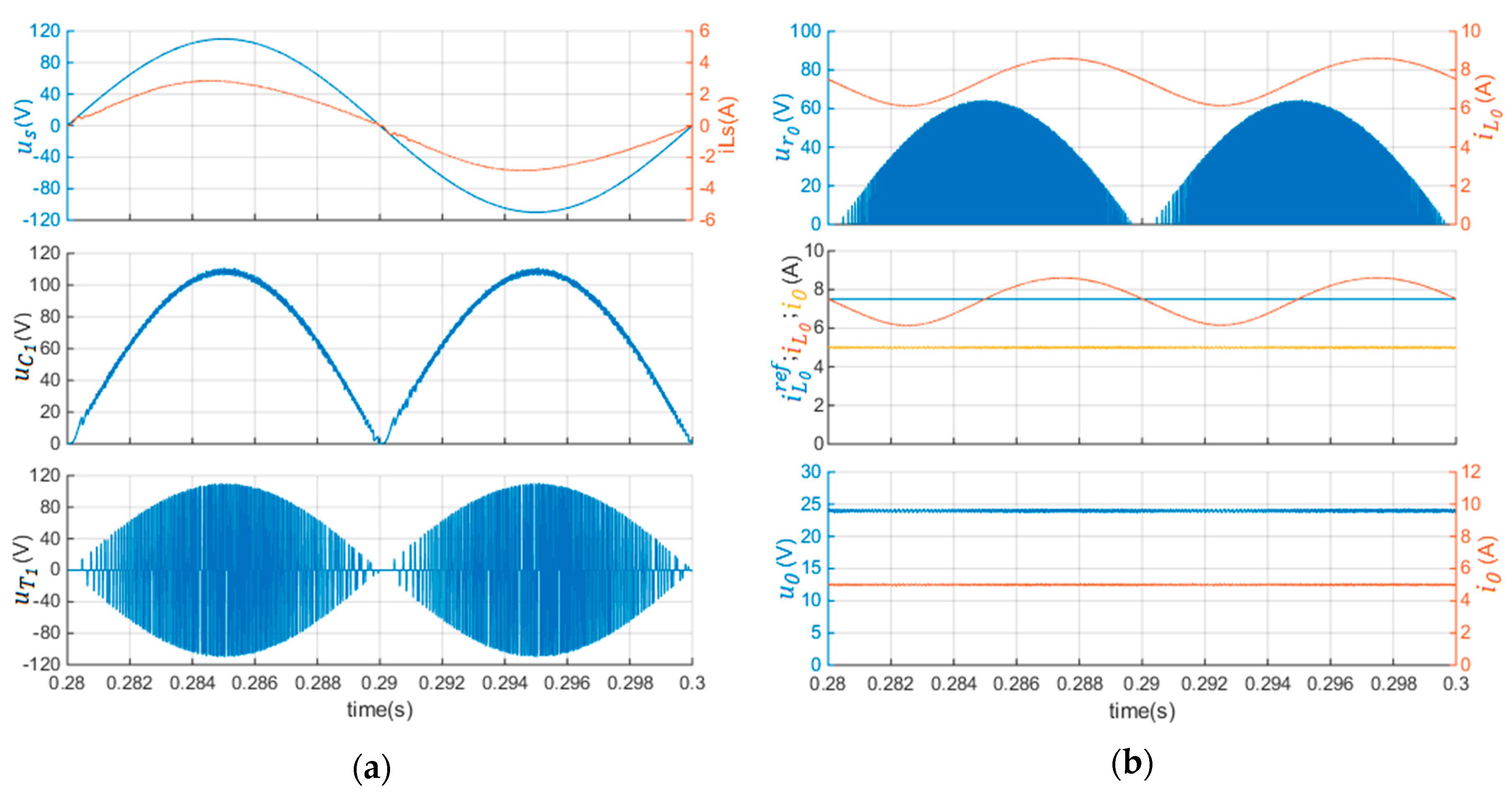
The simulation is performed at a given power in order to obtain results that can be compared with the experimental prototype developed in the laboratory. In addition, the calculation step in the simulation was adjusted to 5 µs to approximate the sample time of the control loop implemented in DSP, remembering that the loop time affects the switching frequency of semiconductors as the sliding mode controller will work at a slightly variable frequency determined mainly by the digital hysteretic comparators (7) and (20). Figure 3 represents the simulated waveforms of the main variables in the converter for one 50 Hz cycle of the AC power supply.
The simulation results show the performance of the converter controllers maintaining the current i L S in phase with the grid voltage u s (Figure 3a top). The output voltage is constant at 24 V besides the strong ripple in u R o and in i L 0 (Figure 3b top). The action of the internal loop controller u C 1 is responsible for imposing the capacitor C 1 voltage (Figure 3a middle), its double rectified shape, amplitude and phase relative to the voltage of the AC source to enforce the i L S current (see Section 2.5). The i L s control loop (see Section 2.4) generates the variable of the voltage reference u C 1 r e f necessary to obtain the desired main current at the input i L s with a low harmonic content.
In this simulation, it is also shown the possibility of achieving low total harmonic distortion for the i L S input current. In the MatLab analysis tool (FFT analysis), the obtained THD was 3.9% for i L s . The improvement in the reduction of the input current i L s THD, when compared to hysteresis current controllers, is due to the fact that the controllers first define a virtual control variable u C 1 (showing a higher ripple, Figure 3a middle) that indirectly enforces the input current via the second order input filter, instead of directly controlling the current i L s .
The control design uses sliding mode control in internal loops to offer robustness and a fast response with a slightly variable frequency, as (7) and (20) do not depend on system parameters. This robust implementation is nevertheless limited by the sample time.
The primary of the transformer is driven by the high-frequency voltage u T 1 (Figure 3a bottom) around 12 kHz at the maximum value of the amplitude of voltage u C 1 .
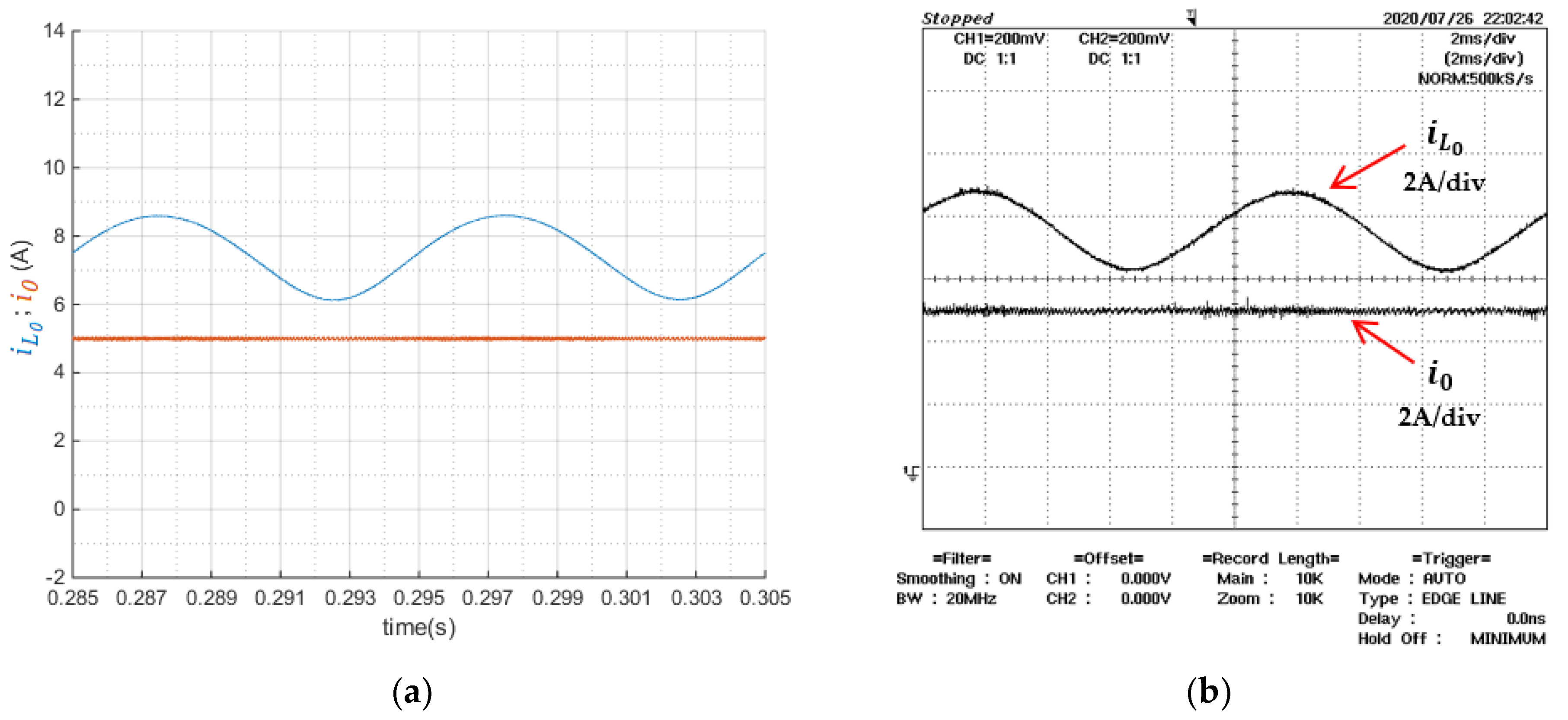
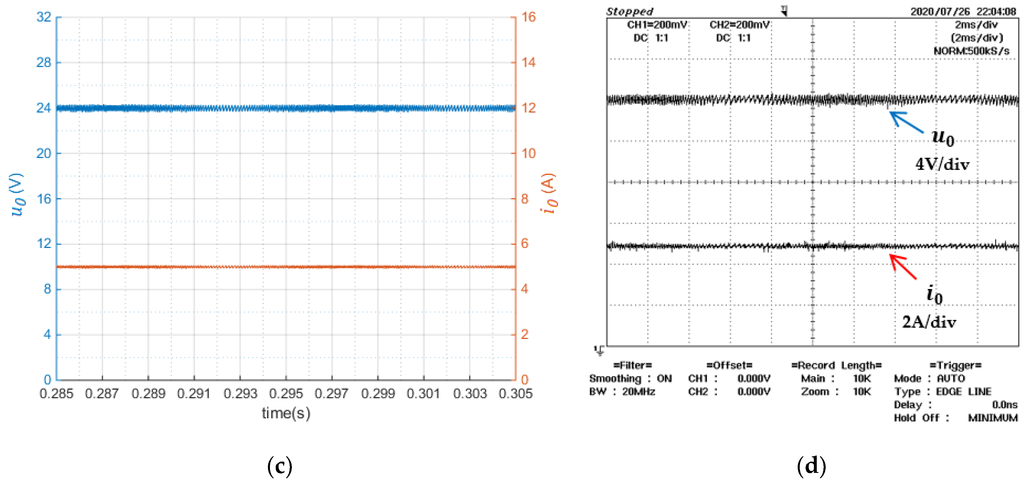
The transformer secondary side includes the high-frequency rectified voltage u r 0 and the waveform of the current i L 0 (Figure 3b top) presents the expected oscillation around its average value reference i L 0 r e f (see Section 2.3), as the AC power is not constant within an AC 50 Hz cycle, while the DC power may be constant. The load voltage u 0 (Figure 3b bottom) maintains a constant value over a period of the AC network as well as the current i 0 (see Section 2.2), according to the desired output power.
To evaluate the regulation of the converter output voltage, two simulations (Figure 4) are considered with different voltage values under the same conditions indicated in Table 1. For example, u 0 r e f = 12 V for server power supplies applications [37,38] and u 0 r e f = 28 V for aircraft avionics applications [39,40].
It is verified that the output load voltage remains constant over one cycle period of AC power. The current i L S stays in phase with the grid voltage u s identical to Figure 3a top with THD at 4.0% in both cases. The output voltage ripple u 0 (in blue) at 12 V and 28 V is the same ( Δ u 0 ≈ 0.6 V) due to the voltage-independent sliding mode controller.
Another simulation is made by considering a variation in the amplitude of the AC mains voltage (25%) with a duration time of 0.6 s (Figure 5 top) to check if the design converter and controller can supply the requested constant power load. The output voltage response is presented in Figure 5 bottom, revealing a perfectly controlled 24 V DC voltage.
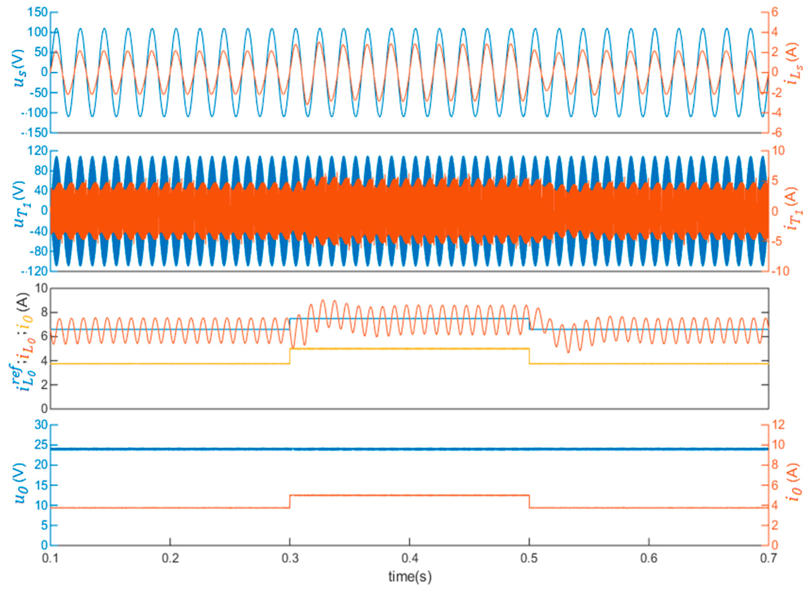
To test the performance of the proposed controller in transient conditions, 25% of the load nominal power changes are considered. Figure 6 presents the time evolution in transient conditions.
The presented results confirm that the proposed converter and control method maintains the power factor close to unity in transient conditions. The voltage applied at the transformer primary side presents symmetry and zero average value, using the redundancy present in the voltage control u C 1 (20), implemented in the auxiliary controller, to avoid core saturation of the high-frequency transformer.
At variable load conditions (adding a transient condition at time 0.2 s and removing at time 0.4 s) for a load step power increase of 25%, the output voltage u 0 shows in this case no voltage droop or perceptible voltage disturbances.

4. Experimental Results

4.1. Converter Prototype and Experimental Setup

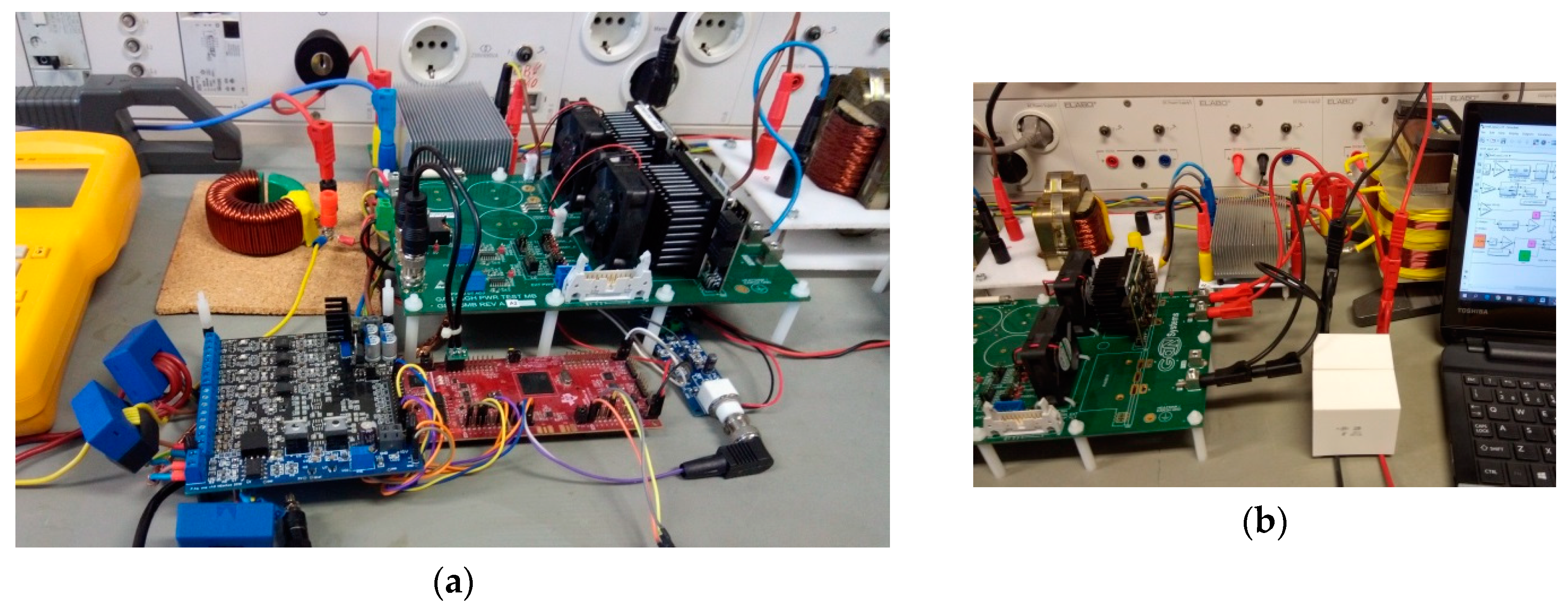
A prototype of the isolated AC-DC converter was built in the laboratory to experimentally evaluate the methodology of the proposed control technique. The prototype contains the main power converter, with component values shown in Table 1, and a digital control system. The prototype is connected to the laboratory low-voltage AC network using a single-phase auto-transformer. The converter primary side includes one full-bridge rectifying based on diodes VS-80APS12-M3 from Vishay and one board GSP65MB-EVB from GaN Systems with two GSP65R25HB-EVBs configured as a full-bridge inverter topology. The isolated high-frequency transformer was built using an iron base amorphous alloy from Metglas type 2605SA1 in size AMCC 32, designed for a maximum power of 3 kW and frequency up to 20 kHz with a 1.6:1 ratio. The converter secondary side includes a full-bridge high-frequency rectifier with diodes C5D50065D from Wolfspeed/Cree and one board GSP65MB-EVB from GaN Systems with one GSP65R25HB-EVB. To sample the needed currents, Hall effect sensors LA100-P/SP3 are used. Needed voltages are sampled using differential isolated amplifiers SI8920 from Silicon Labs. For the critical u C 1 voltage control loop, one differential probe was used with high input impedance developed to connect to the DSP (based in LMH6609MF from Texas Instruments), to reduce the delay time in the voltage reading process, when compared to the isolated SI8920.
A picture of the experimental prototype workbench benchmark is depicted in Figure 7.
The digital control circuit is composed of the Texas Instruments DSP model Delfino MCU TMS320F28379D launchpad development kit which features a 200 MHz dual core microcontroller (Core 1 and Core 2) and dual real-time control co-processors (CLA), a 32-bit floating point, 12/16 bits ADCs at 3.5/1.1 MSPS, comparators, PWM and other peripherals which boost rapid prototyping development. All algorithms are programmed in the MatLab/Simulink environment using the toolbox embedded coder support package for TI C2000. The digital algorithm was debugged in the Simulink environment and the code automatically generated and downloaded to the development TI DSP board.

4.2. Digital Control Implementation

To implement the control algorithms obtained in Section 2 in the TI DSP, the block diagram capabilities of Simulink using the C2000 Embedded Target Library were used. The Simulink C2000 Target Library includes models and algorithms for the specific peripherals of the TI DSP.
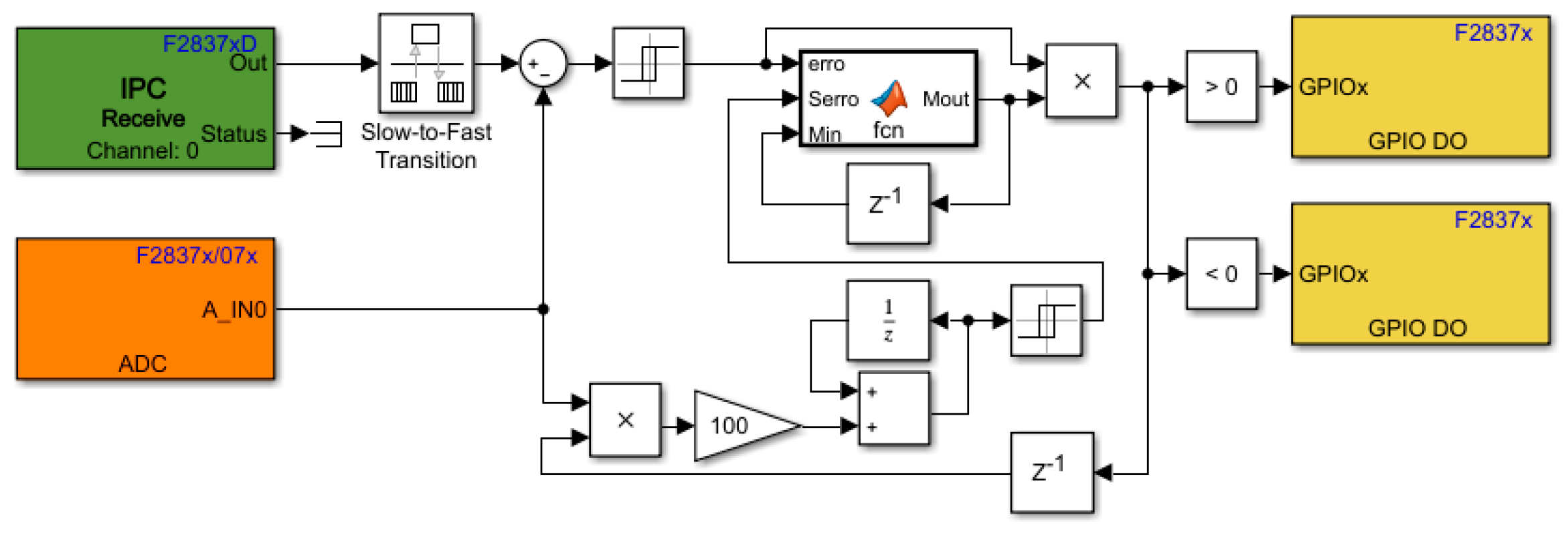
The critical voltage control loop of the capacitor voltage u C 1 was the first digital control loop to be developed. It was implemented in Core 1, used just for that purpose, with a 5 µs sample time. The digital algorithm was optimized by selecting suitable discrete Matlab functions, function calls or using convenient data types. The digital control (Figure 8) block diagram performs the sampling of the ADC of voltage u C 1 . Then, it compares the sampled u C 1 to the reference u C 1 r e f   (Section 2.5), which is received from Core 2 using the IPC receive block. To avoid core saturation of the high-frequency transformer, an auxiliary control loop is included. It uses a digital integrator and comparator to compute a running average of the transformer primary voltage. The control outputs are the digital signals to command the gates’ drivers of full-bridge GaN HEMTs (Figure 8).
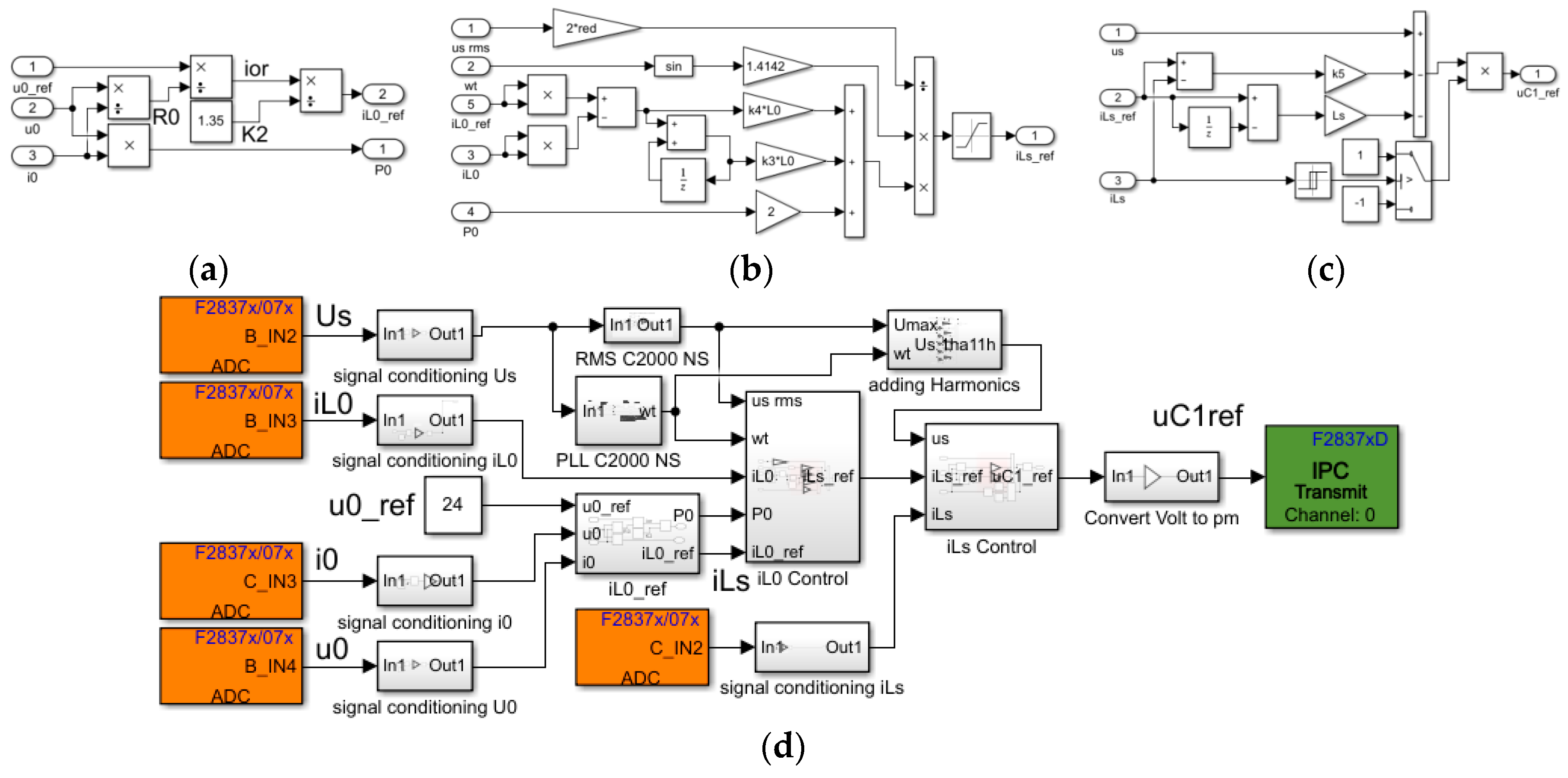
Core 2 was used to program the remaining controllers (Figure 9a–c), the control laws obtained in (7), (12) and (15) respectively relating to controls for u 0 , i L 0 and i L s . The sampling period is 50 µs. Programming using explicitly the two Cores has the advantage of reducing the time implementation of the models, which is essential for high-frequency converters. In addition, other common MatLab blocks can be used, as long as they are discrete block sets with special IQ math and motor control blocks located in the optimization subgroup, including Clark transformation, Park transformation, speed measurement and space vector generator and more. For the output voltage controller u 0 , another auxiliary DSP with the same characteristics is used for implementing the algorithms of Section 2.2, working independently.

4.3. Lab Prototype Results

Simulation and experimental results are compared and presented in Figure 10, Figure 11 and Figure 12, illustrating the operation of the AC-DC isolated converter controller by the TI DSP under Table 1’s conditions.
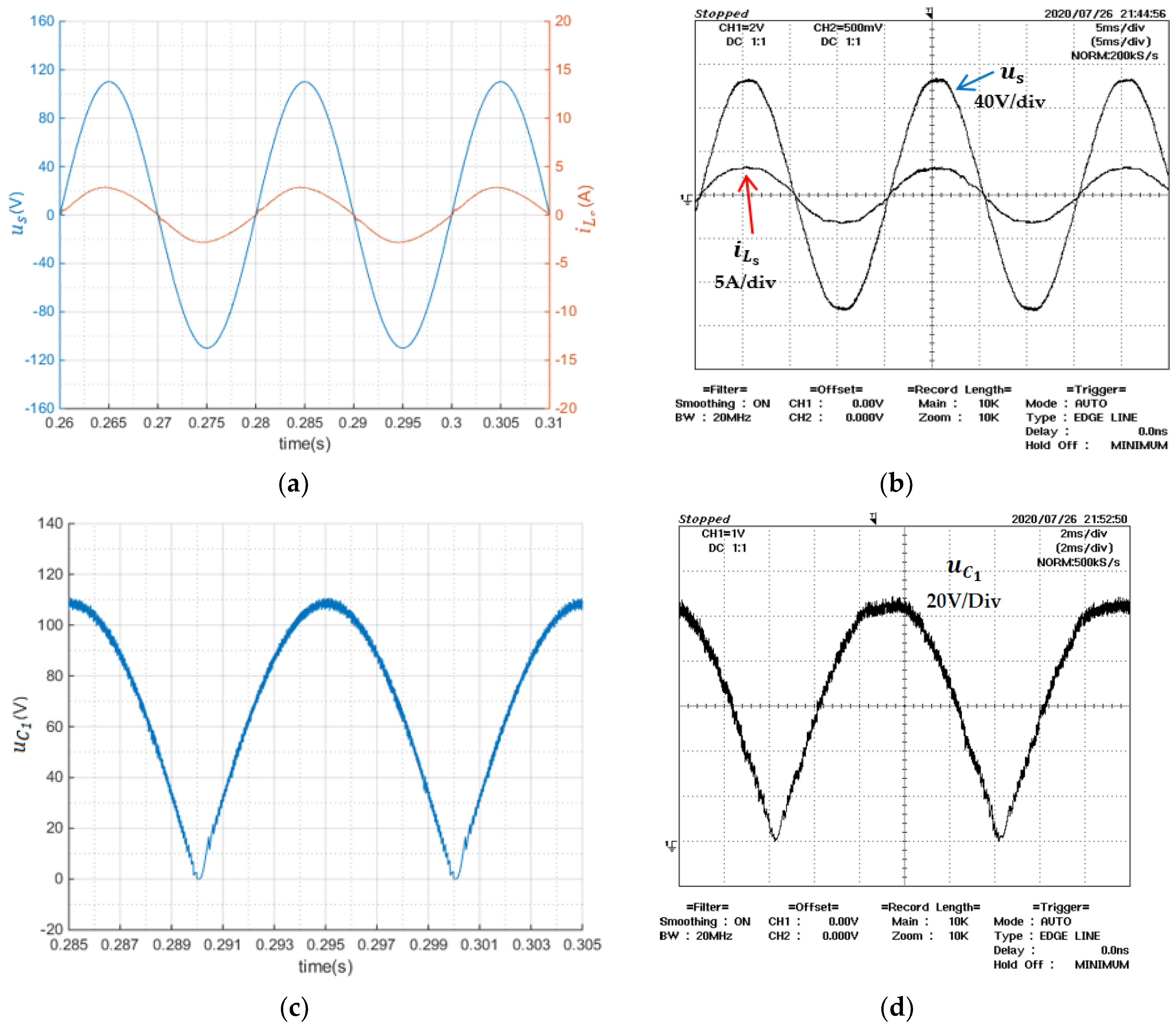
Figure 10a presents the simulation waveform of the main AC utility grid with a voltage u s of 110 Vpeak (0% of THD). A current i L S of 2.85 Apeak was obtained with 3.9% of THD measured using the FFT analysis tool in MatLab. For comparison, the experimental result is illustrated in Figure 10b, where the waveform of the main AC utility grid voltage u s with 104 Vpeak (1.4% of THD) is presented, as well as the waveform of the current i L S with 3.0 Apeak. The current i L S has a near sinusoidal shape with 4.7% of THD (all experimental THD values were measured with a Fluke 39 power meter).
Figure 10d shows the time evolution of the capacitor voltage u C 1 during one period of the mains grid with the high frequency ripple (maximum 24 kHz) characteristic of the non-linear control systems measuring 6 V of ripple of u C 1 , while in the simulation, 5 V was obtained as illustrated in Figure 10c. The difference in these values is due to the finite step-time for the simulation and the digital processing time for the experiments (both set to 5 µs), but experimental results have an extra delay time (1 µs) due to the delay of circuits measuring voltage u C 1 . Figure 10e depicts the time behaviour of current i L S and shows also the symmetry of the voltage u T 1 applied to the primary of the transformer, with the zero average value avoiding core saturation (detailed in the Figure 11a). The experimental results shown in Figure 10f closely match the simulation results of Figure 10e.
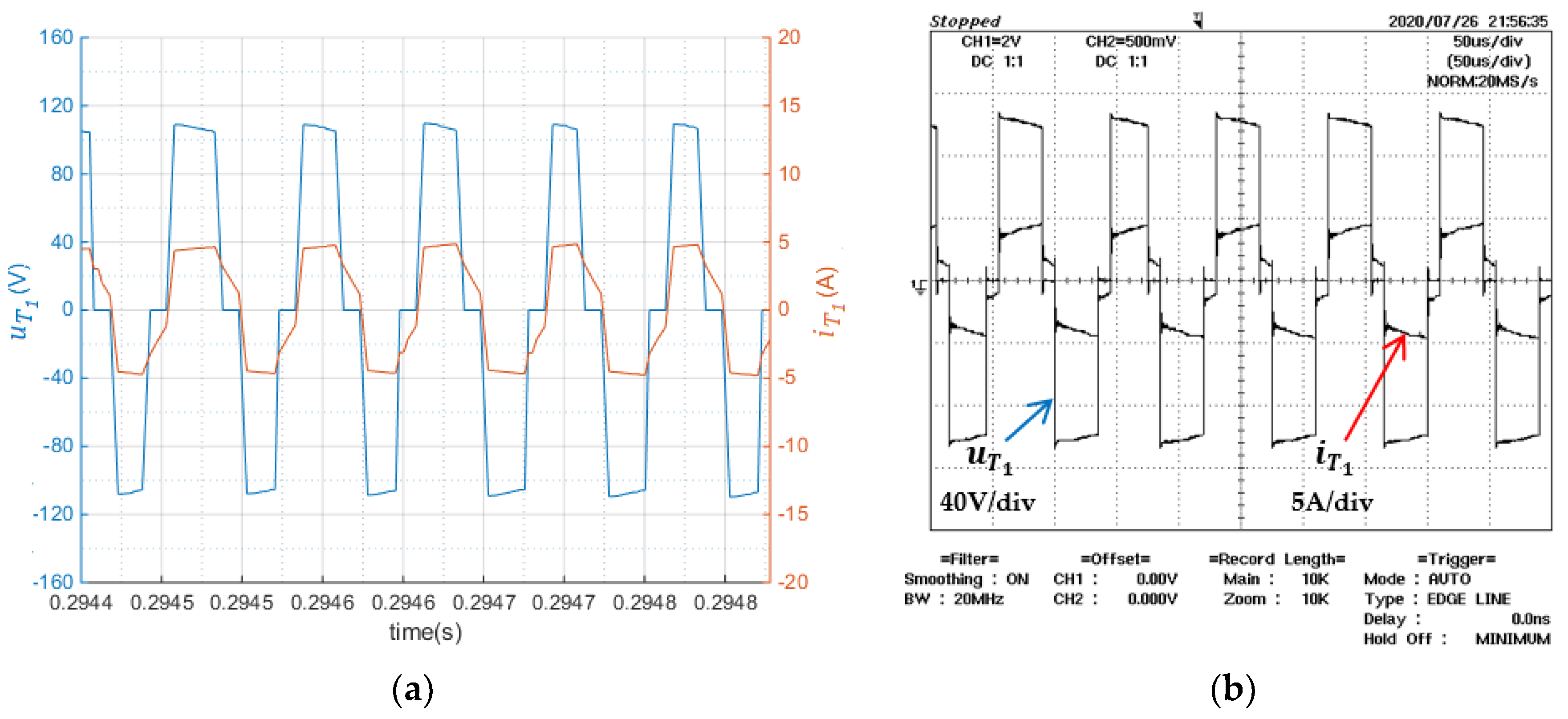
Figure 11b shows, in detail, the experimental result of switching the voltage u T 1 and the current in the primary of the high-frequency transformer at the maximum voltage amplitude situation. The waveform voltage and current present a near rectangular shape with a variable frequency and duty cycle, due the control technique, reaching around 12 kHz in this case, which differs to the values measured in the simulation results (Figure 11a), which are around 14 kHz due to the u C 1 voltage measuring delay.
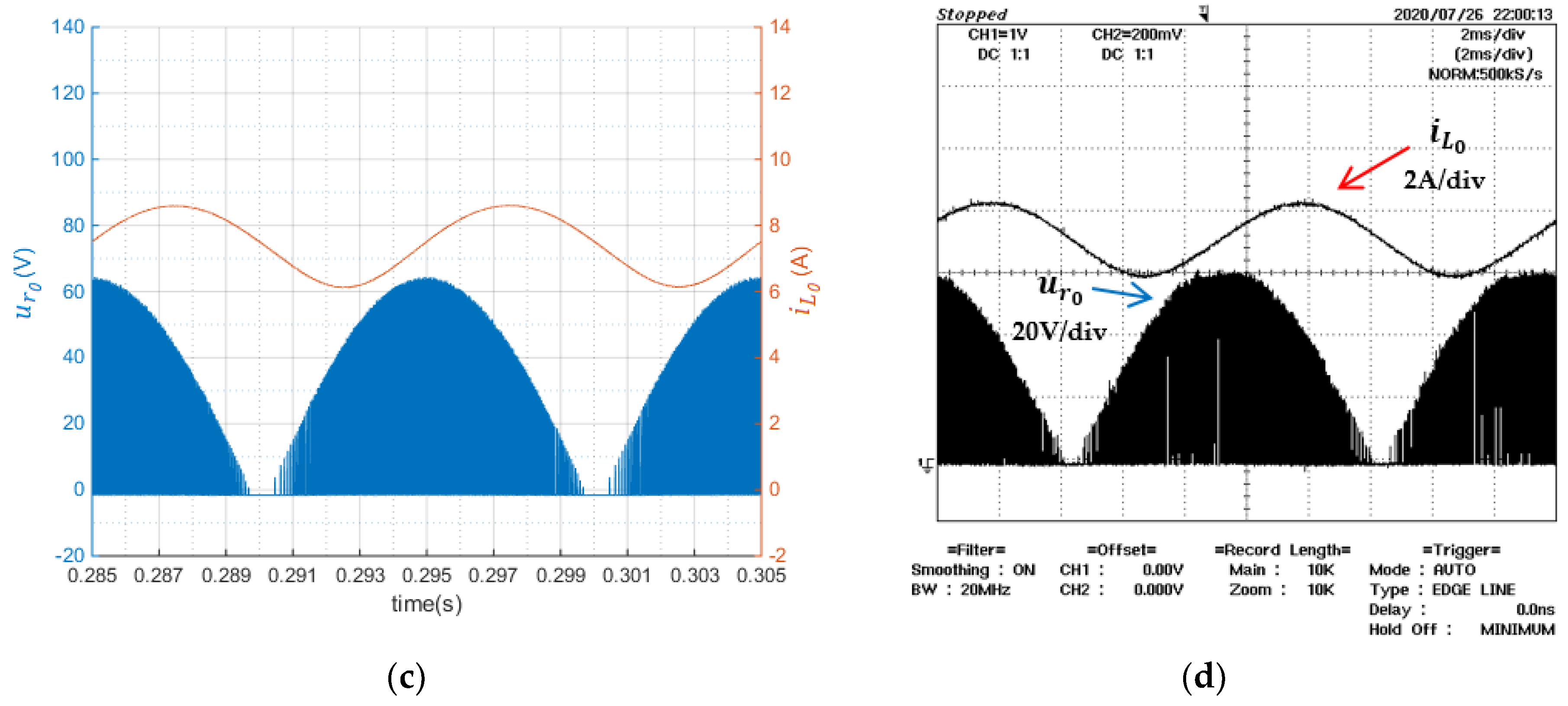
In Figure 11c, the simulation results of the high-frequency rectified voltage u r 0 with 63 Vpeak and current i L 0 are presented to be comparable with the experimental results in Figure 11d with voltage u r 0 with 60 Vpeak.
Figure 12a shows the direct current i L 0 of the simulation with significant oscillation of 2.5 A around the average value reference i L 0 r e f of 7.5 A, similar to the experimental results presented in Figure 12b, with 2.4 and 7.5 A, respectively. Figure 12c shows the waveforms’ voltage u 0 with 24 V and current i 0 with 5 A for simulation, while in the experimental results (Figure 12d), the same voltage and current values were obtained. The difference between these two results’ waveforms is in the ripple value of the voltage, which in the simulation case presents about Δ u 0 = 0.6 V and for the experimental case present around Δ u 0 = 1.2 V. The experimental results have an extra delay time due to the voltage u 0 measuring circuits. This delay time was not considered in the simulation. The output voltage remains constant throughout the one cycle of the AC network.

5. Conclusions

This paper presented the design of digital controllers for a single-phase AC-DC converter, including a high-frequency isolation transformer and low-value non-electrolytic capacitors, to be introduced into a future low-voltage DC network for residential buildings, as an alternative to traditional AC power networks. Control using sliding mode (for binary variables) and the Lyapunov direct method of stability (for sampled quantities), together with separation of fast and slow dynamics, were shown as viable choices for the digital control of a fourth order dynamics isolated AC-DC converter. The designed controllers were able to guarantee the stability and the robustness of the sliding mode controllers ensured almost zero error tracking of the output voltage, while ensuring near unity power factor operation. This unidirectional converter can be applied to a residential low-DC voltage network without energy generation with the benefit of avoiding current stresses in the low-value non-electrolytic output capacitors of the DC bus, which is achieved using the described control techniques. The converter can be used in DC buses with energy storage, where it can increase the battery lifetime, by reducing the charging current ripple. The analysis of the results shows the converter has fast enough response times (disturbances smaller than the switching ripple), even in situations of greater dynamic load demand, tested for abrupt variations of 25% of the nominal power with a minimum impact in the AC network, since the unity power factor operation is guaranteed in transient operation.
The digital implementation in a dual CPU DSP was programmed via Matlab/Simulink, with the explicit usage of each Core for a specific control task. The low-cost TI CPU selected has a good development tool for a fast prototyping control system needed in high-frequency power electronic converters.

Author Contributions

N.S. designed and performed the experiments, analyzed the data and wrote the manuscript. J.F.S. supervised the research, providing guidance theory, analyzed the data and wrote the paper. V.S. supervised, performed the experiments and provided key suggestions. All authors have read and agreed to the published version of the manuscript.

Funding

This work was supported by national funds through FCT, Fundação para a Ciência e a Tecnologia, under project UIDB/50021/2020.

Conflicts of Interest

The authors declare no conflict of interest.

References

  1. Marzband, M.; Ardeshiri, R.R.; Moafi, M.; Uppal, H. Distributed generation for economic benefit maximization through coalition formation-based on Game Theory. Int. Trans. Electr. Energy Syst. 2017, 27, e2313. [Google Scholar] [CrossRef]
  2. Walter, D.; Mariacristina, R.; Dario, Z. Hybrid photovoltaic system control for enhancing sustainable energy. In Proceedings of the IEEE Power Engineering Society Summer Meeting, Chicago, IL, USA, 21–25 July 2002; Volume 1, pp. 134–139. [Google Scholar]
  3. Han, Y.; Chen, W.; Li, Q. Energy Management Strategy Based on Multiple Operating States for a Photovoltaic/Full Cell/Energy Storage DC Microgrid. Energies 2017, 10, 136. [Google Scholar] [CrossRef] [Green Version]
  4. Gerber, D.L.; Vossos, V.; Feng, W.; Khandekar, A.; Marnay, C.; Nordman, B. A simulation based comparison of AC and DC power distribution networks in buildings. In Proceedings of the IEEE Second International Conference on DC Microgrids (ICDCM), Nuremburg, Germany, 27–29 June 2017; pp. 588–595. [Google Scholar]
  5. Chauhan, R.K.; Rajpurohit, B.S.; Hebner, R.E.; Singh, S.N.; Gonzalez-Longatt, F.M. Voltage Standardization of DC Distribution System for Residential Buildings. J. Clean Energy Technol. 2015, 4, 167–172. [Google Scholar] [CrossRef]
  6. Li, W.; Mou, X.; Zhou, Y.; Marnay, C. On voltage standards for DC home microgrids energized by distributed sources. In Proceedings of the 7th International Power Electronics and Motion Control Conference (IPEMC), Harbin, China, 2–5 June 2012; Volume 3, pp. 2282–2286. [Google Scholar]
  7. Arunkumar, G.; Devaraj, E.; Padmanaban, S.; Hossain, E.; Leonowicz, Z.; Joseph, P.K. DC Grid for Domestic Electrification. Energies 2019, 12, 2157. [Google Scholar] [CrossRef] [Green Version]
  8. Pratt, A.; Kumar, P.; Aldridge, T.V. Evaluation of 400V DC distribution in telco and data centers to improve energy efficiency. In Proceedings of the INTELEC 29th International Telecommunications Energy Conference, Rome, Italy, 30 September–4 October 2007; pp. 32–39. [Google Scholar]
  9. Public Overview of the Emerge Alliance Data/Telecom Center Standard; EMerge Alliance: San Ramon, CA, USA, 2012; Available online: http://www.directpowertech.com/docs/PublicOverviewoftheEMergeAllianceDataTelecom_21298_2.pdf (accessed on 31 July 2020).
  10. Priyadharshini, G.; Nandhini, N.R.; Shunmugapriya, S.; Ramaprabha, R. Design and simulation of smart sockets for domestic DC distribution. In Proceedings of the International Conference on Power and Embedded Drive Control (ICPEDC), Chennai, India, 16–18 March 2017; pp. 426–429. [Google Scholar]
  11. Shivakumar, A.; Normark, B.; Welsch, M. Household DC Networks: State of the Art and Future Prospects; Insight_E. 2015. Available online: https://www.sun-connect-news.org/fileadmin/DATEIEN/Dateien/New/DCnetworks_Final.pdf (accessed on 31 July 2020).
  12. López-Santos, O.; Cabeza-Cabeza, A.J.; García, G.; Martínez-Salamero, L. Sliding Mode Control of the Isolated Bridgeless SEPIC High Power Factor Rectifier Interfacing an AC Source with a LVDC Distribution Bus. Energies 2019, 12, 3463. [Google Scholar] [CrossRef] [Green Version]
  13. Lin, X.; Wang, F.; Iu, H.H.C. A New Bridgeless High Step-up Voltage Gain PFC Converter with Reduced Conduction Losses and Low Voltage Stress. Energies 2018, 11, 2640. [Google Scholar] [CrossRef] [Green Version]
  14. Singh, B.; Chandra, A.; Al-Haddad, K.; Pandey, A.; Kothari, D.P. A review of single-phase improved power quality ac~dc converters. IEEE Trans. Ind. Electron. 2003, 50, 962–981. [Google Scholar] [CrossRef] [Green Version]
  15. Reimensnyder, N.; Weise, N. Voltage control of a single phase, single-stage, isolated AC-DC converter. In Proceedings of the 2013 IEEE Transportation Electrification Conference and Expo (ITEC), Detroit, MI, USA, 16–19 June 2013; pp. 1–5. [Google Scholar]
  16. Agarwal, T.; Bhardwaj, S.K.; Katara, K.K.; Pareta, R. A Review and Comparative Study on Single-Phase Ac-Dc Converters for Their High Frequency Applications. In Proceedings of the International Conference Proceeding ICCCT, Allahabad, India, 24–26 November 2017; Available online: http://www.ijcrt.org/papers/IJCRTICCC002.pdf (accessed on 31 July 2020).
  17. Lin, B.; Hwang, T. Single phase rectifier with high power factor in continuous and discontinuous conduction mode. In Proceedings of the IEEE International Symposium on Industrial Electronics, Dubrovnik, Croatia, 10–14 July 1995; Volume 1, pp. 421–426. [Google Scholar]
  18. Vossos, E. Optimizing Energy Savings from “Direct-DC” in US Residential Buildings; Ernest Orlando Lawrence Berkeley National Laboratory: Berkeley, CA, USA, 2011. [Google Scholar]
  19. Vossos, V.; Garbesi, K.; Shen, H. Energy savings from direct-DC in U.S. residential buildings. Energy Build. 2014, 68, 223–231. [Google Scholar] [CrossRef]
  20. Savage, P.; Nordhaus, R.R.; Jamieson, S.P. Dc Microgrids: Benefits and Barriers. In From Silos to Systems: Issues in Clean Energy and Climate Change; Yale School of Forestry & Environmental Studies: New Haven, CT, USA, 2010; pp. 51–66. [Google Scholar]
  21. Rodriguez-Otero, M.A.; O’Neill-Carrillo, E. Efficient Home Appliances for a Future DC Residence. In Proceedings of the 2008 Energy 2030 Conference, Atlanta, Georgia, 17–18 November 2008; Volume 6, pp. 17–18. [Google Scholar]
  22. Costa, P.B.; Silva, J.F.; Pinto, S.F. Experimental evaluation of SiC MOSFET and GaN HEMT losses in inverter operation. In Proceedings of the IEEE IECON 2019-45th Annual Conference of the IEEE Industrial Electronics Society, Lisbon, Portugal, 14–17 October 2019; pp. 6595–6600. [Google Scholar]
  23. Watanabe, H.; Itoh, J.-I.; Koike, N.; Nagai, S. PV Micro-Inverter Topology Using LLC Resonant Converter. Energies 2019, 12, 3106. [Google Scholar] [CrossRef] [Green Version]
  24. Santos, N.; Silva, J.F.; Soares, V. High-Frequency Transformer Isolated AC-DC Converter for Resilient Low Voltage DC Residential Grids. In Technological Innovation for Resilient Systems; Springer: Cham, Switzerland, 2018; pp. 147–155. [Google Scholar]
  25. Zhang, H.; Li, X.; Ge, B.; Balog, R.S. Capacitance, dc Voltage Utilizaton, and Current Stress: Comparison of Double-Line Frequency Ripple Power Decoupling for Single-Phase Systems. IEEE Ind. Electron. Mag. 2017, 11, 37–49. [Google Scholar] [CrossRef]
  26. Singh, B.P.; Singh, S.; Chandra, A.; Al-Haddad, K. Comprehensive Study of Single-Phase AC-DC Power Factor Corrected Converters with High-Frequency Isolation. IEEE Trans. Ind. Inform. 2011, 7, 540–556. [Google Scholar] [CrossRef]
  27. Shamshuddin, M.A.; Rojas, F.; Cárdenas, R.; Pereda, J.; Diaz, M.; Kennel, R. Solid State Transformers: Concepts, Classification, and Control. Energies 2020, 13, 2319. [Google Scholar] [CrossRef]
  28. Licea, M.A.R.; Pinal, F.J.P.; Perez, J.C.N.; Herrera, C. Nonlinear Robust Control for Low Voltage Direct-Current Residential Microgrids with Constant Power Loads. Energies 2018, 11, 1130. [Google Scholar] [CrossRef] [Green Version]
  29. Paraíso, G.M.; Silva, J.F.; Pinto, S.F. Control strategies for low voltage DC residencial grids with constant power loads. In 2018 International Young Engineers Forum (YEF-ECE); IEEE: New York, NY, USA, 2018; pp. 67–72. [Google Scholar]
  30. Silva, J.F.; Pinto, S.F. Linear and Nonlinear Control of Switching Power Converters. In Power Electronics Handbook, 4th ed.; Butterworth-Heinemann: Oxford, UK, 2017; pp. 1141–1220. [Google Scholar]
  31. Silva, J.F. Sliding Mode Control of Voltage Sourced Boost-Type Reversible Rectifiers. In Proceedings of the IEEE/ISIE’97 Conference, Guimarães, Portugal, 7–11 July 1997; IEEE: New York, NY, USA, 1997; Volume 2, pp. 329–334. [Google Scholar]
  32. Martins, J.F.; Pires, A.J.; Silva, F.A. A novel and simple current controller for three-phase PWM power inverters. IEEE Trans. Ind. Electron. Spec. Sect. PWM Curr. Regul. 1998, 45, 802–805. [Google Scholar] [CrossRef]
  33. Santos, N.; Silva, F.A.; Santana, J. Sliding Mode Control of Unified Power Quality Conditioner for 3 Phase 4 Wire Systems. In Doctoral Conference on Computing, Electrical and Industrial Systems; Springer: Berlin/Heidelberg, Germany, 2014; pp. 443–450. [Google Scholar]
  34. Yasin, A.R.; Ashraf, M.; Bhatti, A.I. Fixed Frequency Sliding Mode Control of Power Converters for Improved Dynamic Response in DC Micro-Grids. Energies 2018, 11, 2799. [Google Scholar] [CrossRef] [Green Version]
  35. Serna, S.; González-Montoya, D.; Ramos-Paja, C.A. Control of a Charger/Discharger DC/DC Converter with Improved Disturbance Rejection for Bus Regulation. Energies 2018, 11, 594. [Google Scholar] [CrossRef] [Green Version]
  36. Tan, Y.; Chang, J.; Tan, H. Advanced Motion Control Scheme with Integrator backstepping: Design and Analysis. In Proceedings of the 2000 IEEE 31st Annual Power Electronics Specialists Conference, Galway, Ireland, 23–23 June 2000. [Google Scholar]
  37. Escudero, M.; Kutschak, M.-A.; Meneses, D.; Rodriguez, N.; Morales, D.P. A Practical Approach to the Design of a Highly Efficient PSFB DC-DC Converter for Server Applications. Energies 2019, 12, 3723. [Google Scholar] [CrossRef] [Green Version]
  38. Pindoriya, R.M.; Pindoriya, N.M.; Rajendran, S. Simulation of DC/DC converter for DC nano-grid integrated with solar PV generation. In 2015 IEEE Innovative Smart Grid Technologies—Asia (ISGT ASIA); IEEE: New York, NY, USA, 2015; pp. 1–6. [Google Scholar]
  39. Rigogiannis, N.; Voglitsis, D.; Jappe, T.; Papanikolaou, N. Voltage Transients Mitigation in the DC Distribution Network of More/All Electric Aircrafts. Energies 2020, 13, 4123. [Google Scholar] [CrossRef]
  40. Kim, M.; Lee, S.G.; Bae, S. Decentralized Power Management for Electrical Power Systems in More Electric Aircrafts. Electronics 2018, 7, 187. [Google Scholar] [CrossRef] [Green Version]
Figure 1. Proposed isolated AC-DC for DC low-voltage residential networks.
Electronics 09 01401 g001
Figure 2. Simplified control block diagram proposed for the isolated AC-DC converter.
Electronics 09 01401 g002
Figure 3. Simulation waveforms: (a) primary side, the variables are u S , u C 1 , u T 1 and i L s ; (b) secondary side, the variables are u r o , u 0 , i L 0 r e f , i L 0 and i 0 .
Electronics 09 01401 g003
Figure 4. Simulation waveforms for different voltage references: (a) u 0 r e f = 12 V; (b) u 0 r e f = 28 V.
Electronics 09 01401 g004
Figure 5. Simulation waveforms for variation in amplitude of AC main voltage.
Electronics 09 01401 g005
Figure 6. Time evolution in transient conditions.
Electronics 09 01401 g006
Figure 7. Experimental prototype workbench: (a) the main primary side; (b) secondary side.
Electronics 09 01401 g007
Figure 8. TI DSP Core 1 digital control block diagram for the u C 1 voltage control.
Electronics 09 01401 g008
Figure 9. Core 2 digital control block diagram of TI DSP: (a) current reference i L 0 r e f ; (b) current controller i L 0 ; (c) current controller i L s ; (d) global diagram blocks implemented in Core 2.
Electronics 09 01401 g009
Figure 10. Waveforms at primary side of the AC-DC converter: (a) simulation results of voltage u s and current i L S ; (b) experimental results of voltage u s and current i L S ; (c) simulation results of voltage u C 1 ; (d) experimental results of voltage u C 1 ; (e) simulation results of voltage u T 1 and current i L S ; (f) experimental results of voltage u T 1 and current i L S .
Electronics 09 01401 g010aElectronics 09 01401 g010b
Figure 11. Waveforms in the AC-DC converter: (a) simulation results of voltage u T 1 and current i T 1 ; (b) experimental results of voltage u T 1 and current i T 1 ; (c) simulation results of voltage u r 0 and current i L 0 ; (d) experimental results of voltage u r 0 and current i L 0 .
Electronics 09 01401 g011aElectronics 09 01401 g011b
Figure 12. Waveform at output side of the AC-DC converter: (a) simulation results of current i L 0 and current i 0 ; (b) experimental results of current i L 0 and current i 0 ; (c) simulation results of voltage u 0 and current i 0 ; (d) simulation results of voltage u 0 and current i 0 .
Electronics 09 01401 g012aElectronics 09 01401 g012b
Table 1. Parameters inherent to the AC-DC converter to validate the proposed model.
SymbolDescriptionValueSymbolDescriptionValue
u S AC peak voltage110 V Δ u C 1 Ripple   of   u C 1 4 V
f S AC frequency50 Hz Δ i L s Ripple   of   i L s 0.1 A
u 0 DC voltage24 V Δ u 0 Ripple   of   u 0 0.4 V
P 0 Power of load120 W Δ i L 0 Ripple   of   i L 0 3 A
  η Proposed efficiency90 %nTransformer ratio1.6
L s Input inductor1.2 mH L 0 Output inductor 25 mH
C 1 Input capacitor8 µF C 0 DC-bus capacitor200 µF