Article

Evaluation Method of Heavy-Ion-Induced Single-Event Upset in 3D-Stacked SRAMs

1
Institute of Modern Physics, Chinese Academy of Sciences, Lanzhou 730000, China
2
School of Nuclear Science and Technology, University of Chinese Academy of Science, Beijing 100049, China
*
Author to whom correspondence should be addressed.
Electronics 2020, 9(8), 1230; https://doi.org/10.3390/electronics9081230
Submission received: 8 June 2020 / Revised: 23 July 2020 / Accepted: 28 July 2020 / Published: 30 July 2020
(This article belongs to the Special Issue Extreme-Environment Electronics: Challenges and Solutions)

Abstract

:
The interaction of radiation with three-dimensional (3D) electronic devices can be determined through the detection of single-event effects (SEU). In this study, we propose a method for the evaluation of SEUs in 3D static random-access memories (SRAMs) induced by heavy-ion irradiation. The cross-sections (CSs) of different tiers, as a function of the linear energy transfer (LET) under high, medium, and low energy heavy-ion irradiation, were obtained through Monte Carlo simulations. The simulation results revealed that the maximum value of the CS was obtained under the medium-energy heavy-ion penetration, and the effect of penetration range of heavy ions was observed in different tiers of 3D-stacked devices. The underlying physical mechanisms of charge collection under different heavy-ion energies were discussed. Thereafter, we proposed an equation of the critical heavy-ion range that can be used to obtain the worst CS curve was proposed. Considering both the LET spectra and flux of galactic cosmic ray (GCR) and the variation in the heavy-ion Bragg peak values with the atomic number, we proposed a heavy-ion irradiation test guidance for 3D-stacked devices. In addition, the effectiveness of this method was verified through simulations of the three-tier vertically stacked SRAM and the ultrahigh-energy heavy-ion irradiation experiment of the two-tier vertically stacked SRAM. this study provides a theoretical framework for the detection of SEUs induced by heavy-ion irradiation in 3D-integrated devices.

1. Introduction

As gate-length scaling pushes the development of high-density integrated circuits (ICs) from large-scale integrations to ultra-large-scale integrations, various concerns such as high off-state and sub-threshold leakage, along with substantial delays in wiring, are becoming more serious. Thus, it is difficult to obtain high performance through improved integration by scaling the feature size of a transistor. To increase both performance and functionality of ICs and to reduce power and cost, three-dimensional (3D) IC packaging technology emerged as a potential solution [1,2,3]. This 3D IC integration allows multiple two-dimensional (2D) circuits to be stacked vertically as a single die, with improved integration density, noise immunity, superior performance, and higher reliability. Hence, 3D IC technology is a promising candidate for aerospace applications.
When high-energy particles are incident on the sensitive area of the device, they deposit energy and generate a high number of electron–hole pairs through ionization. If the ionized charge is collected by the sensitive node, a transient current pulse occurs, which changes the logic state of the latch (single-event upset (SEU)). In recent years, scientists conducted a series of studies on the impact of high-energy heavy ions on 3D devices. The total ionizing dose (TID) effects in 150-nm silicon on insulator (SOI) and 130-nm bulk silicon 3D vertically stacked technology devices were studied by Gouker et al. [4] and Re et al. [5], respectively. The results demonstrated that the 3D device TID tolerance is similar to or better than its corresponding counterparts in a standard 2D device. In addition, novel radiation damage induced by the mechanical and thermal stresses occurring during the fabrication of the 3D integrated IC was not observed. In particular, Gouker et al. observed that the upper tiers in SOI technology stacking circuits have better TID-tolerant performance than the lower tiers [4] caused by the change in electric field distribution and strength in the buried oxide (BOX) when the silicon substrate is removed, resulting in a decrease in the density of the positive charge trapped in the BOX. Although the study of Zeng et al. indicated that the leakage current of through-silicon via (TSV) metal–oxide–semiconductor (MOS) structure would increase after exposure to gamma ray irradiation [6], it is important and necessary to consider the effect of radiation on the reliability of TSV-based applications under radiation conditions. Moreover, the single-event effects (SEE) in the 150-nm SOI and bulk silicon 3D static random-access memory (SRAM) circuits were evaluated by Gouker et al. (proton, neutron, and heavy ion) [7,8] and Uznanski et al. (proton) [9]. The experimental results indicated that the radiation effects on 2D and 3D SRAMs fabricated using the same techniques have a similar response, but high-Z materials such as tungsten can have an impact on the SEE sensitivity of the lower tiers. Owing to the back metal layer available on the upper tiers in the SOI complementary metal–oxide–semiconductor (CMOS) tier stacked circuit, it can be used as a back gate to tune the field-effect transistor (FET) current drive and attenuate the Single-event transient (SET) pulse width and cross-section (CS) [8]. Furthermore, the impacts of the various energies of proton and heavy-ion irradiation on the 90-nm and 55-nm 3D bulk silicon IC technology were also evaluated by Gupta et al. [10] and Cao et al. [11]. The results showed that the SEU CSs of 3D SRAMs were significantly dependent on the energy of incoming particles, and that the discrepancy between each tier CS could reach several orders of magnitude in the ascending regions. Meanwhile, the percentage of multiple cell upsets also exhibited differences in the saturated regions.
Linear energy transfer (LET) is the average amount of energy that an ionizing particle transfers to the material traversed per unit distance. According to the theory of interactions between heavy ions and matter, with the decrease in energy, the LET value of ions gradually increases and thereafter decreases rapidly. Standard guides for measuring SEU in conventional 2D ICs from heavy-ion irradiation require that the range of the ions be at least 30 μm in silicon to ensure the ions have sufficient penetration to reach the sensitive volume [12,13]. However, the 30-μm penetration depth of the ions did not ensure that the ions could pass through all sensitive volumes in the several-hundred-micrometer-thick vertically stacked 3D ICs. Meanwhile, the heavy-ion LET significantly changes as the ions travel through hundreds of micrometers of stacked material. Therefore, using heavy-ion LET to characterize the radiation effects on the 3D ICs poses a significant challenge. In this study, we construct a three-tier stacked hypothetical SRAM based on the technique information extracted through reverse engineering and the corresponding heavy-ion radiation experimental data. Each tier’s SEU CSs of heavy ions with various species, energies, and LETs were studied through Monte Carlo simulation. Considering the crucial requirements of the high-security marginal design of electronic devices for aerospace engineering, the test procedures for the evaluation of SEEs in 3D ICs induced by heavy-ion irradiation were proposed. Our study provides theoretical guidance for the measurement of single-event effects, which are induced through heavy-ion irradiation of 3D-stacked ICs or those devices with a thick substrate above the sensitive volume region.

2. Experimental and Monte Carlo Simulation Details

2.1. Devices under Test (DUT) and Heavy-Ion Experimental Data

The devices evaluated in this study were 180-nm radiation-hardened bulk silicon SRAM and two types of 130-nm SOI process SRAMs. The rectangular parallelepiped (RPP) model of 180-nm bulk silicon SRAM was obtained from previously published articles [14,15,16], and the corresponding SEU thresholds and saturation SEU CSs were 30 MeV·cm2/mg and 4 × 10⁻⁸ cm2/bit, respectively. Moreover, the SV and RPP geometry for this planar bulk silicon SRAM were 2 μm × 2 μm × 2.25 μm and 5 μm × 5 μm × 30 μm, respectively. Two types of unit circuits of 6T and active delay element (ADE) radiation-hardened SRAMs were manufactured through partially depleted SOI (PDSOI) process technology in one wafer. The passivation and metal layers were approximately 7.0 μm thick, and the unit cell for this planar PDSOI SRAM was 3 μm × 3 μm.
To determine the sensitive size of SOI SRAMs, heavy-ion irradiation testing was performed on the cyclotron of the Heavy Ion Research Facility in Lanzhou (HIRFL). The SEU CS as a function of the LET is illustrated in Figure 1 (solid black triangle). The SEU threshold LETs of 6T SRAM and ADE SRAM were 4 MeV·cm2/mg and 35 MeV·cm2/mg, respectively. We assume that the length multiplied by the width of the sensitive region (RPP model) is equal to the saturated CS value (L × W = σsat) The length and width of the sensitive region were obtained from the square root of σsat (L = W = σ sat ). The height of the sensitive region of an SOI SRAM device is the thickness of the silicon film (260 nm). Because the saturated SEU CSs of 6T SRAM and ADE SRAM were 2 × 10⁻⁸ cm2/bit and 9 × 10⁻⁸ cm2/bit, respectively, we could set the corresponding SVs as 1.4 μm × 1.4 μm × 0.26 μm and 0.3 μm × 0.3 μm × 0.26 μm, respectively.
The direct ionization and the nuclear reaction physical modes were both considered in numerical simulations using the CRÈME-MC toolkit [17,18,19]. To obtain better statistical data, 100,000 heavy ions were irradiated at each experimental data point. As illustrated in Figure 1, the solid blue circles reflect the simulation results with the same parameters used in the heavy-ion radiation experiment. Thus, the simulation results correspond with the experimental data, indicating that the SV geometries of SOI SRAMs and the corresponding physical mode used in numerical computation are credible and valid.

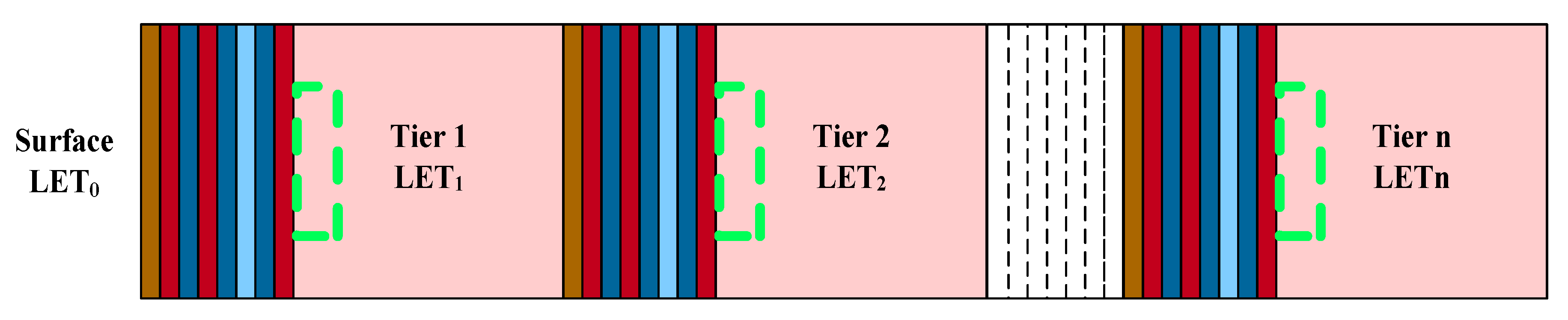
2.2. 3D Models of Bulk Silicon and SOI SRAM and the Numerical Simulation Details

In our study, the 3D device model for Monte Carlo simulation was a three-tier stacked structure, and the total thickness was 90 μm (each tier was 30 μm), as described in Figure 2. Based on the total thickness of the 3D-stacked RPP models, high, medium, and low energy were selected for investigating the different tier SEU sensitivities. Firstly, high energy was defined as the corresponding heavy-ion range that is significantly larger than the total thickness of 3D devices (Rions >> T3D) Thus, the LET is almost constant at each tier’s SV during heavy-ion penetration through the 3D device. Secondly, medium energy was defined as the range of heavy ion that is comparable to the thickness of the 3D device (Rions ≈ T3D). Thus, the change in LET value for heavy-ion penetration through different sensitive tiers increases with the increment of the corresponding atomic number. Finally, low energy was defined as the corresponding heavy-ion range that is less than the total thickness of 3D devices (Rions < T3D). Some lower-tier SVs cannot be penetrated by heavy ions. The range of heavy ions with different energies was calculated using SRIM-2013 [20].

3. Monte Carlo Simulation of 3D-Stacked Structure Devices

3.1. Results and Discussion of Monte Carlo Simulation for 3D-Stacked SRAMs

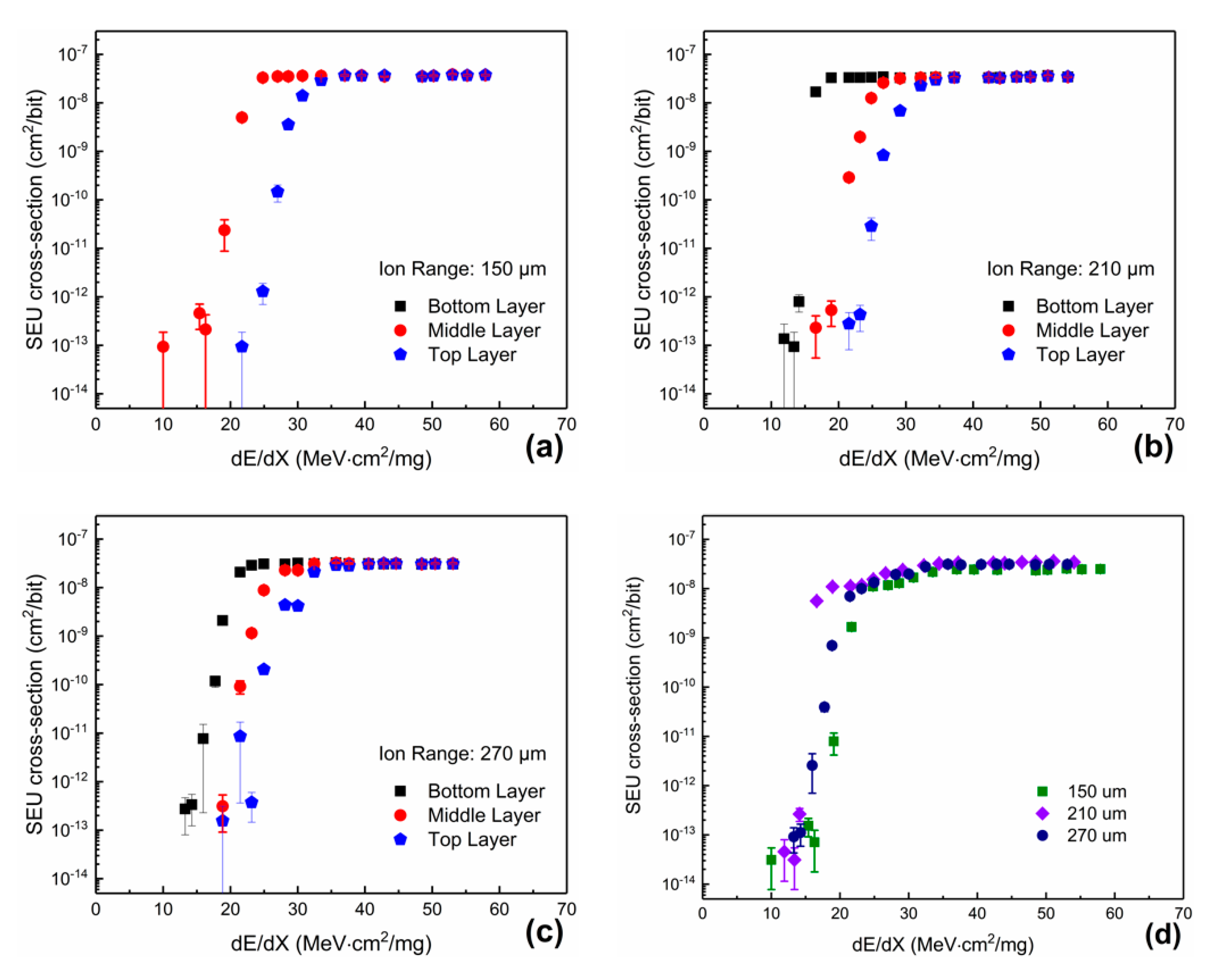
3.1.1. Simulation Results of Each Tier’s CS under Different Heavy-Ion Energy Conditions

As described in Figure 3a–c, when high-energy heavy ions are incident on 3D-stacked devices, the SEU CSs of the top, middle, and bottom tiers are almost similar. Comparing the simulation results of the three-tier models, we can conclude that the value of threshold LET is directly proportional to the ascending region occupied in the CS curve. Therefore, the high-energy heavy ion is suggested when investigating the radiation failure mechanism for 3D-stacked devices.
Figure 3d–f illustrates the simulation results for the heavy ions with 90-μm range penetrating the 3D-stacked devices. The change in LET value in the three-tier SV cannot be neglected when the medium-energy heavy ions penetrate the 3D RPP models. Notably, the CS value is nearly equal for each tier in the saturated region, even when the LET values are different in the top, middle, and bottom tiers. Meanwhile, the CS value exhibits a significant discrepancy between the three tiers in the ascending region. Comparing the simulation results of the bulk silicon model (Figure 3d) and the ADE SOI model (Figure 3f), when their SEU thresholds are similar, we can conclude that a bigger SV leads to a clearer discrepancy of the CS in the ascending region. Comparing the results of the 6T SOI model (Figure 3e) and the ADE SOI model (Figure 3d), we can observe that a higher threshold LET accompanies the larger relative discrepancy of the CS in the ascending region.
As shown in Figure 3g–i, the CS value of the bottom tier is close to zero because the low-energy heavy ions with a 60-μm range cannot penetrate to the bottom tier. Therefore, low-energy heavy ions are not recommended in radiation experiments when investigating the single-event effect sensitivity of 3D-stacked devices. Notably, in the saturated region, the CS values of the top and the middle tiers for low-energy conditions correspond with the medium-energy heavy ions. Meanwhile, in the ascending region, the CS discrepancy increases further between the top tier and the middle tier compared with the medium-energy heavy-ion conditions.

3.1.2. Numerical Results Comparing the CS Per Bit under Different Heavy-Ion Energies

As depicted in Figure 4, the CS values per bit were obtained under different heavy-ion energy penetration conditions. In the saturated SEU CS region of the three stacked models, the maximum value of the CS per bit was obtained under medium-energy heavy-ion striking. Moreover, the discrepancy between SEU CS per bit under different heavy-ion energies becomes more significant when the threshold LET increases or the sensitive volume decreases. The underlying physical mechanism of this CS discrepancy can be explained as follows: the density of electron–hole pairs around the heavy-ion track core decreases with the energy increase; then, the lower CS per bit is obtained under relatively higher-energy heavy-ion conditions. Notably, the SEU CS per bit obtained under low energy conditions is as high as for the high-energy condition because the top and middle tier CSs enlarge to 1.5 times or more under low-energy conditions.
In the ascending region, there is an obvious discrepancy of average CS when heavy ions with different energy penetrate the stacked devices. The discrepancy is mainly caused by the fact that the LET value increases as the heavy-ion energy decreases when the heavy ions penetrate the same depth in silicon. Therefore, the bottom tier’s sensitive layers deposit additional energy under the relatively low-energy heavy-ion conditions. Thus, the concept of LET must be carefully used in radiation testing and simulation computation when the SV is relatively small.

3.2. Critical Range of Heavy Ions to Evaluate SEE CS of 3D Devices

When the area enclosed by the CS curve and the abscissa is larger than other conditions, we refer to it as the worst curve. To obtain the worst curve of the SEU CS, the LETs in each tier’s sensitive layer must not be less than the surface LET. When the penetrating depth of heavy ions increases in the stacked devices, the heavy-ion LET gradually increases to the Bragg peak and thereafter dramatically decreases to zero. Therefore, the heavy-ion range should meet one of the following conditions:
{ L 0 L 1 , L 2 , , L n L 0 L th L 0 L 1 L 2 L n L 0 L th ,
where L0, L1, …, Ln represent LET0, LET1, …, LETn, as described in Figure 5. Lth denotes the threshold LET of the SEU, and we assume that the threshold LETs are similar for each tier. Based on the simulation results and the corresponding conclusions mentioned above, we propose the critical range equation for heavy-ion irradiation testing to get the maximum CS value for the vertically stacked devices as follows:
R th = ( n 1 ) × T 2 D + R BP + T P + T S ,
where Rth represents the critical range of heavy ions, n is the total number of the stacked tiers, and T2D is the thickness of a single tier. When the heavy-ion Bragg peak LET is equal to the threshold LET, the corresponding range is RBP. TP denotes the thickness of overlays above the SV. TS is the thickness of SV. Therefore, all heavy-ion ranges used in radiation experiments must not be less than the minimum range determined from Equation (2).
Following this critical range condition, we can ensure that the LETs in each tier’s sensitive layer are not less than the surface LET before the surface LET reaches the saturated LET; subsequently, we can obtain the maximum curve of the CS. Substituting the parameters of the stacked structure of bulk silicon SRAM, 6T SOI SRAM, and ADE SOI SRAM models into the critical range equation, we obtain Rth ≈ 90 μm, which is consistent with the simulation results. To further verify the effectiveness of this equation, the single-tier thickness of bulk silicon SRAM was modified from 30 μm (Rth ≈ 90 μm) to 90 μm (Rth ≈ 210 μm). The simulation results are presented in Figure 6. Three ion ranges (150 μm, 210 μm, and 270 μm) were selected for calculating the corresponding CS values. The worst curve of CS was obtained when the heavy-ion range was 210 μm. The equation provides excellent prediction capabilities to guide the ground heavy-ion irradiation experiments of these 3D vertically stacked devices.

4. On-Orbit SEU Rate Prediction Methodology Based on Accelerator Test Experimental Data

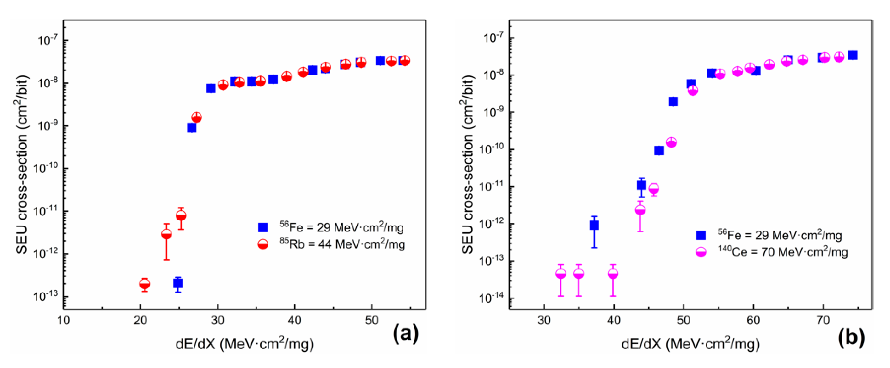
4.1. Discussion of the SEE Test Standards of 3D Vertically Stacked Device

For the ground-level heavy-ion radiation testing, the worst experimental conditions should be used to obtain the most conservative radiation results, such that we can screen out the maximum safety margin electronic devices. From Equation (2), we can compute the critical heavy-ion range of various threshold LETs; however, different threshold LETs accompany different critical, heavy-ion ranges. Thus, Equation (2) is not appropriate for testing standard guidelines. Therefore, the crucial question for SEE testing standard is to select the lowest calibration ions, covering the maximum range of threshold LETs.
To determine the critical calibration heavy ions, the integral LET spectrum of GEO Orbit was computed using CRÈME-MC simulator, as shown in Figure 7a. The ordinate value of Figure 7a provides the flux value of particles that have LET greater than the corresponding abscissa value. There is a cliff descent of approximately 29 MeV·cm2/mg, caused by the relative abundance spectrum of the galactic cosmic ray (GCR) ions. The relative abundance spectrum has a steep drop-off when the atomic number is higher than that of iron [21]. We calculated the heavy-ion Bragg peak value using SRAM-2013, as shown in Figure 7b, and we can conclude that the relationship between the Bragg peak LET of heavy ions (the left ordinate) and the corresponding atomic number (the abscissa) from helium (Z = 2) to uranium (Z = 92) is linear. Meanwhile, the relationship between the Bragg peak range of heavy ions (the right ordinate) and the corresponding atomic number (the abscissa value) is not linear. There is a platform region of Bragg peak ranges near the iron ions (the change in ranges from 22 μm to 26 μm corresponding to the change in LETs from 29 MeV·cm2/mg to 46 MeV·cm2/mg).
Thus, the iron ion was selected as the calibration ion to determine the critical heavy-ion range used in the irradiation experiment and simulation for 3D vertically stacked devices. Equation (2) can be rewritten as follows:
R th = ( n 1 ) × T 2 D + R Fe BP + T p + T S
The range of the 56Fe Bragg peak is 22 μm; thus, the lowest SV abscissa value of the 3D vertically stacked device is 22 μm, as depicted in Figure 8. The corresponding heavy-ion species are 74Ge, 102Ru, and 208Pb, with LETs equivalent to 37 MeV·cm2/mg, 49 MeV·cm2/mg, and 75 MeV·cm2/mg at the 22-μm range (blue line).
As illustrated in Figure 8, compared with Ln, from 4He to 238U, the surface LET has three stages. For example, if the total thickness of the 3D-stacked device is 44 μm, the corresponding abscissa values are 66 μm (L0–2) to 22 μm (Ln) in Figure 8. We observe that the comparison between L0–2 and Ln has three changes, from L0–2 < Ln (z < 44) to L0–2 = Ln (z = 44) and then to L0–2 > Ln (z > 44). Therefore, the worst radiation condition in Equation (1) can be rewritten as follows:
{ L 0 < L n L 0 = L n L 0 , L n > L th Before   L 0 = L n L th When   L 0 = L n L th After   L 0 = L n L th
The total thickness of the 3D vertically stacked device must satisfy the conditions described in Equation (4). When the SEU threshold LET value is 49 MeV·cm2/mg, the heavy ions whose LET value is equal to this threshold in the blue line are 102Ru ions; the same LET value at the left side of the Bragg peak for 102Ru ions is 66 μm, as described in Figure 8. If the thickness (from surface to the lowest tier SV bottom) is less than 44 μm, the surface L0 will be larger than Ln before the Ln increases to 49 MeV·cm2/mg, which contradicts the requirements in Equation (4). Thus, there is a minimum thickness limit for 3D-stacked devices. However, the heaviest element in nature is uranium, and the left side of the uranium Bragg peak with an LET of 49 MeV·cm2/mg is 1100 μm; therefore, the maximum thickness (from the surface of to the lowest tier SV bottom) is 1078 μm. Consequently, there is also a maximum thickness limit. In summary, to select the iron Bragg peak for computing the critical heavy-ion range when the threshold LET is 49 MeV·cm2/mg the thickness of the 3D vertically stacked devices must satisfy the following inequality:
44 μ m ( n 1 ) T 2 D + T p + T S 1078 μ m
When the 3D device thickness is less than the minimum value determined by the iron ions (Ttotal ≤ Rmin), we can use those heavy ions with a corresponding Bragg peak LET not lower than the threshold LET to determine the critical heavy-ion range. For the condition Ttotal > Rmax, if the threshold LET and saturated CS are almost similar for each tier, we can use the equation σT = nσS, where σS denotes the saturated CS of the topmost tier. Based on the above calculation method, the practical heavy-ion irradiation test guidance for 3D vertically stacked devices was calculated, as summarized in Table 1.

4.2. Verification of the SEE Test Standards of 3D Vertically Stacked Device

To verify the validity of the test standards (summarized in Table 1), we used 210-μm-thick three-tier vertically stacked bulk silicon SRAM models, whose SEU threshold LETs were 45 MeV·cm2/mg and 70 MeV·cm2/mg, respectively. We determined that the special heavy ions with Bragg peak LETs of 45 MeV·cm2/mg and 70 MeV·cm2/mg were rubidium ions and cerium ions, respectively. Therefore, when the threshold LET was equal to 45 MeV·cm2/mg, the incident heavy-ion range was calibrated using rubidium ions (Equation (2)) and iron ions (Equation (3)), as summarized in Table 2.
As shown in Figure 9a, the two CS curves obtained using two different calibration ions are appropriately consistent. The same conclusion can be drawn when the threshold LET is equal to 70 MeV·cm2/mg, as shown in Figure 9b. Meanwhile, we also calculated the on-orbit SEU rates for geosynchronous orbit using a solar min model for the 100 mils aluminum shielding condition based on the data groups of CSs obtained using the two methods. As summarized in Table 2, the SEU rate (SEUR) values obtained based on different data groups were almost similar. Thus, we can use the iron ion Bragg peak to determine the critical heavy-ion range for various threshold LETs.
The heavy-ion irradiation experiment was conducted to further verify the guidance for 3D vertically stacked devices. Cypress SRAM CY62177EV30 was selected to conduct the irradiation experiment as this SRAM has a two-tier vertically stacked structure. Meanwhile, scanning electron microscopy (SEM) was used to obtain the vertical section morphology of this 3D SRAM. As shown in Figure 10a, the two vertically stacked tiers were separated by 270-μm interposers. According to Equation (3), we can calculate the critical range of CY62177EV30 as 270μm + 22 μm = 292 μm. Three heavy-ion ranges were used to verify this prediction result, as shown in Table 3. Heavy-ion irradiation experimental results are shown in Figure 10b, in which the higher CS value was obtained when the bismuth ion’s range was equal to 295 μm, which is consistent with the predicted value. The experimental results further prove the correctness of the heavy-ion irradiation test standards for 3D-stacked devices proposed in Table 1. Moreover, the ratio of the upper tier SEU CS to the total SEU CS was approximately 80% under bismuth ion irradiation with ranges of 318 μm, 310 μm, and 295 μm. This is because, when the range of bismuth ions is less than 323, the LET value corresponding to the bottom tier is located in the left region of the Bragg peak of bismuth ions (the LET value decreases as the energy decreases); thus, the error probability of the bottom tier is lower than that of the upper tier.

5. Conclusions

A Monte Carlo simulation was performed to study the discrepancy between the three tiers of SEU CS of three tiers for three types of stacked hypothetical SRAMs under high, medium, and low incident heavy-ion energies. The numerical calculation results indicated that the maximum SEU CS is obtained when the penetration range of heavy ions is equal to the calibration ion range. when the energy of the incoming heavy ions is low, the density of the electron-hole pairs near the heavy-ion track core is higher, which results in relatively high SEU CS in the saturated region. Meanwhile, low energy heavy-ions lead to a relatively large LET increment when heavy-ions with the same initial LET penetrate the same depth in silicon, which results in a relatively higher SEU CS in the upper region. Our study demonstrates that the vertical spatial distribution of the sensitive volumes and the corresponding threshold LET are the two decisive parameters in the determining of the critical heavy-ion range. Thus, we proposed a critical range equation for heavy-ions that can determine the worst radiation experimental condition. The predictive accuracy of the critical range equation was verified by using a 210-μm-thick 3D-stacked silicon SRAM simulation.
In addition, we developed a practical heavy-ion irradiation test scenario, using the iron ions Bragg peak to determine the critical heavy-ion range. The effectiveness and the precision of the iron ion Bragg peak scenario were verified by simulation 3D-stacked SRAMs with threshold LETs of 45 MeV·cm2/mg and 70 MeV·cm2/mg, and an irradiation experiment of the two-tier vertically-stacked SRAM, respectively. Our study provides a theoretical guide for the measurement of single-event effects induced by heavy-ion irradiation in 3D-stacked devices or in devices with thick substrates above the sensitive regions.

Author Contributions

Conceptualization, P.Z.; Data curation, P.Z.; Formal analysis, P.Z., T.L., C.C. and D.L.; Funding acquisition, J.L.; Investigation, P.Z., C.C. and Z.H.; Project administration, J.L.; Supervision, J.L.; Validation, T.L. and Z.H.; Writing – original draft, P.Z.; Writing – review & editing, T.L. and J.L. All authors read and agreed to the published version of the manuscript.

Funding

This research was funded by the National Natural Science Foundation of China (No.11675233, No.11805244 and No.11690041).

Acknowledgments

We acknowledge the support of the HIRFL in heavy-ion irradiation.

Conflicts of Interest

The authors declare no conflict of interest.

References

  1. Topol, A.W.; Tulipe, D.C.L.; Shi, L.; Frank, D.J.; Bernstein, K.; Steen, S.E.; Kumar, A.; Singco, G.U.; Young, A.M.; Guarini, K.W.; et al. Three-dimensional integrated circuits. IBM J. Res. Dev. 2006, 50, 491–506. [Google Scholar] [CrossRef]
  2. Patti, R.S. Three-Dimensional Integrated Circuits and the Future of System-on-Chip Designs. Proc. IEEE 2006, 94, 1214–1224. [Google Scholar] [CrossRef]
  3. Koyanagi, M. Recent progress in 3D integration technology. IEICE Electron. Express 2015, 12, 20152001. [Google Scholar] [CrossRef] [Green Version]
  4. Gouker, P.M.; Wyatt, P.W.; Yost, D.-R.; Chen, C.K.; Knecht, J.M.; Chen, C.L.; Keast, C.L. Radiation Effects in MIT Lincoln Lab 3DIC Technology. In Proceedings of the IEEE International SOI Conference, Foster City, CA, USA, 5–8 October 2009; Volume 1, pp. 1–2. [Google Scholar] [CrossRef]
  5. Re, V.; Gaioni, L.; Manazza, A.; Manghisoni, M.; Ratti, L.; Traversi, G. Radiation Tolerance of Devices and Circuits in a 3D Technology Based on the Vertical Integration of Two 130-nm CMOS Layers. IEEE Trans. Nucl. Sci. 2013, 60, 4526–4532. [Google Scholar] [CrossRef]
  6. Zeng, Q.; Chen, J.; Jin, Y. Effect of Radiation on Reliability of Through-Silicon via for 3-D Packaging Systems. IEEE Trans. Device Mater. Reliab. 2017, 17, 708–712. [Google Scholar] [CrossRef]
  7. Gouker, P.M.; Tyrrell, B.; D’Onofrio, R.; Wyatt, P.; Soares, T.; Hu, W.; Chen, C.; Schwank, J.R.; Shaneyfelt, M.R.; Blackmore, E.W.; et al. Radiation Effects in 3D Integrated SOI SRAM Circuits. IEEE Trans. Nucl. Sci. 2011, 58, 2845–2854. [Google Scholar] [CrossRef]
  8. Gouker, P.M.; Tyrrell, B.; Renzi, M.; Chen, C.; Wyatt, P.; Ahlbin, J.R.; Weeden-Wright, S.; Atkinson, N.M.; Gaspard, N.J.; Bhuva, B.L.; et al. SET Characterization in Logic Circuits Fabricated in a 3DIC Technology. IEEE Trans. Nucl. Sci. 2011, 58, 2555–2562. [Google Scholar] [CrossRef]
  9. Uznanski, S.; Alia, R.G.; Blackmore, E.; Brugger, M.; Gaillard, R.; Mekki, J.; Todd, B.; Trinczek, M.; Villanueva, A.V. The Effect of Proton Energy on SEU Cross Section of a 16 Mbit TFT PMOS SRAM with DRAM Capacitors. IEEE Trans. Nucl. Sci. 2014, 61, 3074–3079. [Google Scholar] [CrossRef] [Green Version]
  10. Gupta, V.; Bosser, A.; Tsiligiannis, G.; Rousselet, M.; Mohammadzadeh, A.; Javanainen, A.; Virtanen, A.; Puchner, H.; Saigné, F.; Wrobel, F.; et al. SEE on Different Layers of Stacked-SRAMs. IEEE Trans. Nucl. Sci. 2015, 62, 2673–2678. [Google Scholar] [CrossRef]
  11. Cao, X.-B.; Xiao, L.-Y.; Huo, M.-X.; Wang, T.-Q.; Liu, S.-S.; Qi, C.-H.; Li, A.-L.; Wang, J.-X. Heavy ion-induced single event upset sensitivity evaluation of 3D integrated static random access memory. Nucl. Sci. Tech. 2018, 29, 31. [Google Scholar] [CrossRef]
  12. ASTM F1192-90: Standard Guide for the Measurement of Single Event Phenomena (SEP) Induced by Heavy Ion Irradiation of Semiconductor Devices; ASTM International: West Conshohocken, PA, USA, 2006.
  13. ESA. ESA/SCC Basic Specification No. 25100: Single Event Effects Test Method and Guidelines; ESA: Noordwijk, The Netherlands, 2014. [Google Scholar]
  14. Warren, K.M.; Weller, R.A.; Mendenhall, M.H.; Reed, R.A.; Ball, D.R.; Howe, C.L.; Olson, B.D.; Alles, M.L.; Massengill, L.W.; Schrimpf, R.D.; et al. The Contribution of Nuclear Reactions to Heavy Ion Single Event Upset Cross-Section Measurements in a High-Density SEU Hardened SRAM. IEEE Trans. Nucl. Sci. 2005, 52, 2125–2131. [Google Scholar] [CrossRef]
  15. Reed, R.A.; Weller, R.A.; Mendenhall, M.H.; Lauenstein, J.-M.; Warren, K.M.; Pellish, J.A.; Schrimpf, R.D.; Sierawski, B.D.; Massengill, L.W.; Dodd, P.E.; et al. Impact of Ion Energy and Species on Single Event Effects Analysis. IEEE Trans. Nucl. Sci. 2007, 54, 2312–2321. [Google Scholar] [CrossRef]
  16. Dodd, P.E.; Schwank, J.R.; Shaneyfelt, M.R.; Felix, J.A.; Paillet, P.; Ferlet-Cavrois, V.; Baggio, J.; Reed, R.A.; Warren, K.M.; Weller, R.A.; et al. Impact of Heavy Ion Energy and Nuclear Interactions on Single-Event Upset and Latchup in Integrated Circuits. IEEE Trans. Nucl. Sci. 2007, 54, 2303–2311. [Google Scholar] [CrossRef]
  17. Tylka, A.J., Jr.; Adams, J.H.; Boberg, P.R.; Brownstein, B.; Dietrich, W.F.; Flueckiger, E.O.; Petersen, E.L.; Shea, M.A.; Smart, D.F.; Smith, E.C. CREME96: A Revision of the Cosmic Ray Effects on Micro-Electronics Code. IEEE Trans. Nucl. Sci. 1997, 44, 2150–2160. [Google Scholar] [CrossRef]
  18. Weller, R.A.; Mendenhall, M.H.; Reed, R.A.; Schrimpf, R.D.; Warren, K.M.; Sierawski, B.D.; Massengill, L.W. Monte Carlo Simulation of Single Event Effects. IEEE Trans. Nucl. Sci. 2010, 57, 1726–1746. [Google Scholar] [CrossRef]
  19. Mendenhall, M.H.; Weller, R.A. A probability-conserving cross-section biasing mechanism for variance reduction in Monte Carlo particle transport calculations. Nucl. Instrum. Methods Phys. Res. Sect. Accel. Spectrom. Detect. Assoc. Equip. 2012, 667, 38–43. [Google Scholar] [CrossRef] [Green Version]
  20. Ziegler, J.F.; Ziegler, M.D.; Biersack, J.P. SRIM—The stopping and range of ions in matter. Nucl. Instrum. Methods Phys. Res. Sect. B Beam. Interact. Mater. At. 2010, 268, 1818–1823. [Google Scholar] [CrossRef] [Green Version]
  21. Xapsos, M. A Brief History of Space Climatology: From the Big Bang to the Present. IEEE Trans. Nucl. Sci. 2018, 66, 17–37. [Google Scholar] [CrossRef]
Figure 1. Single-event upset cross-section (CS) as a function of linear energy transfers (LETs) for (a) 6T static random-access memory (SRAM) and (b) active delay element (ADE) SRAM during dynamic mode testing results.
Electronics 09 01230 g001
Figure 2. Three-tier stacked models for simulation based on the process of (a) 180-nm radiation-hardened SRAM, as well as the 130-nm silicon on insulator (SOI) SRAM with (b) 6T structure and (c) ADE-hardened design.
Electronics 09 01230 g002
Figure 3. Each tier’s CS of (a,d,g) the bulk silicon SRAM, (b,e,h) the 6T partially depleted SOI (PDSOI) SRAM, and (c,f,i) the ADE PDSOI SRAM as a function of LET under different heavy-ion energies.
Electronics 09 01230 g003
Figure 4. The CS of per bit discrepancy of (a) the bulk silicon-hardened SRAM, (b) the 6T SOI SRAM, and (c) the ADE SOI SRAM with various LETs obtained using heavy-ion computations with different energy.
Electronics 09 01230 g004
Figure 5. Cross-section schematic of three-dimensional (3D) stacked device and the corresponding marked LET.
Electronics 09 01230 g005
Figure 6. The CS of each tier as a function of LETs obtained using (a) 150-μm, (b) 210-μm, and (c) 270-μm heavy ions; (d) the CS per bit as a function of LETs in different heavy-ion ranges.
Electronics 09 01230 g006
Figure 7. (a) The integral LET spectra of GEO Orbit for the solar maximum and the solar minimum conditions after 100 mils aluminum shielding. (b) The Bragg peak value of heavy ions (the left ordinate) and the corresponding range (the right ordinate) as a function of atomic number.
Electronics 09 01230 g007
Figure 8. The heavy-ion LETs as a function of penetration range in silicon when the heavy-ion range is calibrated using the 56Fe ion Bragg peak.
Electronics 09 01230 g008
Figure 9. The CS per bit of 3D bulk silicon SRAM as a function of LETs with (a) Lth = 45 MeV·cm2/mg and (b) Lth = 70 MeV·cm2/mg.
Electronics 09 01230 g009
Figure 10. (a) SEM image of CY62177EV30; (b) SEU CS of this CY62177EV30 as a function of LET obtained by Gupta et al. (the black solid point) and our experiment (the blue hollow point).
Electronics 09 01230 g010
Table 1. The heavy-ion radiation test guidance for 3D vertically stacked devices, where Ttotal is the sum of (n − 1) T2D, Tp and Ts.
Threshold LETs (MeV·cm2/mg)Ttotal < RminRmin ≤ Ttotal ≤ Rmax
56Fe Ions Bragg Peak
Ttotal > Rmax
Rmin (μm)Rmax (μm)
Lth ≤ 3003878σT = n × σS
30 < Lth ≤ 3774Ge ions Bragg peak 82228σT = n × σS
37 < Lth ≤ 49102Ru ions Bragg peak441078σT = n × σS
49 < Lth ≤ 75164Dy ions Bragg peak190358σT = n × σS
Table 2. The critical heavy-ion range and single-event upset rate (SEUR) calculations based on two different CS data groups.
Threshold LETs (MeV·cm2/mg)Calibration IonsBragg PeakCritical Range (μm)SEUR (Upsets/day/bit)
LET (MeV·cm2/mg)Range (μm)TopMediumBottomAverage
4556Fe29.3222101.43 × 10−103.72 × 10−111.36 × 10−116.18 × 10⁻¹¹
85Rb44.2332201.26 × 10−103.46 × 10−111.44 × 10−115.86 × 10⁻¹¹
7056Fe29.3222109.10 × 10−121.07 × 10−122.43 × 10−133.16 × 10⁻¹²
140Ce70.1552436.45 × 10−121.06 × 10−121.70 × 10−132.57 × 10⁻¹²
Table 3. The bismuth ion parameters using in the irradiation experiment.
Ion SpeciesSurface Energy (MeV/u)Surface LET (MeV·cm2/mg)Range (μm)
209Bi28.067.3318
27.467.9310
26.368.9295

