Article

Design and Analysis of fT-Doubler-Based RF Amplifiers in SiGe HBT Technology

School of Electrical and Computer Engineering, Oklahoma State University, Stillwater, OK 74078, USA
*
Author to whom correspondence should be addressed.
Electronics 2020, 9(5), 772; https://doi.org/10.3390/electronics9050772
Submission received: 1 April 2020 / Revised: 30 April 2020 / Accepted: 5 May 2020 / Published: 8 May 2020
(This article belongs to the Special Issue Extreme-Environment Electronics: Challenges and Solutions)

Abstract

:
For performance-driven systems such as space-based applications, it is important to maximize the gain of radio-frequency amplifiers (RFAs) with a certain tolerance against radiation, temperature effects, and small form factor. In this work, we present a K-band, compact high-gain RFA using an fT-doubler topology in a silicon-germanium (SiGe) heterojunction bipolar transistors (HBTs) technology platform. The through-silicon vias (TSVs), typically used for small-size chip packaging purposes, have been effectively utilized as an adjustable matching element for input impedance, reducing the overall area of the chip. The proposed RFA, fabricated in a modest 0.35 µm SiGe technology, achieves a gain of 14.1 dB at 20 GHz center frequency, and a noise figure (NF) of 11.2 dB at the same frequency, with a power consumption of 3.3 mW. The proposed design methodology can be used for achieving high gain, avoiding a complex multi-stage amplifier design approach.

1. Introduction

The continuous and growing need for high-performance extreme-environment electronics includes many applications, such as satellite systems, space exploration platforms, imaging systems, and energy exploration [1,2]. Due to intense radiation exposure in the space environment, the electronic devices suffer from different damaging effects, e.g., total ionizing dose (TID) effects, single event effects (SEE), which eventually leads to operation failure or device breakdown. For low earth orbit (LEO) applications such as small satellites or cubeSat, where TID is of primary interest, it is very important to build circuits and systems with required radiation hardness for ensuring their reliability. Silicon-germanium (SiGe) heterojunction bipolar transistors (HBTs) have garnered special attention from the space-electronics community due to their superior characteristics for a wide range of temperatures (−180 °C to 200 °C) as well as built-in tolerance against TID to multi-Mrad levels [3,4]. The built-in tolerance in SiGe HBTs are mainly due to the thin emitter-collector spacer, thin base oxide, and very thin shallow trench isolation between the collector-base junction [5].
A radio-frequency amplifier (RFA) is one of the main building blocks in radio frequency (RF) transmitter and receiver systems. It is critical to boost the gain of RFAs for loss compensation and signal conditioning while maintaining a compact form factor and low complexity. To improve the gain of an RFA, various circuit topologies, such as a cascode configuration and Darlington structure, have been proposed in the literature [6,7,8,9,10]. The cascode topology provides increased output resistance that leads to a higher output voltage, and increased isolation between the input and output ports, which simplifies the design of the matching network and reduces the Miller effect, at the cost of a higher power supply. Darlington structure-based amplifiers improve the unity-gain frequency (fT) but suffer from inequal collector currents, which may cause potential instability at low frequencies [11]. The problem of the inequal collector current of the Darlington pair structure can be removed by using a modified fT-doubler cell. The use of fT-doubler topology has been successfully implemented in power-amplifiers to have a high gain-bandwidth product [12,13]. Regarding the use of a SiGe-HBT fT doubler, it has been shown that the fT-doubler cell can be modeled as a single transistor for circuit-design purposes [14,15].
In this work, we propose fT-doubler-based RFAs using a cascode configuration for improving the gain or the usable bandwidth of the amplifier. The fT-doubler cell is used as the common-emitter (CE) input stage, and a single SiGe HBT is used as the common-base (CB) cascode stage. Furthermore, based on the findings in [16,17,18], we investigated the application of through-silicon vias (TSVs), which potentially reduce the overall area and complexity of the system. A TSV, which can be modeled as a very small resistor and an inductor in a series [19], also plays an important role in input matching and noise optimization. The rest of the paper is organized as follows. In Section 2, we describe the operation of the proposed fT-doubler-based amplifier, and in Section 3, the experimental results and the relevant analysis are presented. Finally, Section 4 summarizes the paper.

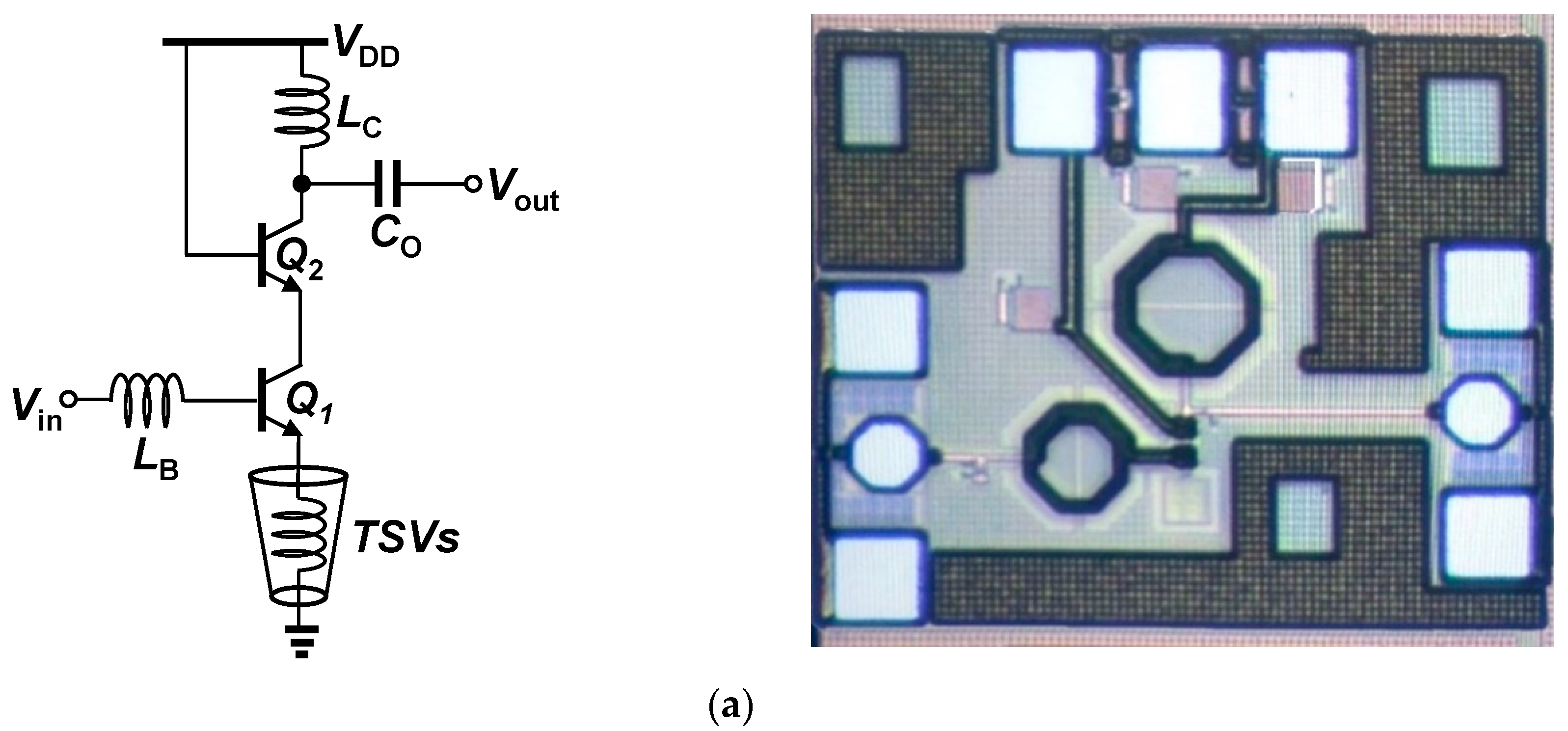
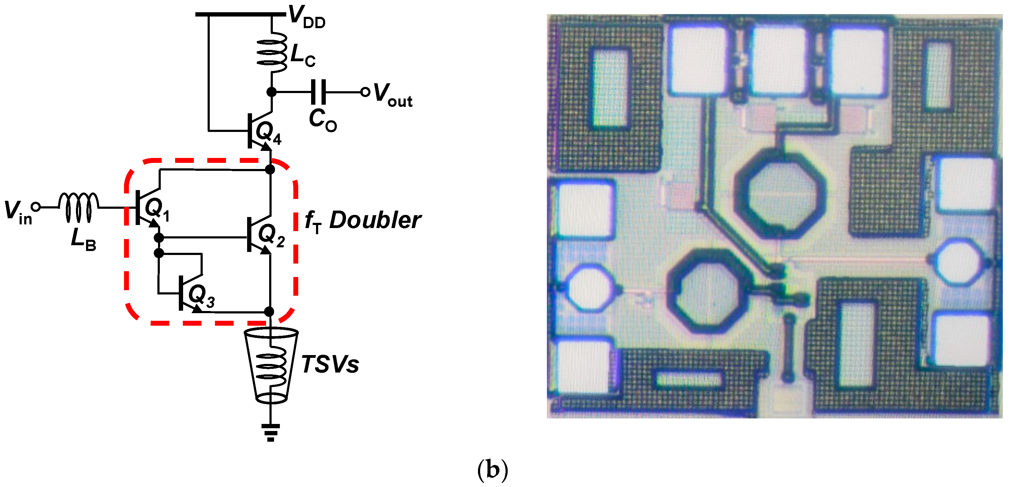
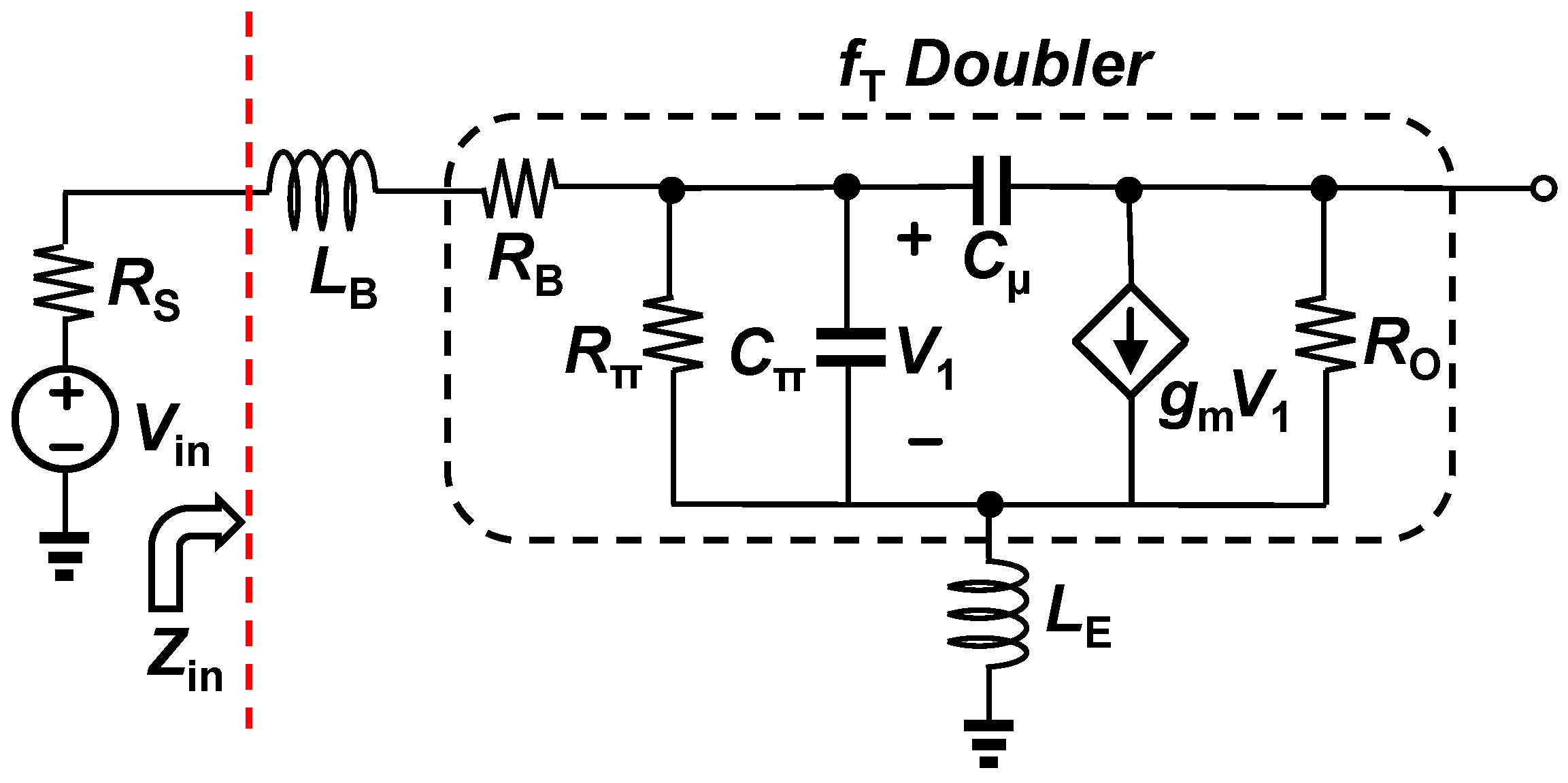
2. Proposed fT-Doubler RF Amplifier with TSVs

In the proposed fT-doubler amplifier, the fT-doubler cell (the red box in Figure 1b) is used in the input CE stage, and a single transistor is used as the cascode stage (Q4 in Figure 1b), whereas the conventional cascode topology is shown in Figure 1a. The fT-doubler CE stage, which can be modeled as a single transistor [14,15], is realized by using a modified Darlington pair, wherein two transistors, Q1 and Q2, are connected in series, with an additional diode-connected transistor, Q3, which adaptively adjusts the base-to-emitter voltage of Q2 for a different DC bias condition or a large AC signal. In the proposed circuit, Q1 and Q2 are biased with the same (or almost similar) currents so that the transconductance (gm) of both devices remain close to each other to maximize RF performance. The higher gain of the proposed amplifier is achieved by the Darlington operation, whose overall current gain of the fT-doubler cell is given by the product of current gain β1 and β2 of Q1 and Q2, respectively.
β f T   d o u b l e r   β 1 × β 2
The amplified collector current enters the emitter of the CB transistor and exits the collector with a unity current gain in an ideal case. The collector current is converted to a voltage by the load impedance at the collector of the CB transistor. Due to the high output resistance of the cascode topology, the overall impedance is determined by the output collector inductor (LC).
A TSV provides a low-loss electrical connection from the top side of the silicon substrate to the backside, and it is used to present a direct path to ground, eliminating a bonding wire and its parasitics. For simplicity, a TSV can be modeled as a negligible small resistance in series with an inductance [18]. At high frequencies, this inductance associated with a TSV can be used to design impedance matching and optimize noise figure. TSVs can form an array of shapes to adjust the effective resistance and inductance, and as a result, the number of TSVs can be selected based on the required inductance for design optimization [16]. Although, due to the resistance and the inductance associated with TSVs at the emitter of the CE transistor, the gain of the amplifier can be degraded theoretically, typical resistance will be much smaller than a few ohms, which can be ignored in the small-signal equivalent circuit of the fT doubler, as shown in Figure 2.
For simplification of calculation, if we consider the small-signal model where Rπ is very high and Cµ is very small, the effective Gm with degeneration inductance is [20],
G m = g m ω 0 ( g m L E + C π R B )
In (2), L E , g m , R B , and ω 0 are emitter inductance, transconductance, base resistance, and the operation frequency, respectively. We can see that if the degeneration inductance ( L E ) increases, the effective G m decreases, so does the gain of the amplifier.

2.1. Input and Output Matching

The input and output matching networks affect the bandwidth and the power transfer between stages. In the proposed RFA, the input matching is accomplished using a series inductor ( L B ) and degeneration inductance ( L E ) in the TSV, achieving a higher gain and lower noise figure simultaneously. For input matching, the imaginary part of the input impedance should be zero, and the real part should be equal to 50 Ω. The input impedance of the amplifier can be found from Figure 2 and is derived as follows:
Z i n = [ 1 + s L E R π + s 2 L E C π + g m s L E + s L E ( s C µ g m ) ( 1 + s C µ R 0 ) 1 R π + s C π + s C µ s C µ ( s C µ g m ) ( 1 R 0 + g m ) + s L B + R B ]
where R π , C µ , L B , and R 0 are input resistance from base to emitter, base-to-collector capacitance, base series inductor for input matching, and the output resistance of the amplifier, respectively. Because of the complexity associated with (3), it is difficult to separate the real and the imaginary part with intuitive meanings for matching network design. If we simplify the small-signal model where R π = ,   r 0 = ,   a n d   C µ = 0 , then the simplified expression would be
Z i n = s L B + s L E + 1 s C π + R B + g m L E C π
From (4), it can be realized that the value of L E of a TSV can be adjusted to achieve the 50 Ω real input impedance. This will eliminate the use of an extra on-chip emitter inductor or transmission line, which reduces the overall chip area as well. The output matching was straightforward, where collector inductor ( L C ) and output capacitor ( C o ) are tuned to resonate at the operation frequency.

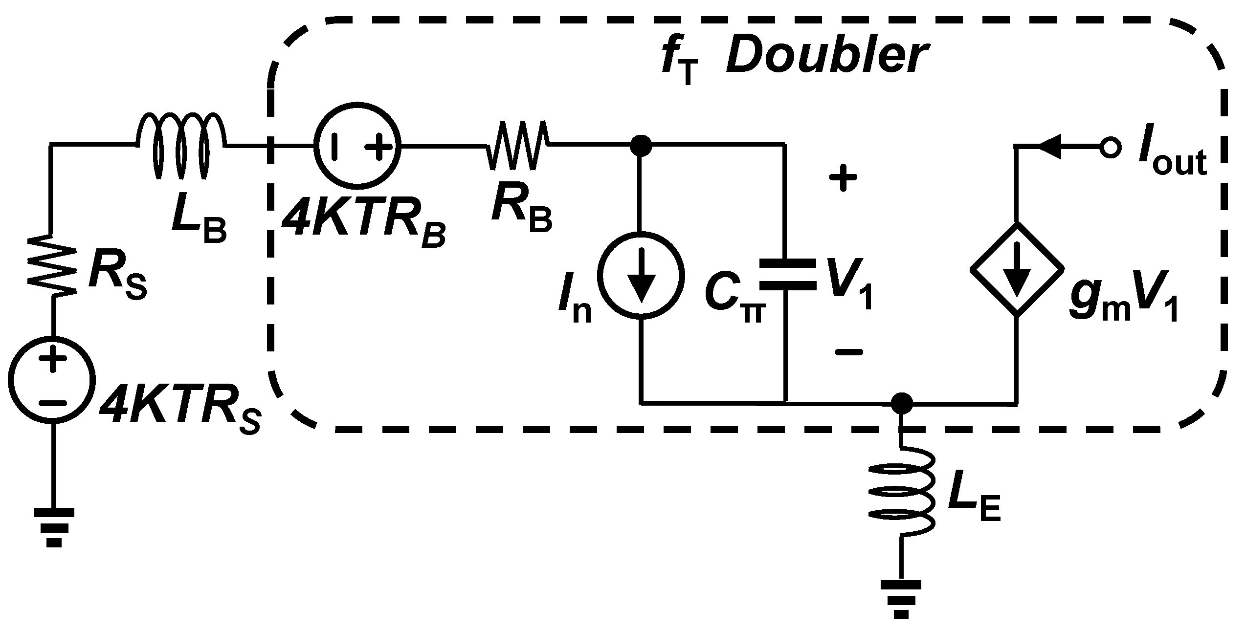
2.2. Noise Figure Calculation

The overall noise figure (NF) of the amplifier will heavily depend upon the noise performance of the input stage (i.e., fT-doubler cell) in the proposed amplifier since the noise contribution from the cascode CB stage is relatively smaller [21]. The main noise sources of a SiGe HBT is the noise generated at the base due to the base resistance and the base-emitter shot noise, whereas for the inductive degenerated amplifiers, the contribution of the collector-to-emitter noise is relatively smaller [22]. The NF of the proposed amplifier can be calculated by using the simplified small-signal noise model, as shown in Figure 3.
The NF of the proposed amplifier under impedance-matched conditions can be derived as follows [20,23,24],
N F = 1 + R B R S + q I B 2 k T R S   [ ( R B + R S ) 2 + ω 0 2 ( L B + L E ) 2 ]
Here, q, k, T, and I B are electron charge, Boltzmann constant, absolute temperature, and the base bias current, respectively. The NF of the proposed fT-doubler RFA will be degraded from that of conventional cascode amplifiers because R B in the fT-doubler cell is almost twice of that of single HBTs [14]. From (5), it is shown that by optimizing the number of TSVs, L E can be adjusted for balancing both input matching and noise performance.

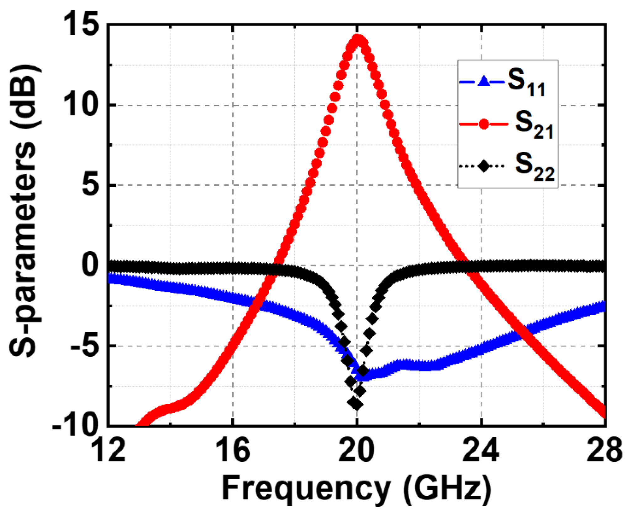
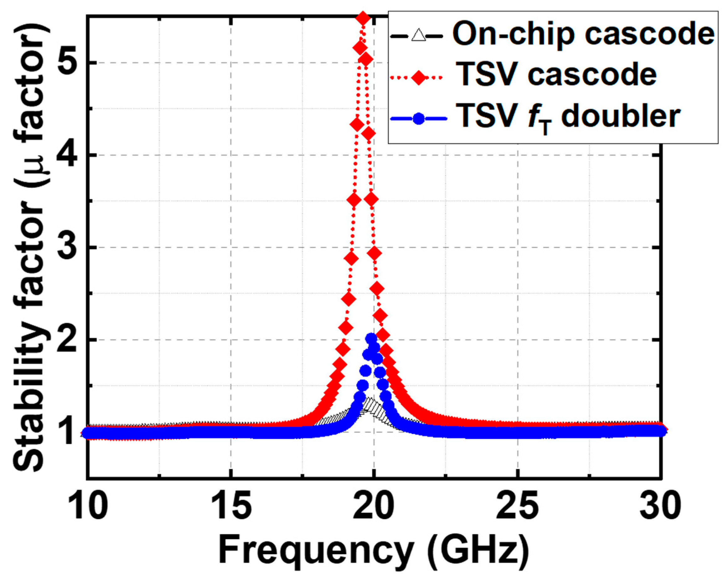
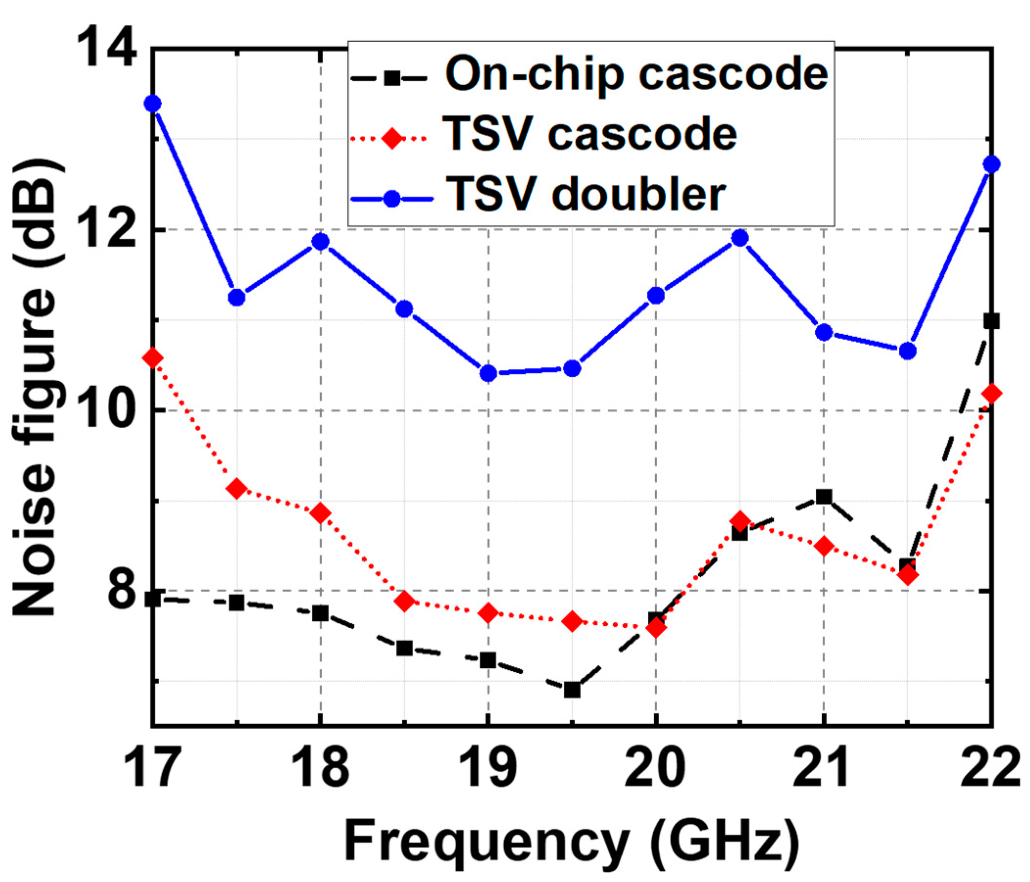
3. Measurement Results and Discussion

The proposed TSV-integrated fT-doubler RF amplifiers (RFAs) were designed and fabricated for K-band operation, using a commercial 0.35-µm SiGe HBT technology [17], whose fT and the maximum oscillation frequency (fmax) are in the range of 30 GHz and 60 GHz, respectively [25,26]. The scattering parameters (S-parameters) and the NF were measured using a network analyzer (Agilent PNA E8364B) and a signal analyzer (Agilent PXA N9030A) with a noise source (Agilent N4002A), respectively. For comparison purposes, three RFAs (on-chip conventional, TSV-integrated conventional, and the proposed TSV-integrated fT-doubler RFAs) were characterized. The schematic and the chip micrograph of the TSV-integrated conventional and the proposed fT-doubler RFAs are shown in Figure 1.
The measured S-parameter response of the proposed TSV-integrated fT-doubler RFA under a fixed bias current of 1.1 mA is shown in Figure 4. For measurement purposes, the DC and RF probes shared the ground potential through the on-chip ground mesh, but they were isolated from the TSV ground, which was provided from the chuck of the probe station. The proposed RFA had a peak gain of 14.11 dB at the center frequency of 20 GHz, and the 3-dB gain bandwidth was about 1.3 GHz. The input and the output ports were matched around the peak gain frequency, showing broader input matching due to the lower Q-factor from the small-base resistance than the output.
Figure 5 shows the gain (S21) comparison of the three RFAs versus frequency. The TSV-integrated conventional cascode RFA shows a slight degradation (0.8 dB) in gain compared with the on-chip conventional RFA. This is due to the presence of large parasitics at the interface between the backside of TSVs and the probe station chuck. Since the TSV-integrated fT-doubler RFA provides an additional gain (or increased fT), it shows that the proposed approach is a viable solution for gain boosting with compact size. The proposed RFA has a gain increase of 3.7 dB from that of the conventional TSV-integrated amplifier. In addition, the stability (µ factor) of our proposed RFA was confirmed over a wide range of frequency (10–30 GHz) and compared with the conventional cascode amplifiers (Figure 6).
The noise performance of the proposed RFA is shown in Figure 7. The NF of the proposed RFA was degraded by 4.3 dB at 20 GHz from the conventional TSV-integrated cascode topology due to a larger RB. Since the high-frequency metrics (fT and fMAX) of the given process was conservative, however, the resulting lowest NF of the conventional cascode RFA as well as the proposed RFA was inevitably high (6.5 dB and 10.4 dB, respectively) at 20 GHz compared with typical low-noise amplifiers in a similar frequency range in the literature. With more advanced SiGe BiCMOS technologies [27], it is expected that the NF will show a more significant improvement than the noise performance of the RFA prototypes.
In Table 1, the performance parameters of the proposed RFAs and the conventional cascode RFA are summarized. The improved gain or extended frequency range of the proposed fT-doubler RFA with the advantage of a reduced chip area was achieved with a tradeoff in NF and power consumption. With the use of advanced scaled transistors, the performance of the fT-doubler-based amplifier can certainly improve maintaining a reasonable NF performance.
The fabricated RFAs were irradiated by an x-ray source for characterizing radiation-induced degradations. The RFAs were still functional after exposure to a total dose of 1 Mrad (SiO2). The TID x-ray irradiation results of the TSV-integrated conventional cascode and the proposed RFAs are summarized in Table 2.

4. Conclusions

This work presents an improvement in the gain of radio-frequency amplifiers (RFAs) for high-performance applications by using the fT-doubler cell as an input stage. Whereas there is a tradeoff in noise figure and power consumption in the proposed RFA, the peak gain increases significantly, demonstrating extended usable frequency range. In addition, the use of TSVs as impedance-matching elements enables the elimination of a transmission-line structure or a lumped inductor, potentially reducing the overall chip area.

Author Contributions

Conceptualization, I.S.; methodology, I.S.; validation, M.A.R.S. and I.S.; formal analysis, M.A.R.S. and I.S.; investigation, I.S.; data curation, I.S.; writing—original draft preparation, M.A.R.S.; writing—review and editing, I.S.; visualization, M.A.R.S.; supervision, I.S.; All authors have read and agreed to the published version of the manuscript.

Funding

This research received no external funding.

Conflicts of Interest

The authors declare no conflict of interest.

References

  1. Cressler, J.D. Radiation effects in SiGe technology. IEEE Trans. Nucl. Sci. 2013, 60, 1992–2014. [Google Scholar] [CrossRef]
  2. Cressler, J.D. Silicon-Germanium as an enabling technology for extreme environment electronics. IEEE Trans. Device Mater. Reliab. 2010, 10, 437–448. [Google Scholar] [CrossRef]
  3. Banerjee, G.; Niu, G.; Cressler, J.D.; Clark, S.D.; Palmer, M.J.; Ahlgren, D.C. Anomalous dose rate effects in gamma irradiated SiGe heterojunction bipolar transistors. IEEE Trans. Nucl. Sci. 1999, 46, 1620–1626. [Google Scholar] [CrossRef]
  4. Zhang, J.; Guo, Q.; Guo, H.; Lu, W.; He, C.; Wang, X.; Li, P.; Liu, M. Impact of bias conditions on total ionizing dose effects of 60Coγ in SiGe HBT. IEEE Trans. Nucl. Sci. 2016, 63, 1251–1258. [Google Scholar] [CrossRef]
  5. Cressler, J.D.; Mantooth, H.A. Extreme Environment Electronics; CRC Press: Boca Raton, FL, USA, 2012. [Google Scholar]
  6. Shen, P.; Zhang, W.; Xie, H.; Jin, D.; Zhang, W.; Li, J.; Gan, J. An ultra-wideband darlington low noise amplifier design based on SiGe HBT. In Proceedings of the International Conference on Microwave and Millimeter Wave Technology, Nanjing, China, 21–24 April 2008; Volume 3, pp. 1372–1375. [Google Scholar] [CrossRef]
  7. Paek, J.-S.; Park, B.; Hong, S. CMOS LNA with darlington-pair for UWB systems. Electron. Lett. 2006, 42, 913–914. [Google Scholar] [CrossRef]
  8. Elahipanah, H.; Salemi, A.; Zetterling, C.-M.; Östling, M. Intertwined design: A novel lithographic method to realize area efficient high-voltage SiC BJTs and darlington transistors. IEEE Trans. Electron Devices 2016, 63, 4366–4372. [Google Scholar] [CrossRef]
  9. Nikandish, G.; Medi, A. Design and analysis of broadband Darlington amplifiers with bandwidth enhancement in GaAs pHEMT technology. IEEE Trans. Microw. Theory Tech. 2014, 62, 1705–1715. [Google Scholar] [CrossRef]
  10. Weng, S.-H.; Chang, H.-Y.; Chiong, C.-C.; Wang, Y.-C. Gain-bandwidth analysis of broadband darlington amplifiers in HBT-HEMT process. IEEE Trans. Microw. Theory Tech. 2012, 60, 3458–3473. [Google Scholar] [CrossRef]
  11. Krishnamurthy, K.; Vetury, R.; Keller, S.; Mishra, U.; Rodwell, M.J.; Long, S.I. Broadband GaAs MESFET and GaN HEMT resistive feedback power amplifiers. IEEE J. Solid-State Circuits 2000, 35, 1285–1292. [Google Scholar] [CrossRef] [Green Version]
  12. Feghhi, R.; Joodaki, M. Realization of a broadband hybrid X-band power amplifier based on fT-doubler technique. AEU-Int. J. Electron. Commun. 2019, 104, 119–127. [Google Scholar] [CrossRef]
  13. El-Gabaly, A.M.; Stewart, D.; Saavedra, C.E. 2-W broadband GaN power-amplifier RFIC using the fT doubling technique and digitally assisted distortion cancellation. IEEE Trans. Microw. Theory Tech. 2013, 61, 525–532. [Google Scholar] [CrossRef]
  14. Yuan, J.; Cressler, J.D. Enhancing the speed of SiGe HBTs using fT-Doubler techniques. In Proceedings of the IEEE Topical Meeting on Silicon Monolithic Integrated Circuits in RF Systems, Orlando, FL, USA, 23–25 January 2008; pp. 50–53. [Google Scholar] [CrossRef]
  15. Jain, V.; Gross, B.J.; Pekarik, J.J.; Adkisson, J.W.; Camillo-Castillo, R.A.; Liu, Q.; Gray, P.B.; Vallett, A.; Divergilio, A.W.; Zetterlund, B.K.; et al. Investigation of HBT Layout Impact on fT Doubler Performance for 90 nm SiGe HBTs. In Proceedings of the IEEE Bipolar/BiCMOS Circuits and Technology Meeting (BCTM), Coronado, CA, USA, 28 September–1 October 2014; pp. 5–8. [Google Scholar] [CrossRef]
  16. Song, I.; Cho, M.-K.; Jung, S.; Ju, I.; Cressler, J.D. Advantages of utilizing through-silicon-vias in SiGe HBT RF low-noise amplifier design. Microw. Opt. Tech. Lett. 2015, 57, 2703–2706. [Google Scholar] [CrossRef]
  17. Joseph, A.J.; Gillis, J.D.; Doherty, M.; Lindgren, P.J.; Previti-Kelly, R.A.; Malladi, R.M.; Wang, P.-C.; Erturk, M.; Ding, H.; Gebreselasie, E.G.; et al. Through-silicon vias enable next-generation SiGe power amplifiers for wireless communications. IBM J. Res. Dev. 2008, 52, 635–648. [Google Scholar] [CrossRef]
  18. Tian, W.; Ma, T.; Liu, X. TSV Technology and high-energy heavy ions radiation impact review. Electronics 2018, 7, 112. [Google Scholar] [CrossRef] [Green Version]
  19. Liao, H.-Y.; Chiou, H.-K. RF model and verification of through-silicon vias in fully integrated SiGe power amplifier. IEEE Electron Device Lett. 2011, 32, 809–811. [Google Scholar] [CrossRef]
  20. Razavi, B. RF Microelectronics, 2nd ed.; Prentice Hall: Upper Saddle River, NJ, USA, 2011. [Google Scholar]
  21. Song, I.; Koo, M.; Jung, H.; Jhon, H.-S.; Shin, H. Optimization of cascode configuration in CMOS low-noise amplifier. Microw. Opt. Tech. Lett. 2008, 50, 646–649. [Google Scholar] [CrossRef]
  22. Girlando, G.; Palmisano, G. Noise figure and impedance matching in RF cascode amplifiers. IEEE Trans. Circuits Syst. II Analog Digit. Signal Process. 1999, 46, 1388–1396. [Google Scholar] [CrossRef]
  23. Cressler, J.D.; Niu, G. Silicon-Germanium Heterojunction Bipolar Transistors; Artech House: Norwood, MA, USA, 2002. [Google Scholar]
  24. Harame, D.; Larson, L.; Case, M.; Kovacic, S.; Voinigescu, S.; Tewksbury, T.; Nguyen-Ngoc, D.; Stein, K.; Cressler, J.; Jeng, S.-J.; et al. SiGe HBT technology: Device and application issues. In Proceedings of the International Electron Devices Meeting, Washington, DC, USA, 10–13 December 1995; pp. 731–734. [Google Scholar] [CrossRef]
  25. Joseph, A.; Liu, Q.; Hodge, W.; Gray, P.; Stein, K.; Previti-Kelly, R.; Lindgren, P.; Gebreselasie, E.; Voegeli, B.; Candra, P.; et al. A 0.35 μm SiGe BiCMOS technology for power amplifier applications. In Proceedings of the IEEE Bipolar/BiCMOS Circuits and Technology Meeting, Boston, MA, USA, 30 September–2 October 2007; pp. 198–201. [Google Scholar] [CrossRef]
  26. Seif, M.; Pascal, F.; Sagnes, B.; Elbeyrouthy, J.; Hoffmann, A.; Haendler, S.; Chevalier, P.; Gloria, D. Characterization, Modeling and Comparison of 1/f Noise in Si/SiGe:C HBTs Issued from Three Advanced BiCMOS Technologies. In Proceedings of the 29th International Conference on Microelectronics (ICM), Beirut, Lebanon, 10–13 December 2017; pp. 1–4. [Google Scholar] [CrossRef]
  27. Melai, J.; Magnée, P.; Pouwel, I.; Weijs, P.; Brunets, I.; van Dalen, R.; Vohra, A.; Tiemeijer, L.; Pijper, R.; Tuinhout, H.; et al. QUBiC generation 9, a new BiCMOS process optimized for mmWave applications. In Proceedings of the 2015 IEEE Bipolar/BiCMOS Circuits and Technology Meeting-BCTM, Boston, MA, USA, 26–28 October 2015; pp. 113–116. [Google Scholar] [CrossRef]
Figure 1. (a) Schematic and micrograph of the conventional through-silicon vias (TSV)-integrated unity-gain frequency (fT)-doubler amplifier; (b) the schematic of the proposed TSV-integrated cascode Silicon-germanium (SiGe) heterojunction bipolar transistor (HBT) amplifier (biasing is not shown).
Electronics 09 00772 g001aElectronics 09 00772 g001b
Figure 2. Equivalent small-signal model of the proposed TSV-integrated RF fT-doubler amplifier.
Electronics 09 00772 g002
Figure 3. Simplified small-signal noise model of the proposed TSV-integrated fT-doubler amplifier.
Electronics 09 00772 g003
Figure 4. Measured S-parameters of the TSV integrated fT-doubler radio-frequency amplifier (RFA).
Electronics 09 00772 g004
Figure 5. Comparison gain (S21) between the on-chip RFAs and TSV-integrated RFAs.
Electronics 09 00772 g005
Figure 6. Stability factor (µ factor) of the proposed fT-doubler and conventional cascode RFAs.
Electronics 09 00772 g006
Figure 7. NF comparison between the proposed fT-doubler and conventional cascode RFAs.
Electronics 09 00772 g007
Table 1. Performance Summary.
RFA Typefcenter (GHz)Gain (dB)NF (dB)PDC (mW)
On-chip conventional cascode19.611.26.61.8
TSV conventional cascode19.410.46.91.8
Proposed TSV fT-doubler20.014.111.23.3
Table 2. X-ray Irradiation Results.
RFA TypeGainNFPDC
TSV cascode−2.3 dB+0.40 dB<+2%
fT-doubler cascode−2.9 dB+0.43 dB<+2%

