Article

An Optimized Structure of Split-Gate Resurf Stepped Oxide UMOSFET

1
Institute of Microelectronics of Chinese Academy of Sciences, Beijing 100029, China
2
School of Microelectronics, University of Chinese Academy of Sciences, Beijing 100049, China
3
College of Electronic Science and Technology, Faculty of Information Technology, Beijing University of Technology, Beijing 100124, China
*
Author to whom correspondence should be addressed.
Electronics 2020, 9(5), 745; https://doi.org/10.3390/electronics9050745
Submission received: 19 April 2020 / Revised: 29 April 2020 / Accepted: 29 April 2020 / Published: 1 May 2020
(This article belongs to the Section Microelectronics)

Abstract

:
In this paper, a split-gate resurf stepped oxide with double floating electrodes (DFSGRSO) U-shape metal oxide semiconductor field-effect transistor (UMOSFET) is proposed. The floating electrodes are symmetrically distributed on both sides of the source electrode in the trench. The performance of the DFSGRSO UMOSFET with different size of floating electrodes is simulated and analyzed. The simulation results reveal that the floating electrodes can modulate the distribution of the electric field in the drift area, improving the performance of the device significantly. The breakdown voltage (BV) and figure of merit (FOM) of the DFSGRSO UMOSFET at optimal parameters are 23.6% and 53.1% higher than that of the conventional structure. In addition, the regulatory mechanism of the floating electrodes is analyzed. The electric field moves from the bottom of the trench to the middle of the drift area, which brings a new electric field peak. Therefore, the distribution of the electric field is more uniform for the DFSGRSO UMOSFET compared with the conventional structure.

1. Introduction

The power metal oxide semiconductor field-effect transistor (MOSFET) has been playing an important role in the electronic power industry with the development of society. In order to improve the performance of devices, some new structures have been proposed, such as the laterally-diffused MOSFET (LDMOSFET) [1,2,3], the vertical double-diffused MOSFET (VDMOFET) [3,4,5,6] and the U-shape MOSFET (UMOSFET) [6,7,8,9], and the on-state resistance (RSP) of these devices is getting lower and lower. However, it was difficult to realize a very low RSP due to the limit of one-dimensional silicon, until the super junction MOSFET (SJ-MOSFET) [10,11,12,13,14] was proposed. The RSP is about 140 mΩ·cm2–100 mΩ·cm2 [3,5] for the previous structure, while the SJ-MOSFET achieves an RSP of 10 mΩ·cm2, and the next-generation devices are likely to be around 8 mΩ·cm2 [11]. The SJ-MOSFET adopts the principle of charge-coupling, which could increase the doping concentration of the drift area, completely breaking the one-dimensional silicon limit and significantly improving the performance of the device. However, there are some problems in the actual process, mainly because of the doping interdiffusion. Therefore, the split-gate resurf stepped oxide (SGRSO) UMOSFET [14,15,16,17,18,19] has attracted the attention of researchers, as it also adopts the principle of charge-coupling and has a relatively simple preparation process compared with SJ-MOSFET. The conventional structure is shown in Figure 1a, whereby the electrode in the trench is connected to the source, which can enhance the depletion of drift area and increase the doping concentration of the epitaxial layer to reduce the RSP of the device.
However, the electric field distribution of this structure is not very ideal compared with the SJ-MOSFET, especially for breakdown above 200 V [20]. In order to improve the distribution of electric field in the drift area, a series of measures has been put forward, for example, a split gate UMOSFET with P-pillar [21], subsection dielectric layer [22] and slope oxide layer [23], but it is unclear if the control of the slope side oxygen or P-pillar is feasible with the appropriate accuracy in the actual process and so on. Hence, an advanced SGRSO UMOSFET with a higher breakdown voltage (BV) and figure of merit (FOM) is needed.
In this paper, a split-gate resurf stepped oxide with double floating electrodes (DFSGRSO) UMOSFET is proposed. The floating electrodes are symmetrically distributed on both sides of the source electrode in the trench. The simulation results reveal that the BV and FOM at optimal parameters are higher than those of the conventional structure. In addition, the performance of the DFSGRSO UMOSFET with different size of floating electrodes and the regulatory mechanism of the floating electrodes is analyzed in this paper.

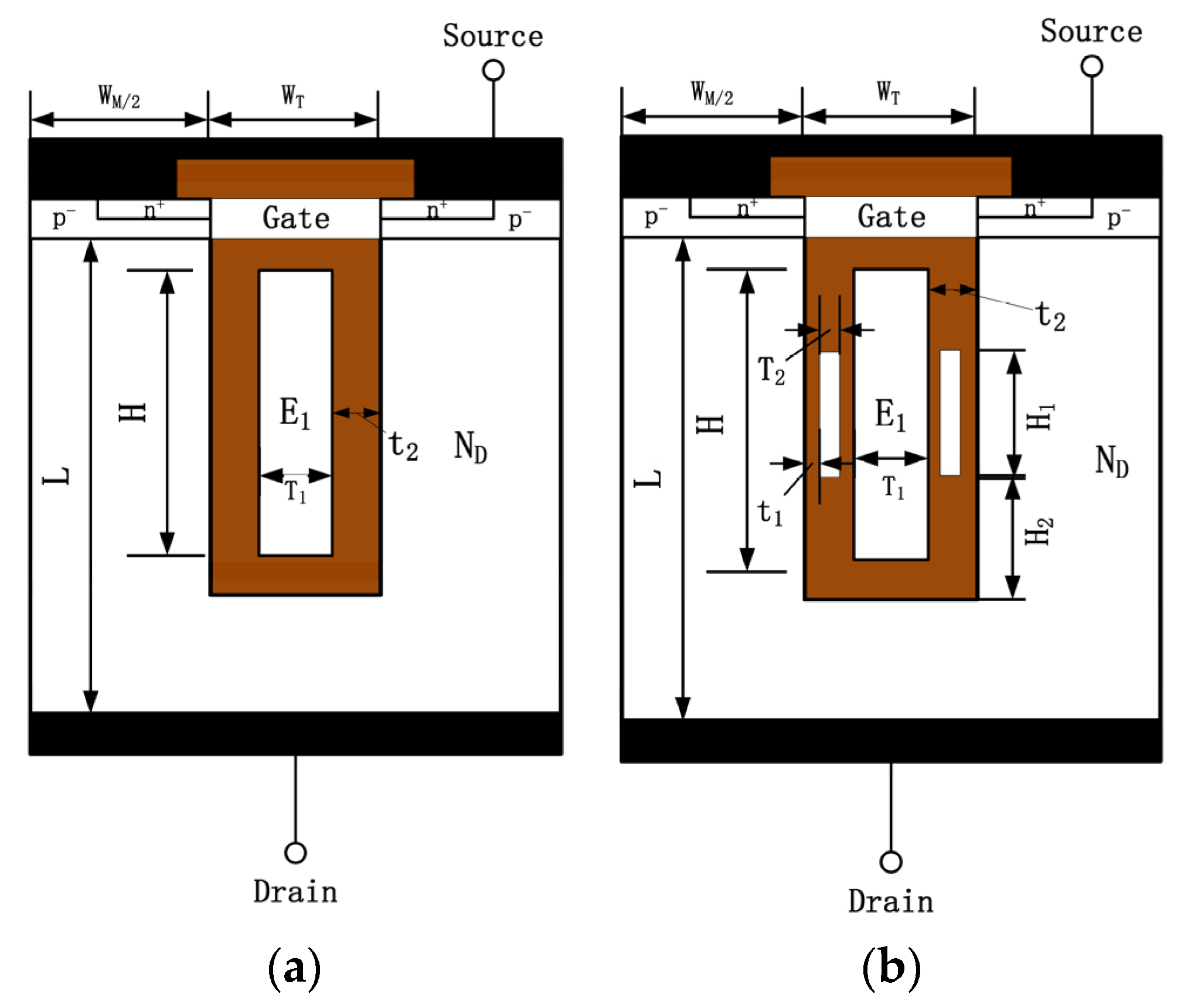
2. Device Structure and Principles of Operation

The schematic of the DFSGRSO UMOSFET is shown in Figure 1b. The electrode in the trench (E1) is connected to the source electrode in order to achieve charge-coupling. Two floating electrodes are introduced in the trench and located on both sides of the source electrode (E1) symmetrically. The floating electrodes and the source electrode (E1) are separated by the oxide layer. Except for the floating electrodes of the DFSGRSO UMOSFET, the other structural parameters are the same as the conventional structure.
As shown in Figure 2, the distribution of the electric field and potential of the DFSGRSO UMOSFET are compared with that of the device with the conventional structure. As shown in Figure 2a,b, the electric field distribution of the DFSGRSO UMOSFET is more uniform compared to the conventional structure, which reveals that the floating electrodes can modulate the electric field of the drift area. The floating electrodes can be regarded as an equipotential body. Therefore, the electric field originally converged on the bottom of the trench moves to the middle of the drift area, which is near the top of the floating electrodes, and it brings a new electric field peak. Furthermore, it can be seen from Figure 2c,d that the introduction of a floating electrode can increase the density of the potential line, which proves that the DFSGRSO UMOSFET has a higher breakdown voltage at the same structural parameters.
As shown in the Figure 3, the electric field intensity on the surface of the trench and in the middle of the drift area for the DFSGRSO UMOSFET are compared with that for the conventional structure, respectively, at the same structure parameters. Figure 3a is a comparison of the electric field on the trench surface of the two structures. It can be clearly seen that a new electric field peak (A) has been brought, which is near the top of the floating electrode, while the intensity of the electric field, which is near the bottom of the floating electrode, has decreased. In addition, the electric field intensity in the middle of the drift area is compared, as shown in Figure 3b. It can be seen that the introduction of the floating electrode improves the intensity of peak 1 significantly, and the distribution of the electric field is more uniform compared with the conventional structure.
A three-dimensional views of the electric field distribution in the drift area of the two structures are shown in Figure 4. Figure 4a–d show the front view and back view of the SGRSO and DFSGRSO UMOSFETs respectively. The electric field distribution in the drift area of the DFSGRSO UMOSFET is more symmetrical compared with the conventional structure where the electric field usually converges at the bottom of the trench. As a result, the volume under the electric field curved surface of the DFSGRSO UMOSFET is bigger than that of the SGRSO UMOSFET. Hence, the DFSGRSO UMOSFET has a higher BV and FOM.

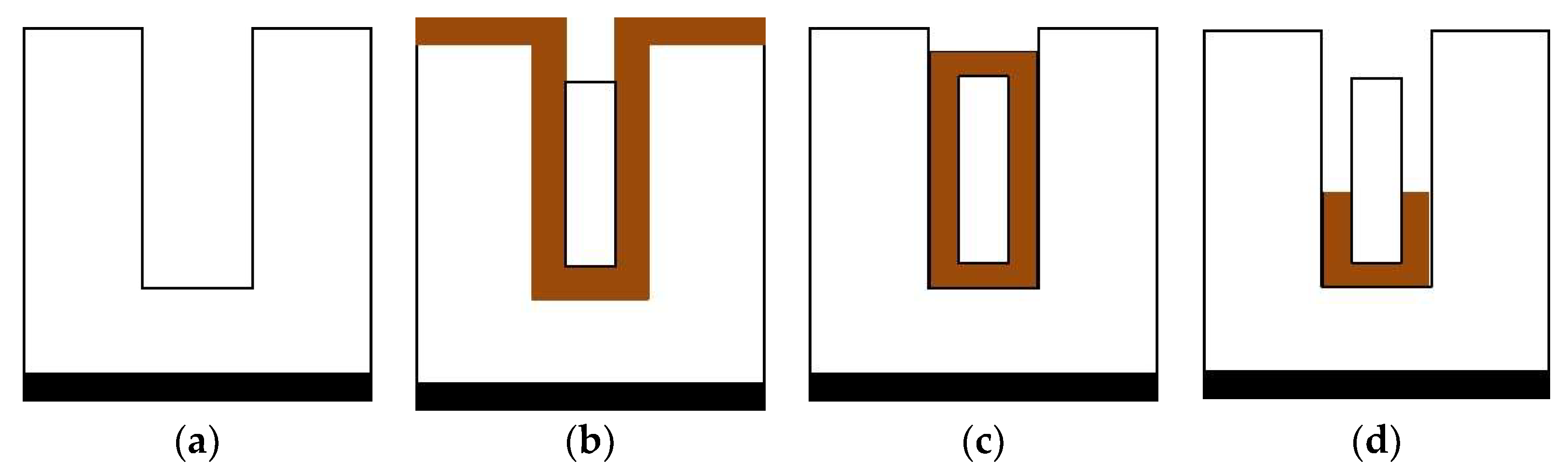
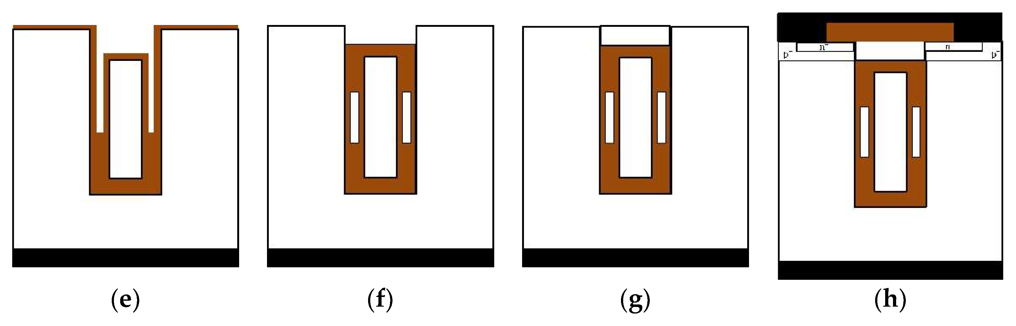
3. Fabrication Procedure

First, a N-type epitaxial layer grows on a heavily doped N+ substrate and a deep trench is formed by dry etching, as shown in Figure 5a. Next, a 1.2 µm oxide is deposited on the trench surface, as shown in Figure 5b. As can be seen in Figure 5c, the trench is filled with highly doped N-type polysilicon and etched back. Then, the trench is filled with oxide and etched back again to obtain the space for the floating electrodes, as shown in Figure 5d. As shown in Figure 5e, a thicker oxide is deposited on the surface of the trench. Afterwards, the trench is refilled with polysilicon and etched back to form the floating electrodes, as shown in the Figure 5f. Subsequently, a 50 nm fresh oxide is grown thermally on the trench sidewalls to form the gate oxide, and the gate is formed by the Chemical Mechanical Polishing (CMP) process, as shown in the Figure 5g. Finally, the n+ and p body is formed by the ion implantation, and the complete structure is shown in Figure 5h.

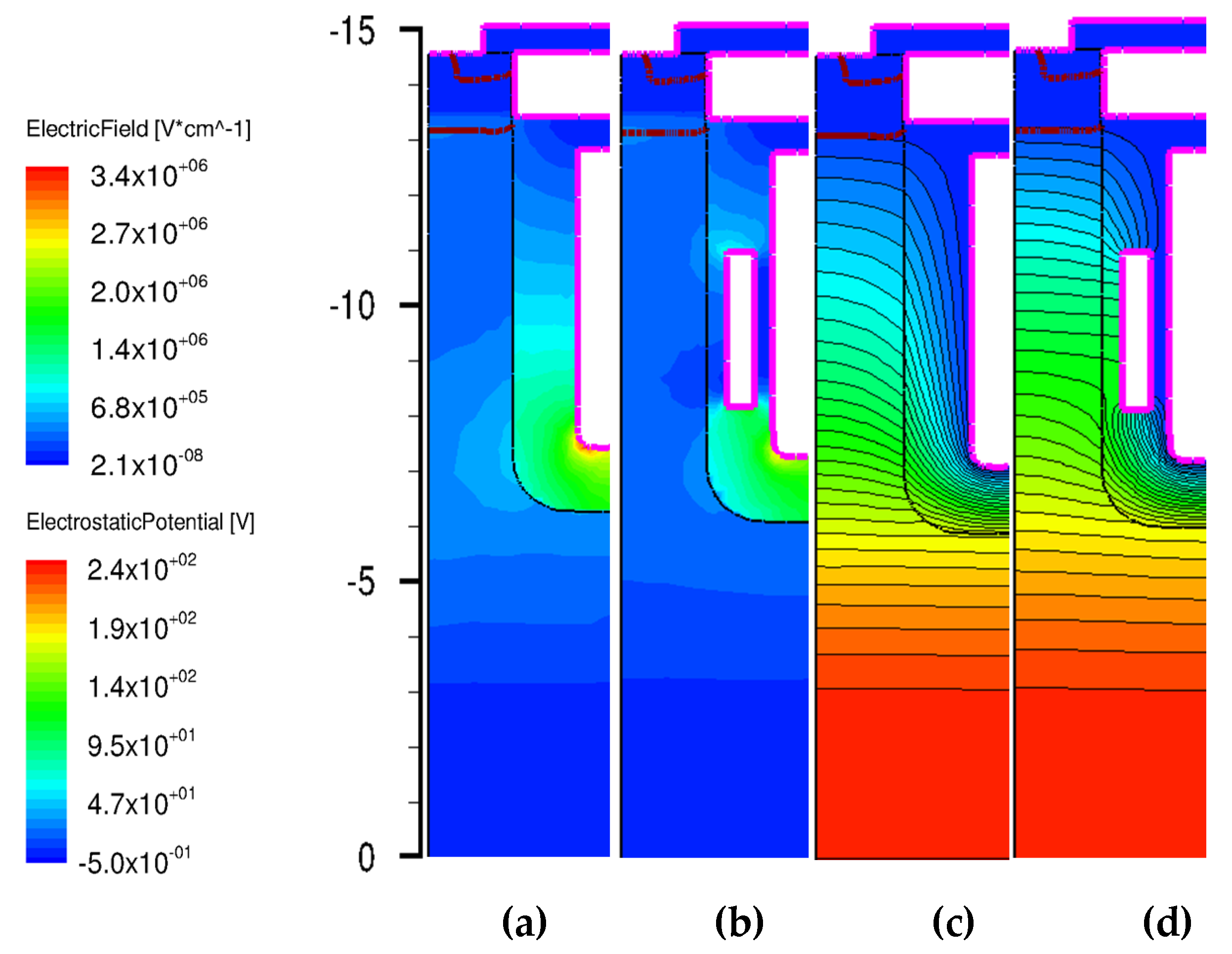
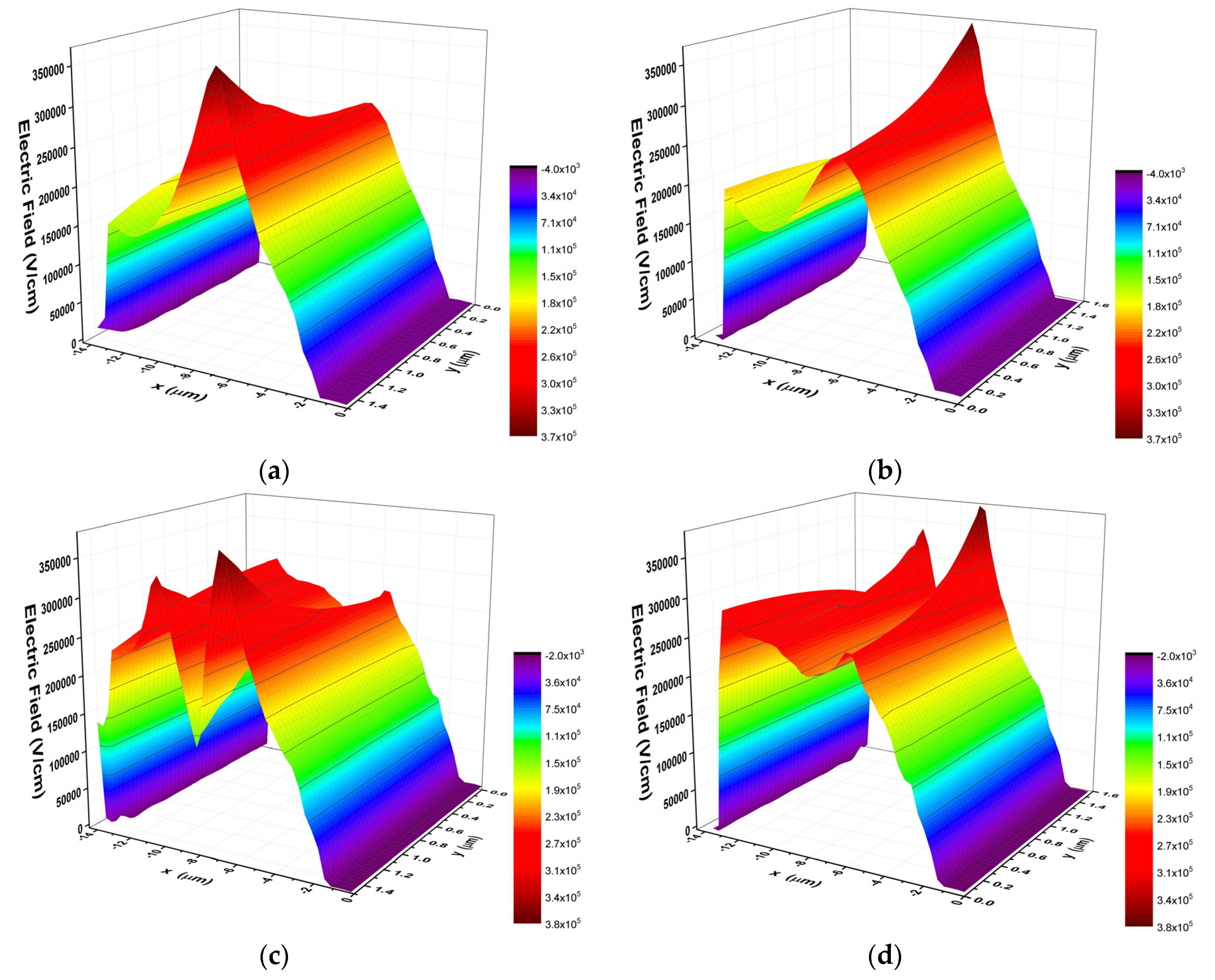
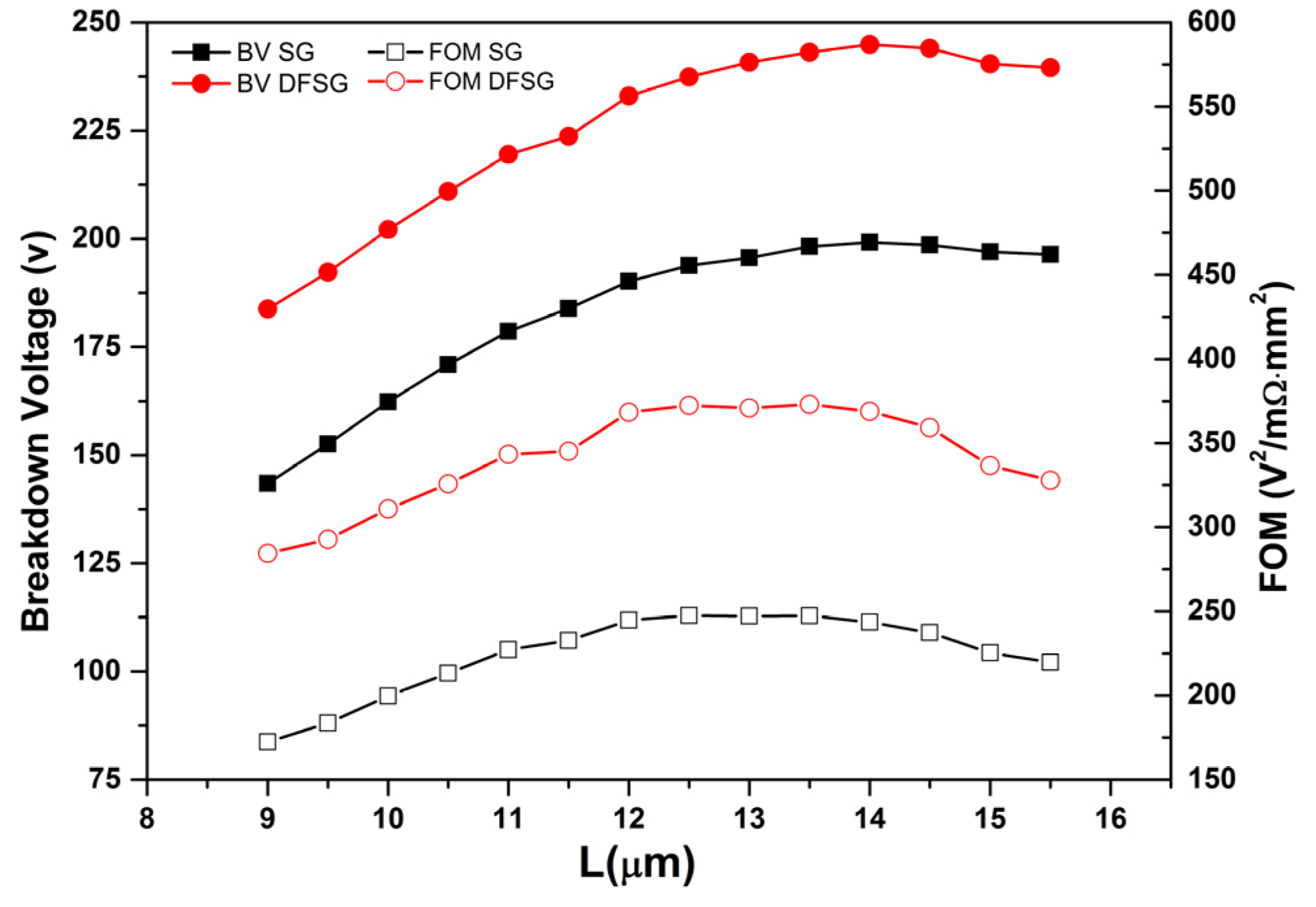
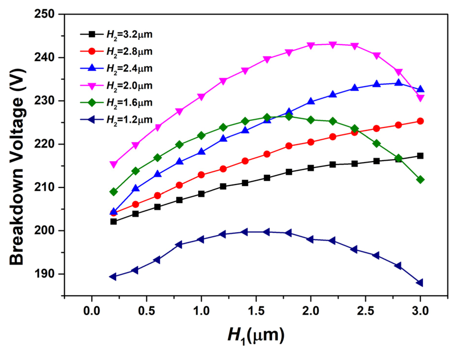
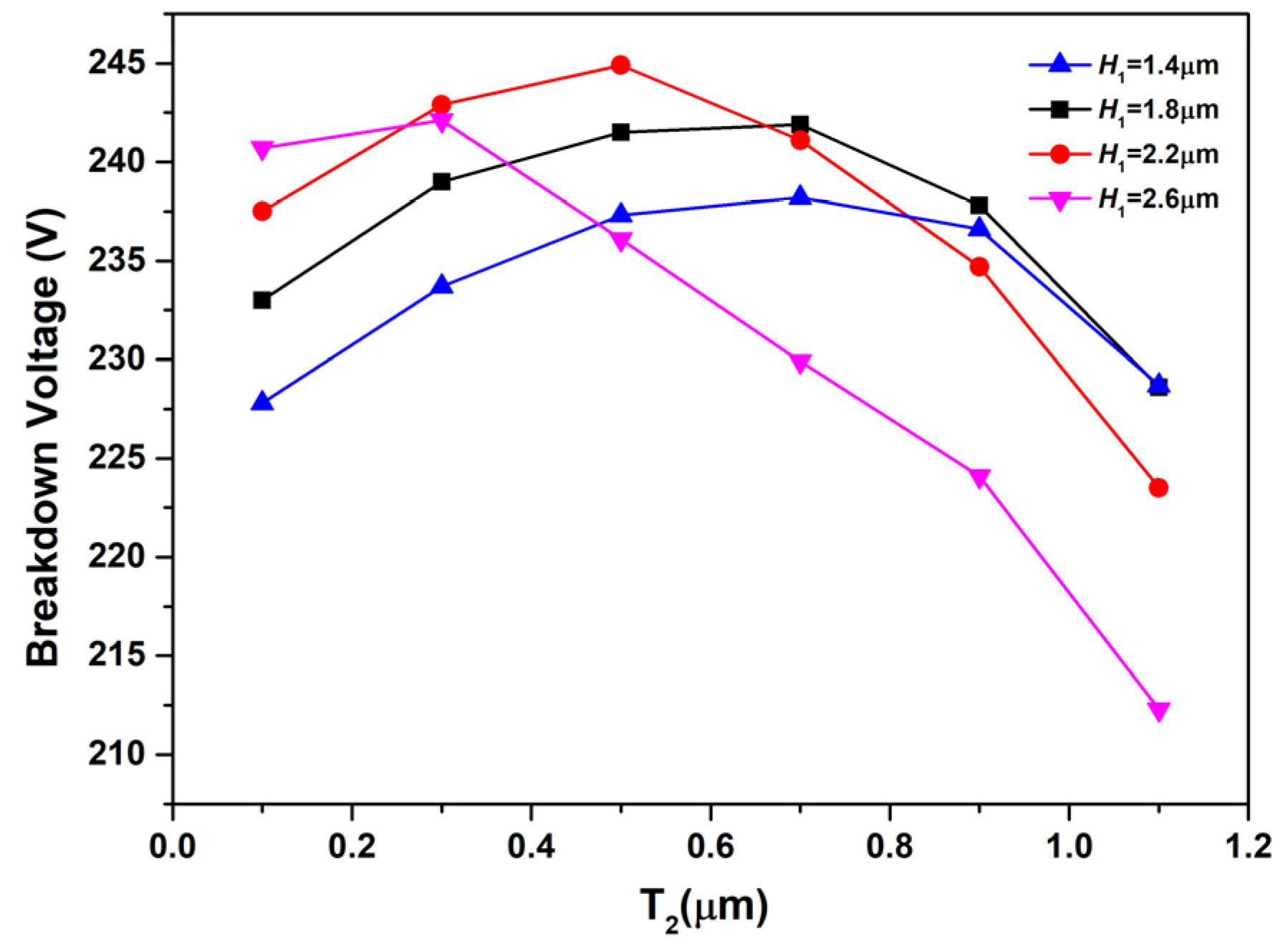
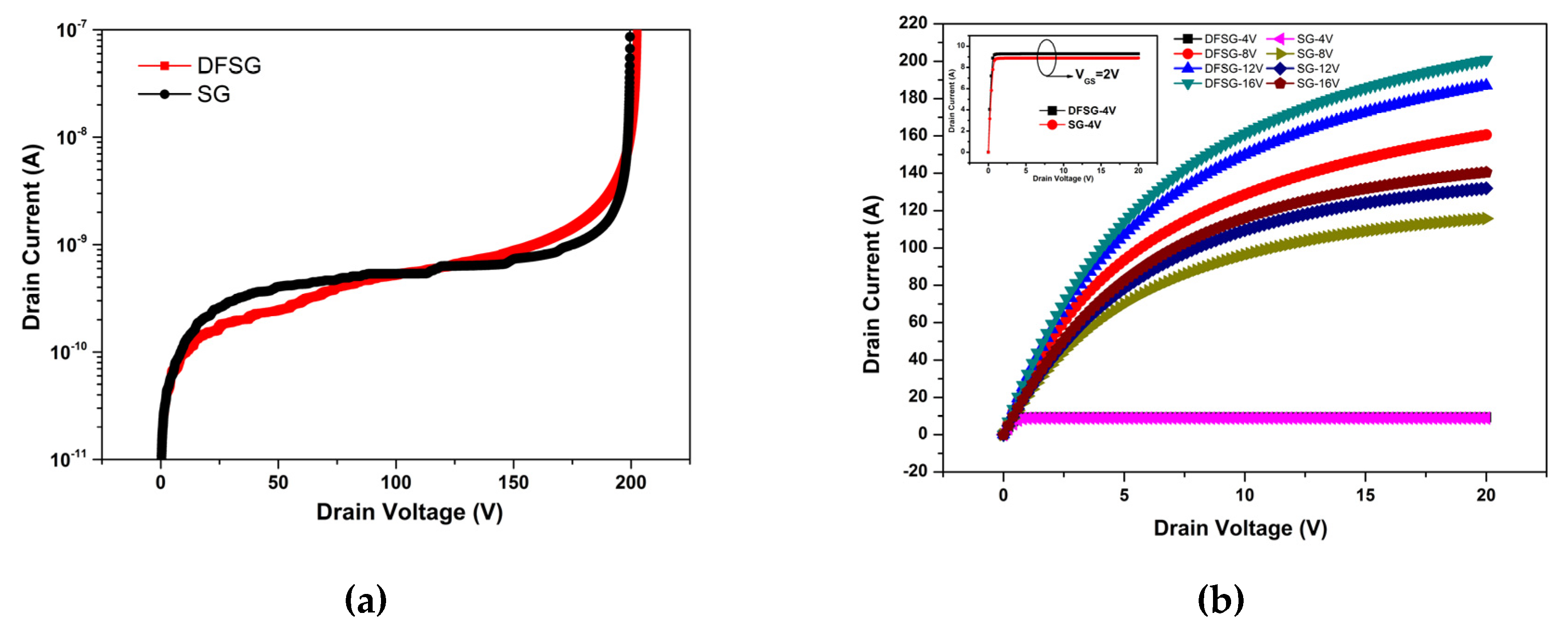
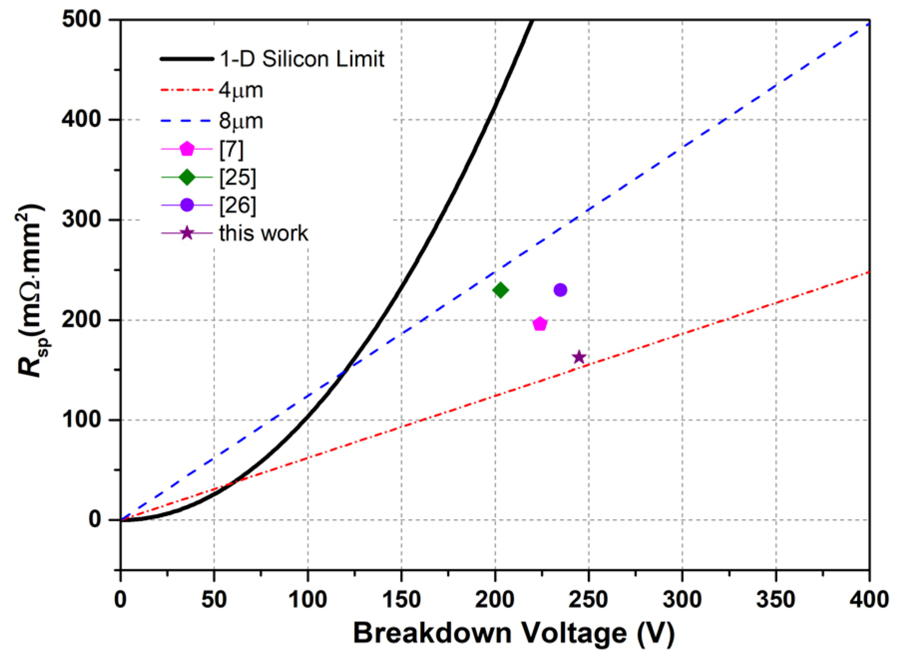
4. Results and Discussion

To compare the characters of both structures, we adopt the model of bandgap narrowing, the concentration dependent mobility model (CONMOB), the parallel electric field-dependent mobility model (FLDMOB) and the Shockley-Read-Hall model in simulations [24].
Figure 6 shows the dependence of the BV and FOM on the doping concentration of n-drift for the two structures. The parameters of the structures used in the simulations are shown in Table 1. It can be seen that the BV and FOM of the DFSGRSO UMOSFET are always higher than that of the conventional structure in the range of 1 × 1015 cm3–5 × 1015 cm3. With the increase of doping concentration, the BV of the two structures decreases gradually, but the FOM value increases and achieves the optimal value when the n-drift doping concentration is 4.5 × 1015 cm3. As a result, the BV and FOM of the conventional structure are 195.2 V and 236.1 V2/mΩ·mm2 respectively, while the BV and FOM of the DFSGRSO UMOSFET are 238.3 V and 352.7 V2/mΩ·mm2 respectively, which have been improved by 22.1% and 49.4%.
The dependence of the BV and FOM on the thickness of the epitaxial layer (L) for the SGRSO and DFSGRSO UMOSFETs is shown in the Figure 7. As can be seen from the figure, with the increase of the thickness of the epitaxial layer for the two structures, the BV reaches saturation state, while FOM increases gradually at first and then decreases after reaching the optimal value, because the on-state resistance gradually increases with the increase of the thickness of the epitaxial layer for both structures. As shown in the results, when the epitaxial layer thickness is 13.5 µm, the FOM of the two structures achieves the optimal value. Furthermore, the BV and FOM of the device with the conventional structure are 198.2 V and 247.3 V2/mΩ·mm2, while the BV and FOM of the DFSGRSO UMOSFET are 243.1 V and 373.1 V2/mΩ·mm2, which have been improved by 22.7% and 50.9% respectively.
The dependence of BV on the length of floating electrodes (H1) at different depth (H2) for the DFSGRSO UMOSFET is shown in Figure 8. Each curve in the figure represents the variation of the BV with the length of the floating electrodes at a certain depth for the DFSGRSO UMOSFET. It can be seen from the graph, at different depths, the BV of the DFSGRSO UMOSFET always increases gradually with the length of the floating electrodes at first and then decreases after reaching the optimal value. This is because as the length of the floating electrodes increases, the electric field gradually moves from the bottom of the trench to the middle of the drift area and achieves a uniform state. If the length of the floating electrodes continues to increase, the optimal state is broken, and the electric field around of the PN junction increases sharply. It makes the DFSGRSO UMOSFET break in advance and reduces the BV of the device. In addition, it can be seen from the graph that the modulation effect of the floating electrodes becomes stronger as its depth increases, and the length of floating electrodes required to achieve optimal station gradually reduces. When the depth and length of the floating electrodes is 2 µm and 2.2 µm respectively, the BV reaches a maximum value of 238.3 V. However, if the depth of the floating electrodes continues to increase, the BV of the DFSGRSO UMOSFET decreases due to the break of the charge-coupling.
Figure 9 shows the dependence of the BV on the width of the floating electrodes (T2) for different lengths (H1) for the DFSGRSO UMOSFET. Each curve in the figure represents the variation of the BV with the width of the floating electrodes at a certain length. As the width of the floating electrode increases, its BV gradually increases and reaches the optimal value. Furthermore, the trend of the BV with the length is similar to the result of Figure 8. As the length of the floating electrodes increases, the breakdown voltage of the device gradually increases, and the width required to reach the optimal value becomes smaller and smaller. When the length and width of the floating electrode is 2.2 µm and 0.5 µm, the BV and FOM of the DFSGRSO UMOSFET reaches the optimal values of 244.9 V and 378.6 V2/mΩ·mm2 respectively, which shows an improvement of 23.6% and 53.1% compared with the device with the conventional structure.
In order to compare the output characteristics of the two structures, the BV of both structures was set at about 200 V by adjusting the doping concentration of the drift area, as shown in the Figure 10a. The leakage current is limited to 1 × 10⁻⁷A. Figure 10b shows a comparison of the output characteristic for both structures. As can be seen from the graph, when the gate voltage is 4, 8, 12 and 16 V, the output characteristic of the DFSGRSO UMOSFET is higher than that of the device with the conventional structure. Furthermore, the output characteristics of the DFSGRSO UMOSFET at a gate voltage of 8 V are even better than that of the SGRSO UMOSFET at a gate voltage of 16 V.
As shown in Figure 11, the work of this article is compared with several published works. It can be found that the work of this article has a higher breakdown voltage and a lower on-resistance, which proves that the introduction of floating electrodes helps to improve the overall performance of the device.

5. Conclusions

In this paper, a split-gate resurf stepped oxide with double floating electrodes (DFSGRSO) UMOSFET has been proposed. The floating electrodes are symmetrically distributed on both sides of the source electrode in the trench. The regulatory mechanism of floating electrodes has been analyzed. The electric field originally converged on the bottom of the trench moves to the middle of the drift area, which is near the top of the floating electrodes, and it brings a new electric field peak. Therefore, the distribution of the electric field is more uniform for the DFSGRSO UMOSFET compared with the conventional structure. In addition, the performance of the DFSGRSO UMOSFET with different size of floating electrodes has been simulated and analyzed. The simulation results reveal that the floating electrodes introduced in the trench can modulate the distribution of the electric field in the drift area and improve the performance of the device significantly compared with the conventional structure. The breakdown voltage and FOM at optimal parameters is 23.6% and 53.1% higher than that of the conventional structure.

Author Contributions

Conceptualization, R.C. and L.W.; methodology, R.C.; software, H.Z.; validation, R.C., and L.W.; formal analysis, R.C.; investigation, M.G.; resources, L.W.; data curation, R.C.; writing—original draft preparation, R.C.; writing—review and editing, L.W.; visualization, N.J.; supervision, L.W.; project administration, L.W.; funding acquisition, L.W. All authors have read and agreed to the published version of the manuscript.

Funding

This research received no external funding.

Conflicts of Interest

The authors declare no conflict of interest.

References

  1. Wei, Y.; Luo, X.R.; Ge, W.W.; Zhao, Z.Y.; Ma, Z.; Wei, J. A Split Triple-Gate Power LDMOS with Improved Static-State and Switching Performance. IEEE Trans. Electron. Devices 2019, 66, 2669–2674. [Google Scholar] [CrossRef]
  2. Zhang, G.S.; Zhang, W.T.; He, J.Q.; Zhu, X.H.; Zhang, S.; Zhao, J.C.; Zhang, Z.; Qiao, M.; Zhou, X.; Li, Z.J.; et al. Experiments of a Novel low on-resistance LDMOS with 3-D Floating Vertical Field Plate. In Proceedings of the 31st International Symposium on Power Semiconductor Devices and ICs, Shanghai, China, 19–23 May 2019; pp. 507–510. [Google Scholar]
  3. Hu, Y.; Wang, H.; Du, C.X.; Du, Y.Z.; Deng, P.G.; He, J.; Song, L.; Zhou, H.Q.; Wu, Y. A new 600V partial SOI LDMOS with step-doped drift region. In Proceedings of the 6th Asia Symposium on Quality Electronic Design (ASQED), Kula Lumpur, Malaysia, 4–5 August 2015; pp. 161–165. [Google Scholar]
  4. Li, Q.; Bao, T.T.; Li, H.O.; Sun, T.Y.; Zuo, Y. Uniform shallow trenches termination design for high-voltage VDMOS transistor. Electron. Lett. 2020, 56, 104–105. [Google Scholar] [CrossRef]
  5. Zhou, X.; Feng, Q.Y.; Chen, X.P. The Study of P-pillar and Trench Technology in VDMOS. In Proceedings of the 2019 PhotonIcs & Electromagnetics Research Symposium—Spring (PIERS-Spring), Rome, Italy, 17–20 June 2019; pp. 1552–1556. [Google Scholar]
  6. Yang, H.J.; Feng, Q.Y. Design Novel Structure of High-voltage MOSFET with Double-Trench Gates. In Proceedings of the 2019 PhotonIcs & Electromagnetics Research Symposium—Spring (PIERS-Spring), Rome, Italy, 17–20 June 2019; pp. 1012–1017. [Google Scholar]
  7. Park, C.; Azam, M.; Dengel, G.; Shibib, A.; Terrill, K. A New 200 V Dual Trench MOSFET with Stepped Oxide for Ultra Low RDS (on). In Proceedings of the 31st International Symposium on Power Semiconductor Devices and ICs, Shanghai, China, 19–23 May 2019; pp. 95–98. [Google Scholar]
  8. Gong, X.Q.; Zhang, Y.F.; Hao, L.; Wu, H.Z.; Ding, Y.; Liu, M.X. Effect of Trench Bottom Implantation on the Performance of Trench MOSFET. In Proceedings of the 2019 IEEE International Conference on Integrated Circuits, Technologies and Applications (ICTA), Chengdu, China, 13–15 November 2019; pp. 115–116. [Google Scholar]
  9. Liu, Y.F.; Feng, Q.Y.; Yang, H.Y.; Jin, T. Influence of Different Ion Implantation and Diffusion Models on UMOS Threshold Voltage. In Proceedings of the 2019 PhotonIcs & Electromagnetics Research Symposium-Spring (PIERS-Spring), Rome, Italy, 17–20 June 2019; pp. 3376–3379. [Google Scholar]
  10. Lin, Z. Study on the Intrinsic Origin of Output Capacitor Hysteresis in Advanced Superjunction MOSFETs. IEEE Electron. Device Lett. 2019, 40, 1297–1300. [Google Scholar] [CrossRef]
  11. Kang, H.; Udrea, F. Theory of 3-D Superjunction MOSFET. IEEE Trans. Electron. Devices 2019, 66, 66–5254. [Google Scholar] [CrossRef]
  12. Lin, Z.; Guo, J.W.; Wang, Z.H.; Li, P.; Hu, S.D.; Zhou, J.L.; Tang, F. Novel Isolation Structure for High-Voltage Integrated Superjunction MOSFETs. IEEE Electron. Device Lett. 2020, 41, 115–118. [Google Scholar] [CrossRef]
  13. Ye, Z.Y.; Liu, L.; Yao, Y.; Lin, M.Z.; Wang, P.F. Fabrication of a 650V Superjunction MOSFET with Built-in MOS-Channel Diode for Fast Reverse Recovery. IEEE Electron. Device Lett. 2019, 40, 1159–1162. [Google Scholar] [CrossRef]
  14. Cao, Z.; Duan, B.X.; Song, H.T.; Xie, F.Y.; Yang, Y.T. Novel Superjunction LDMOS with a High-K Dielectric Trench by TCAD Simulation Study. IEEE Trans. Electron. Devices 2019, 66, 2327–2332. [Google Scholar] [CrossRef]
  15. Kato, H.; Nishiguchi, T.; Shimomura, S.; Miyashita, K.; Kobayashi, K. Mechanism and Control Technique of Wafer Warpage in Process Integration for Trench Field Plate Power MOSFET. IEEE Trans. Semicond. Manuf. 2019, 32, 417–422. [Google Scholar] [CrossRef]
  16. Ding, Y.; Liu, M.X.; He, M.; Zhang, Y.F.; Chen, R.Z.; Gong, X.Q. Design and fabrication of charge-balanced SGRSO MOSFET. In Proceedings of the 2019 IEEE International Conference on Electron Devices and Solid-State Circuits (EDSSC), Xian, China, 12–14 June 2019. [Google Scholar]
  17. Wang, Y.; Hu, H.-F.; Yu, C.-H.; Wei, J.-T. Advanced hexagonal layout design for split-gate reduced surface field stepped oxide U-groove metal–oxide–semiconductor field-effect transistor. IET Power Electron. 2015, 8, 678–684. [Google Scholar]
  18. Park, C.; Havanur, S.; Shibib, A.; Terrill, K. 60 V rating split gate trench MOSFETs having best-in-class specific resistance and figure-of-merit. In Proceedings of the 28st International Symposium on Power Semiconductor Devices and ICs, Prague, Czech Republic, 12–16 June 2016; pp. 387–390. [Google Scholar]
  19. Wang, Y.; Yu, C.; Li, M.; Cao, F.; Liu, Y. High-Performance Split-Gate-Enhanced UMOSFET with Dual Channels. IEEE Trans. Electron. Devices 2017, 64, 1455–1460. [Google Scholar] [CrossRef]
  20. Baliga, B.J. GD-MOSFET Structure. In Advanced Power MOSFET Concepts; Springer Science and Business Media: New York, NY, USA, 2010; pp. 241–322. [Google Scholar]
  21. Wang, Y.; Hu, H.F.; Yu, C.H.; Lan, H. High-performance split-gate enhanced UMOSFET with p-pillar structure. IEEE Trans. Electron. Devices 2013, 60, 2302–2307. [Google Scholar] [CrossRef]
  22. Wang, Y.; Lan, H.; Cao, F.; Liu, Y.T.; Shao, L. A novel power UMOSFET with a variable K dielectric layer. Chin. Phys. Soc. 2012, 21, 569–572. [Google Scholar] [CrossRef]
  23. Wang, Y.; Hu, H.; Jiao, W. High-Performance Gate-Enhanced Power UMOSFET with Optimized Structure. IEEE Electron. Device Lett. 2010, 31, 1281–1283. [Google Scholar] [CrossRef]
  24. Wang, Y.; Hu, H.F.; Dou, Z.; Yu, C.H. Way of operation to improve performance for advanced split-gate resurf stepped oxide UMOSFET. IET Power Electron. 2014, 7, 2964–2968. [Google Scholar] [CrossRef]
  25. Hattori, Y.; Nakashima, K.; Kuwahara, M.; Yoshida, T.; Yamauchi, S. Design of a 200V Super Junction MOSFET with n-buffer regions and its Fabrication by Trench Filling. In Proceedings of the 16st International Symposium on Power Semiconductor Devices and ICs, Kitakyushu, Japan, 24–27 May 2004; pp. 189–192. [Google Scholar]
  26. Shibata, T.; Noda, Y.; Yamauchi, S.; Nogami, S.; Yamaoka, T.; Hattori, Y.; Yamaguchi, H. 200V Trench Filling Type Super Junction MOSFET with Orthogonal Gate Structure. In Proceedings of the 19st International Symposium on Power Semiconductor Devices and ICs, Jeju, Korea, 27–31 May 2007; pp. 37–40. [Google Scholar]
Figure 1. Schematic cross section of (a) SGRSO and (b) DFSGRSO UMOSFETs.
Electronics 09 00745 g001
Figure 2. Electric field distribution of (a) SGRSO and (b) DFSGRSO UMOSFETs and potential distribution of (c) SGRSO and (d) DFSGRSO UMOSFETs.
Electronics 09 00745 g002
Figure 3. Electric field distributions comparing the (a) surface of the trench and (b) middle of the drift area for SGRSO and DFSGRSO UMOSFETs with the same n-drift area doping concentration.
Electronics 09 00745 g003
Figure 4. Three-dimension electric field distributions of the (a) front view and (b) back view of the SGRSO UMOSFET and the (c) front view and (d) back view of the DFSGRSO UMOSFET with the same n-drift area doping concentration.
Electronics 09 00745 g004
Figure 5. Proposed fabrication process steps for the DFSGRSO UMOSFET.
Electronics 09 00745 g005aElectronics 09 00745 g005b
Figure 6. Dependence of the breakdown voltage (BV) and figure of merit (FOM) (BV2/RSP) on the doping concentration of n-drift for SGRSO and DFSGRSO UMOSFETs.
Electronics 09 00745 g006
Figure 7. Dependence of the BV and FOM (BV2/RSP) on the thickness of drift layer (L) for the SGRSO and DFSGRSO UMOSFETs.
Electronics 09 00745 g007
Figure 8. Dependence of the BV on the length of floating electrodes (H1) at different depth (H2) for the DFSGRSO UMOSFET.
Electronics 09 00745 g008
Figure 9. Dependence of the BV on the width of floating electrodes (T2) at different length (H1) for the DFSGRSO UMOSFET.
Electronics 09 00745 g009
Figure 10. Characteristics comparison of (a) breakdown voltage and (b) output characteristics for the SGRSO and DFSGRSO UMOSFETs.
Electronics 09 00745 g010
Figure 11. RSP as a function of the BV for one-dimensional silicon limit and two-dimensional charge-coupling limits for the pitches of 4 and 8 μm, some references [7,25,26] and this work.
Electronics 09 00745 g011
Table 1. Device parameters for the comparison of simulations.
ParameterValue
Depth of trench in drift region (HT)7.5 μm
Depth of gate (HG)1.0 μm
Depth of n+ source junction0.2 μm
Depth of p-body junction0.8 μm
Doping of p-body1.5 × 1018 cm−3
width of trench (WT)3.6 μm
Width of mesa (WM)3.2 μm
Width of source electrode E1 (T1)1.6 μm
Thickness of split-gate oxide for SGRSO (t2)1.2 μm
Doping of n-drift region (ND)4.5 × 1015 cm−3
Width of floating electrodes (T2)0.5 μm
Length of floating electrodes (H1)2.2 μm
Depth of floating electrodes (H2)2.0 μm
Thickness of n-drift region (L)13.5 μm
Height of source electrode of SGRSO (H)6.3 μm

