Article

Robust ESD-Reliability Design of 300-V Power N-Channel LDMOSs with the Elliptical Cylinder Super-Junctions in the Drain Side

1
Department of Electronic Engineering, National United University, Miaoli City 36063, Taiwan
2
Department of Electrical Engineering, National Sun Yat-sen University, Kaohsiung City 80424, Taiwan
*
Author to whom correspondence should be addressed.
Electronics 2020, 9(5), 730; https://doi.org/10.3390/electronics9050730
Submission received: 21 March 2020 / Revised: 24 April 2020 / Accepted: 28 April 2020 / Published: 29 April 2020
(This article belongs to the Special Issue Industrial Applications of Power Electronics)

Abstract

:
The weak ESD-immunity problem has been deeply persecuted in ultra high-voltage (UHV) metal-oxide-semiconductor field-effect transistors (MOSFETs) and urgently needs to be solved. In this paper, a UHV 300 V circular n-channel (n) lateral diffused MOSFET (nLDMOS) is taken as the benchmarked reference device for the electrostatic discharge (ESD) capability improvement. However, a super-junction (SJ) structure in the drain region will cause extra depletion zones in the long drain region and reduce the peak value of the channel electric field. Therefore, it may directly increase the resistance of the device to ESD. Then, in this reformation project for UHV nLDMOSs to ESD, two strengthening methods were used. Firstly, the SJ area ratio changed by the symmetric eight-zone elliptical-cylinder length (X) variance (i.e., X = 5, 10, 15 and 20 μm) is added into the drift region of drain side to explore the influence on ESD reliability. From the experimental results, it could be found that the breakdown voltages (VBK) were changed slightly after adding this SJ structure. The VBK values are filled between 391 and 393.5 V. Initially, the original reference sample is 393 V; the VBK changing does not exceed 0.51%, which means that these components can be regarded as little changing in the conduction characteristic after adding these SJ structures under the normal operating conditions. In addition, in the ESD transient high-voltage bombardment situation, the human-body model (HBM) capability of the original reference device is 2500 V. Additionally, as SJs with the length X high-voltage P-type well (HVPW) are inserted into the drain-side drift region, the HBM robustness of these UHV nLDMOSs increases with the length X of the HVPW. When the length X (HVPW) is 20 μm, the HBM value can be upgraded to a maximum value of 5500 V, the ESD capability is increased by 120%. A linear relationship between the HBM immunity level and area ratio of SJs in the drains side in this work can be extracted. The second part revealed that, in the symmetric four-zone elliptical cylinder SJ modulation, the HBM robustness is generally promoted with the increase of HVPW SJ numbers (the highest HBM value (4500 V) of the M5 device improved by 80% as compared with the reference device under test (DUT)). Therefore, from this work, we can conclude that the addition of symmetric elliptical-cylinder SJ structures into the drain-side drift region of a UHV nLDMOS is a good strategy for improving the ESD immunity.

1. Introduction

The lateral double-diffused MOSFET (LDMOS transistor) is the major dominant power component in the fabrication of power integrated circuits (PICs) because of many excellent electrical characteristics such as low on-resistance, high input-impedance, fast switching-speed and high breakdown-voltage. By the same token, due to the advantages of lower on-resistance and high voltage sustaining, UHV n-channel lateral diffused MOSFET (nLDMOS) devices have been commonly installed in many lighting, power-management systems, automotive systems, and 5G communication fields [1,2,3,4,5,6,7,8,9,10,11,12,13,14,15,16]. Even these UHV LDMOSs can be operated at very high voltage purposes, but compared with low-voltage (LV) and medium-voltage (MV) circuits, the electrostatic-discharge (ESD) immunity of UHV LDMOS related components is very feeble [17,18,19,20,21,22,23,24,25,26,27,28]. Nevertheless, a UHV nLDMOS component is mainly used in input/output (I/O) blocks and switching circuits, and it acts as a UHV device and at the same time as a self-protection ESD unit. Therefore, how to improve the ESD robustness of a UHV LDMOS is an important issue in these applications.
Moreover, in Figure 1, a new device-structure concept called the drift-region embedded super-junction (SJ) implemented in the vertical power device has been available commercially, which would break through the silicon device limit [29,30,31,32,33,34,35,36,37,38,39,40,41,42,43,44,45,46,47,48,49]. CoolMOS is registered by Infineon Technologies [50], these high-voltage SJ MOSFETs of CoolMOS components address applications for smart-phone chargers, notebook adapters, LED lighting as well as audio and TV power supplies. Here, the SJ idea is based upon achieving charge compensation in the off-state of a power MOSFET, in a set of alternating and heavily doped N- and P-pillars in the drift region of the high-voltage component. Meanwhile, provided that all of the pillars of SJs are fairly narrow and net dopants in both pillars are approximately equal, it is possible to deplete the pillars at relatively low voltage. Under the depletion situation, the N- and P-pillars appear to be an intrinsic (very low doped) layer and a near uniform electric field in the drain-side is achieved, therefore, resulting in a high breakdown voltage. However, in Figure 2, the SJ concept can be applied for lateral high-voltage devices because the charge interaction between the substrate (bulk) and SJ region exists, which is called the substrate-assisted depletion effect [32,40,47,49]. Of course, the breakdown-voltage behavior of this structure will be influenced.
For improving the ESD capability of a UHV LDMOS, this study proposes a novel structure, where an elliptical cylinder SJ is added into the UHV circular nLDMOS. It [29,30,31,32,33,34,35,36,37,38,39,40,41,42,43,44,45,46,47,48,49] is known that an nLDMOS with these SJs in the drift region is quite a complicated structure and it will become quite different from a conventional UHV LDMOS. Generally, an nLDMOS-SJ composite device offers simultaneously high breakdown-voltage (VBK) and low on-resistance (Ron) behavior [38,41,49,50]. Under normal circumstances, if there is an SJ structure (a P-pillar such as the HVPW layer) in the drain region, it will cause additional and extended extra depletion regions. These extended depletion regions will reduce the peak electric field along the conduction path, so it may cause the ability to resist ESD instant large electric fields. Then, how does this architecture change the HBM ESD capabilities of a UHV circular nLDMOS with elliptical cylinder super-junctions (SJs) structure? Moreover, in this article, we will choose two architectures (four-zone and eight-zone types) with a high degree of symmetry, and the layout is not too complicated (in order for the industrial practicality to be higher in the future). In order to realize these experimental samples, a TSMC 0.5 μm UHV bipolar-CMOS-DMOS (BCD) process is used in these UHV devices fabrications.

2. Device Layouts of UHV 300 V nLDMOS Related Devices

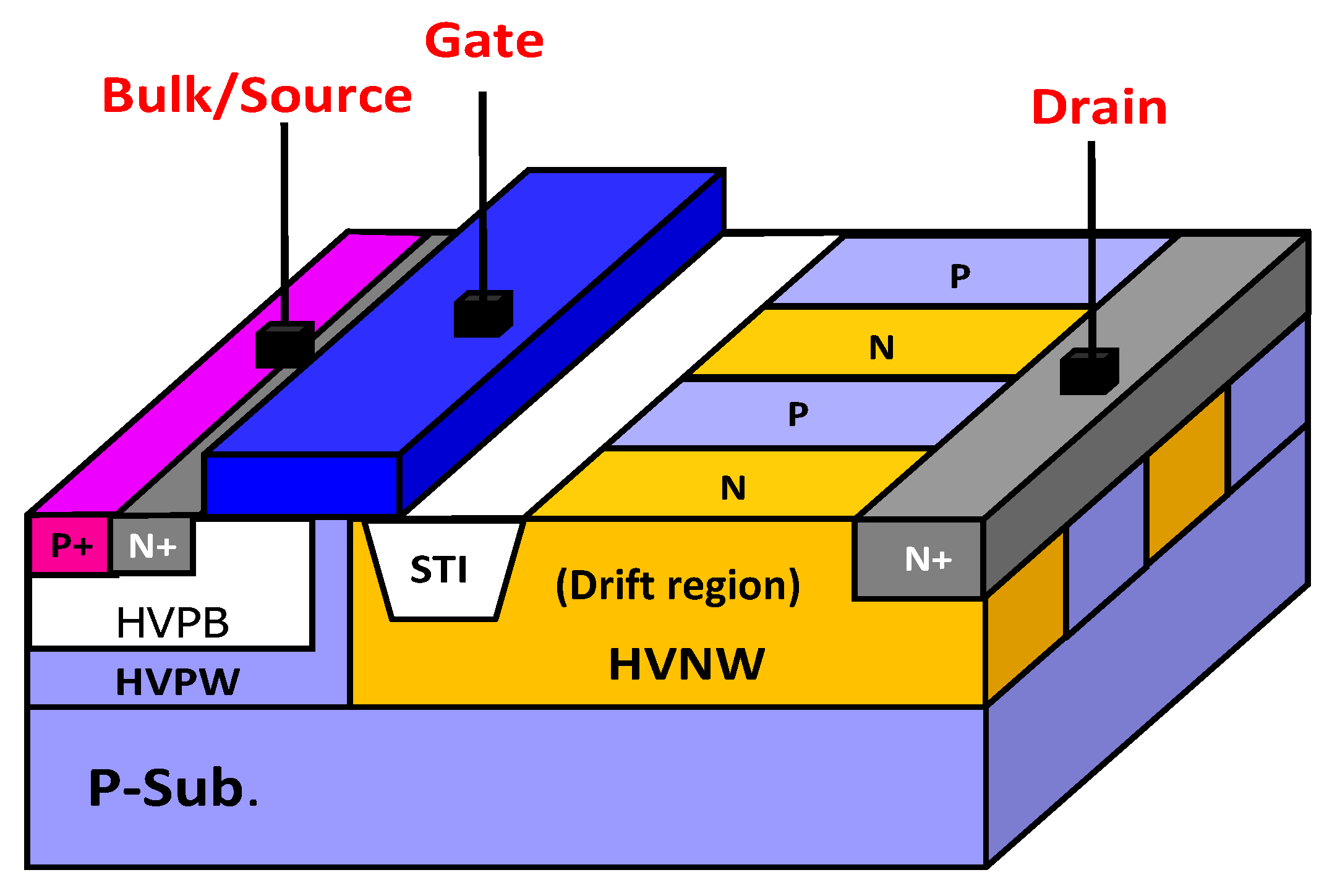
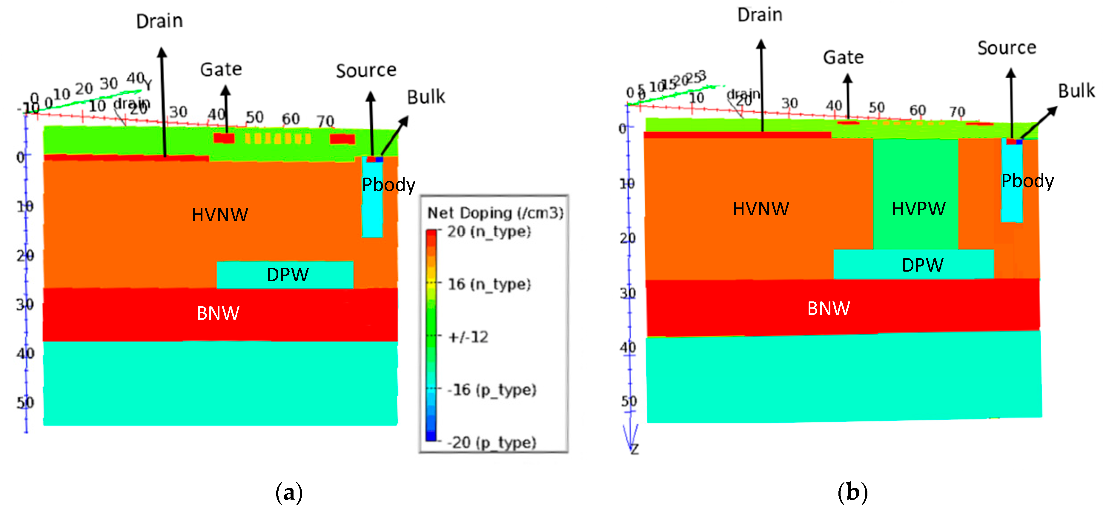
2.1. The Benchmarked Reference Sample (Pure nLDMOS)

The layout diagram and 3-D cross-sectional view (along the line AB of Figure 3a) of a UHV 300 V circular nLDMOS benchmarked reference device are shown in Figure 3a,b, respectively. In Figure 3a, due to the high operation voltage and high breakdown voltage need, a lightly n-doped HVNW layer is used in the drain-side drift region. The PBody and deep P-Well (DPW) layers will form a reduced surface-field (RESURF) structure, which causes the drift region to be completely depleted and increases the breakdown voltage of the device [30]. Similarly, the poly2 surround above the drift region is used to increase the breakdown voltage. In the rectangular-type layout, the current will flow through and concentrate at the electrode corner; therefore this component is easily damaged there. Instead, in Figure 3b, the layout of a UHV MOSFET adopts a circular mode due to the conduction current uniformly flowing along the shortest radial-outward path and a circular structure is used in order to prevent the current’s uneven flowing. Meanwhile, a gate-grounded MOSFET (GGnMOS) structure is commonly used in the routing architecture of an ESD protection device, which discharges the instantaneous current of an external transient pulse mainly through the parasitic bipolar-junction transistor (BJT) conduction of this GGnMOS component. These experimental samples were fabricated by a TSMC 0.5 μm UHV BCD process with a channel length L of 2.5 μm and a channel width W of approximately 394.3 μm.

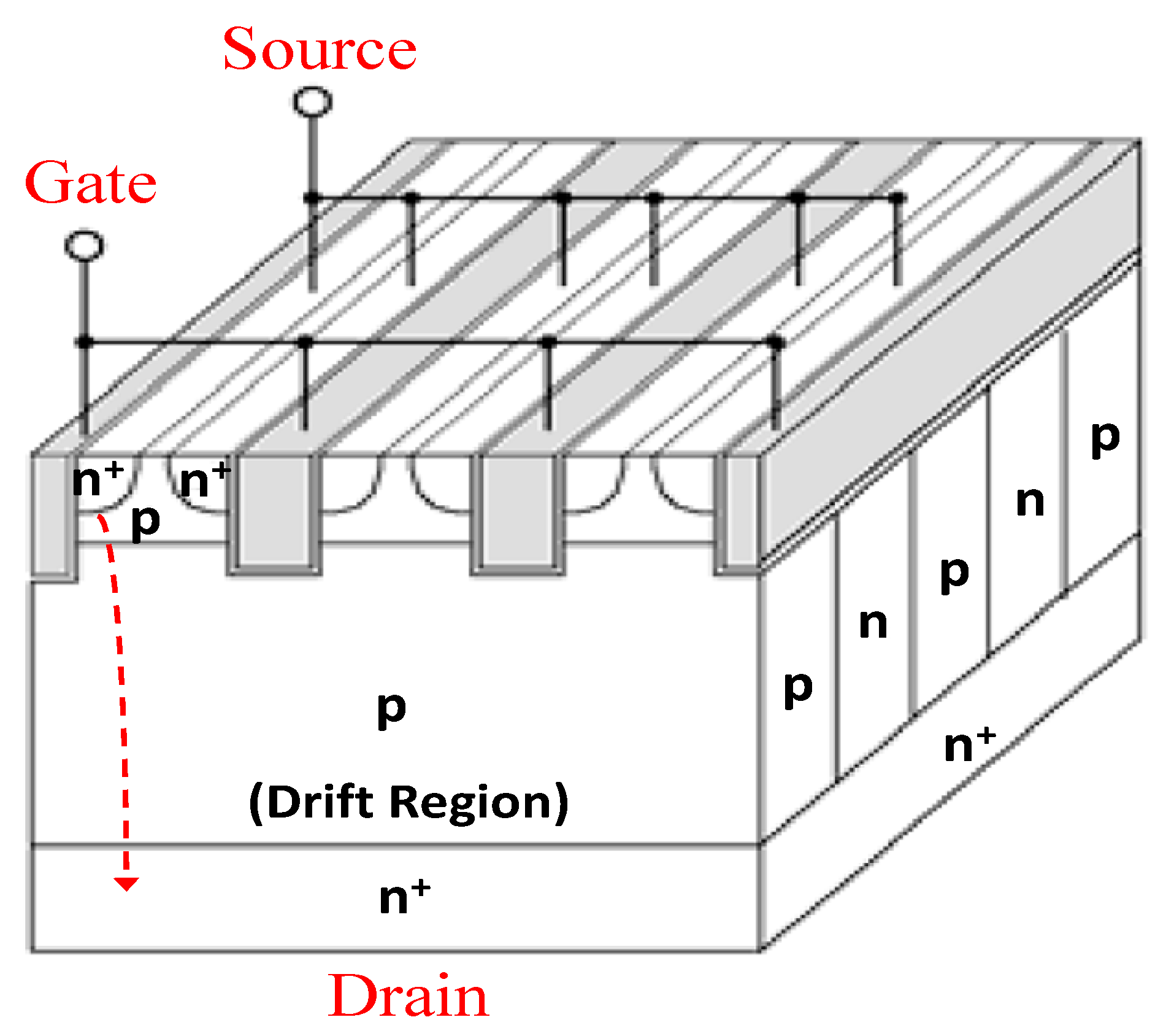
2.2. nLDMOS-SJs Samples with SJs Length Modulation

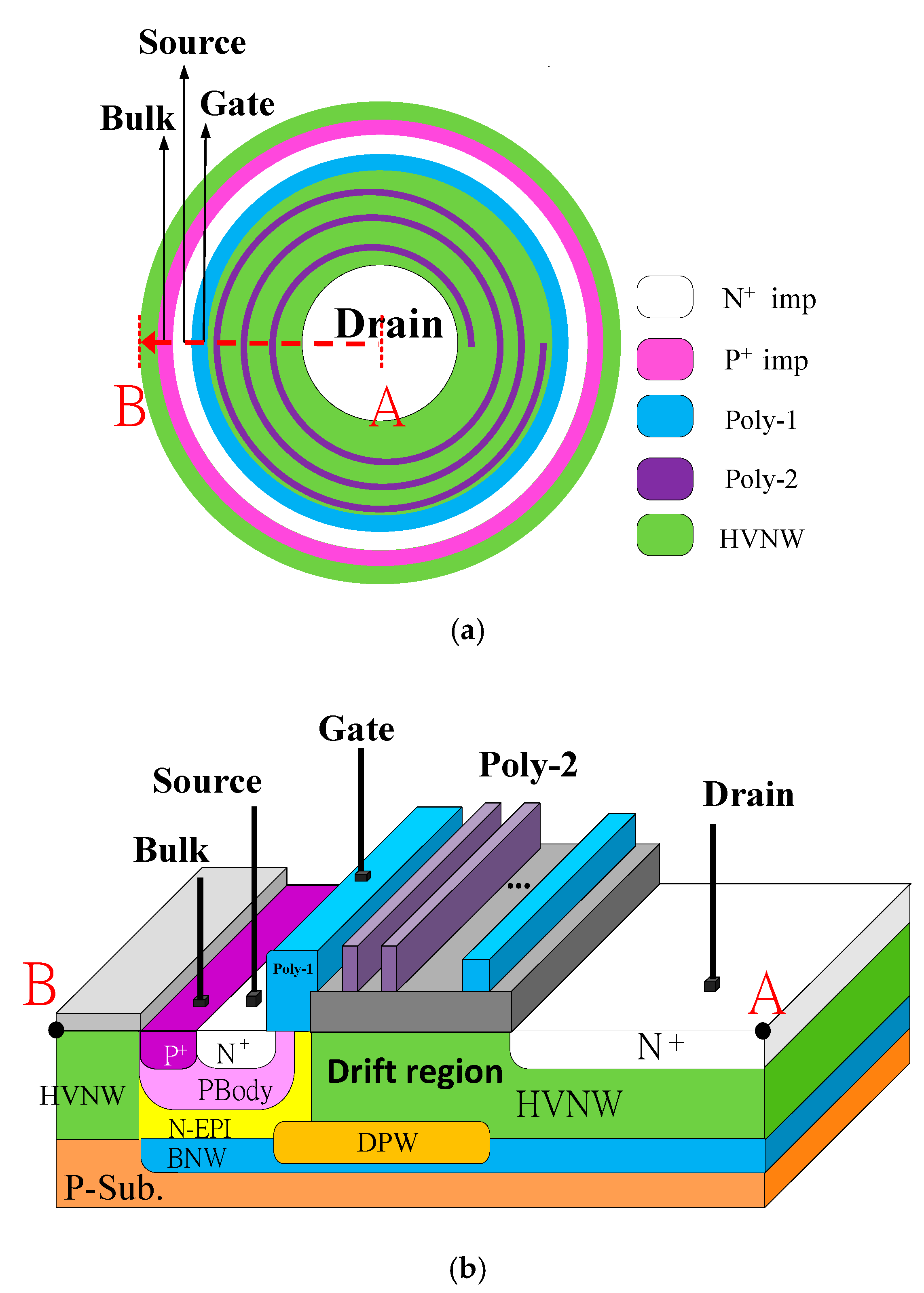
The Symmetrical Eight-Zone Elliptical Cylinder Type (M8) of LDMOS-SJs

Next, the cross-sectional view and layout diagram of a UHV 300 V nLDMOS with symmetrical eight-zone elliptical cylinder SJs (type-M8) in the drain region are presented in Figure 4. This novel arrangement is taken as the length of X (length X) modulation of the HVPW layer embedded in the drain-side drift region. Then, this arrangement is set to increase the length X of the HVPW zone shown in Figure 4b, and which are 5, 10, 15 and 20 μm, respectively. Meanwhile, the width (thickness) of these entire elliptical cylinder SJs are kept to 3 μm. Therefore, this study will mainly discuss the impact of HVPW distribution and how the HBM ability is affected by the HVPW length X.
Based on these devices and the reference sample (previous sub-section) structures, an equivalent circuit of the nLDMOS-SJ devices with SJ length modulation is presented in Figure 5; Rbulk is the parasitic resistances of the source-to-bulk; the BJT is a parasitic device of the gate-grounded nLDMOS device; the parasitic resistance (Rdrift)SJ in the drift region is sufficiently high and varied with the SJs length modulation; and Rdrain is the parasitic resistances of the drain electrode.

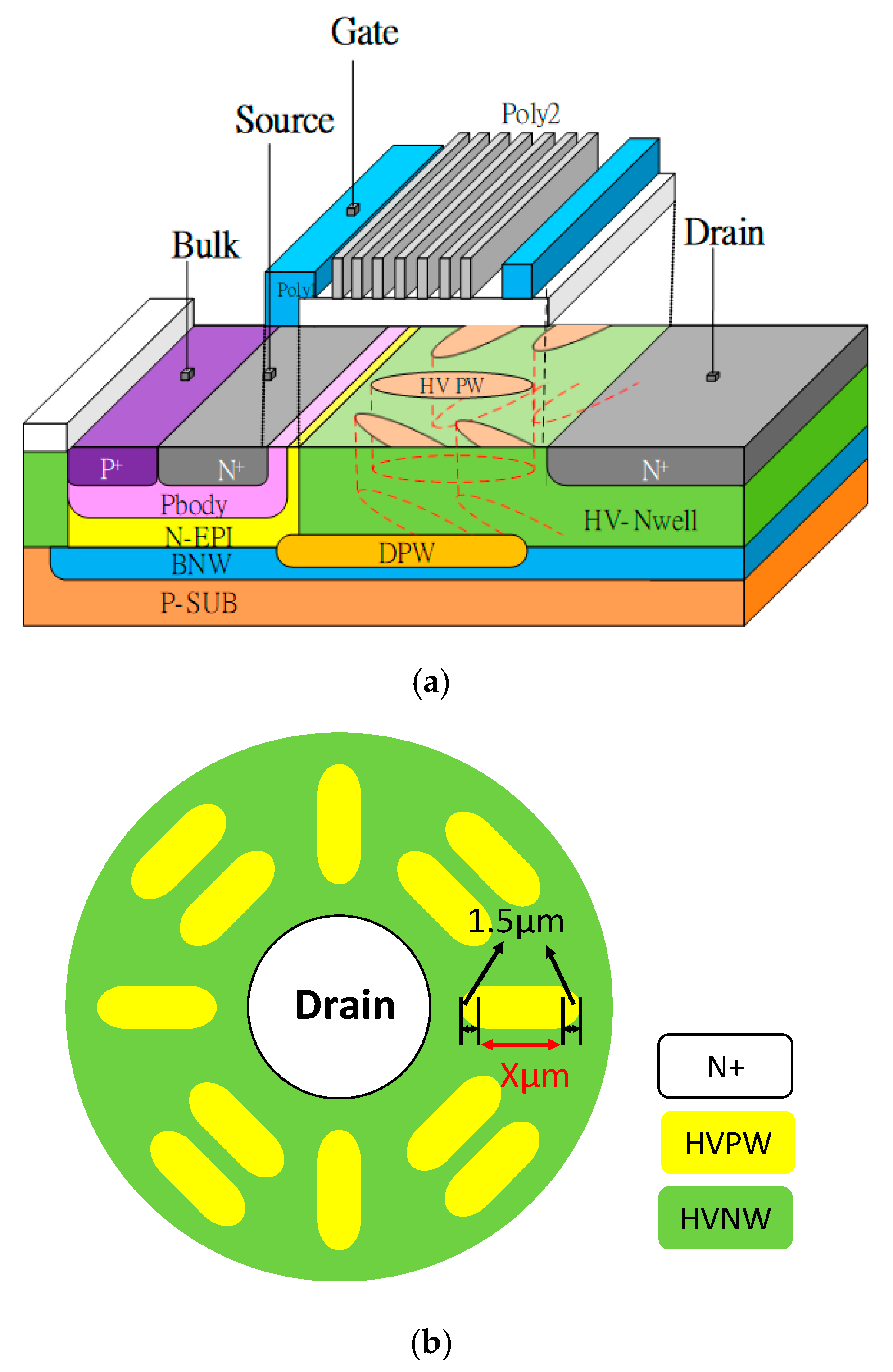
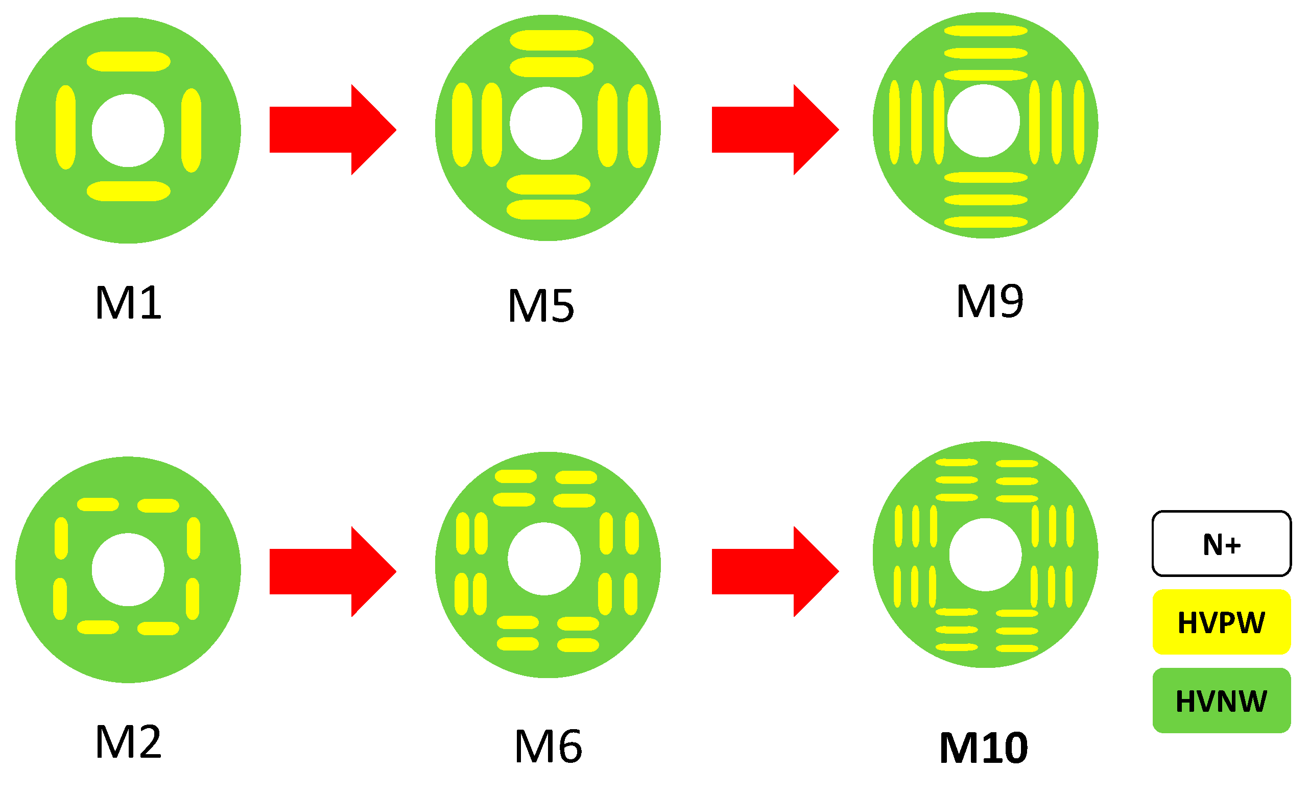
2.3. SJs Number Modulation: Six LDMOS-SJs Devices with the Symmetrical Four-Zone Elliptical Cylinder Type

In Figure 6, the following items are the SJs’ number modulation of symmetrical four-zone elliptical HVPW cylinders, which are classified as the group A (M1, M5, M9) and the group B (M2, M6, M10), respectively. In these six LDMOS-SJ devices, each has a common feature, that is, the SJ on each side is perpendicular to the SJs on the adjacent sides. Additionally the length X of the HVPWs shown in Figure 6 are 20 μm and 5 μm for the group A (M1, M5 and M9) and B (M2, M6 and M10), respectively. Meanwhile, the thicknesses of these six elliptical cylinder SJs are kept to 3 μm. In the case of increasing the HVPWs in this item, we first set the modulation without affecting the breakdown voltage of the electrical characteristics so much, and it is desirable to understand how the modulation impacted on HBM ESD reliability.

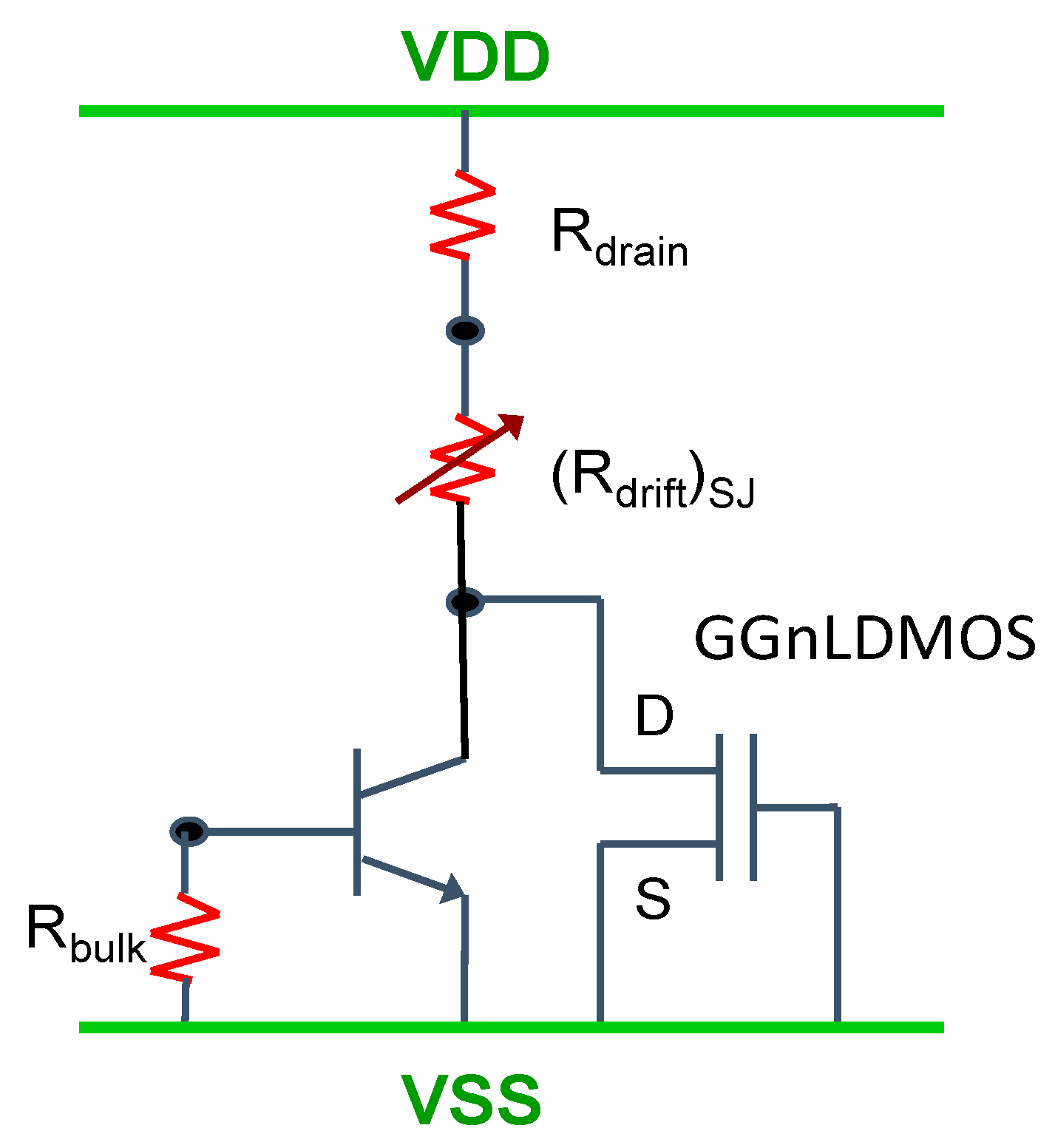
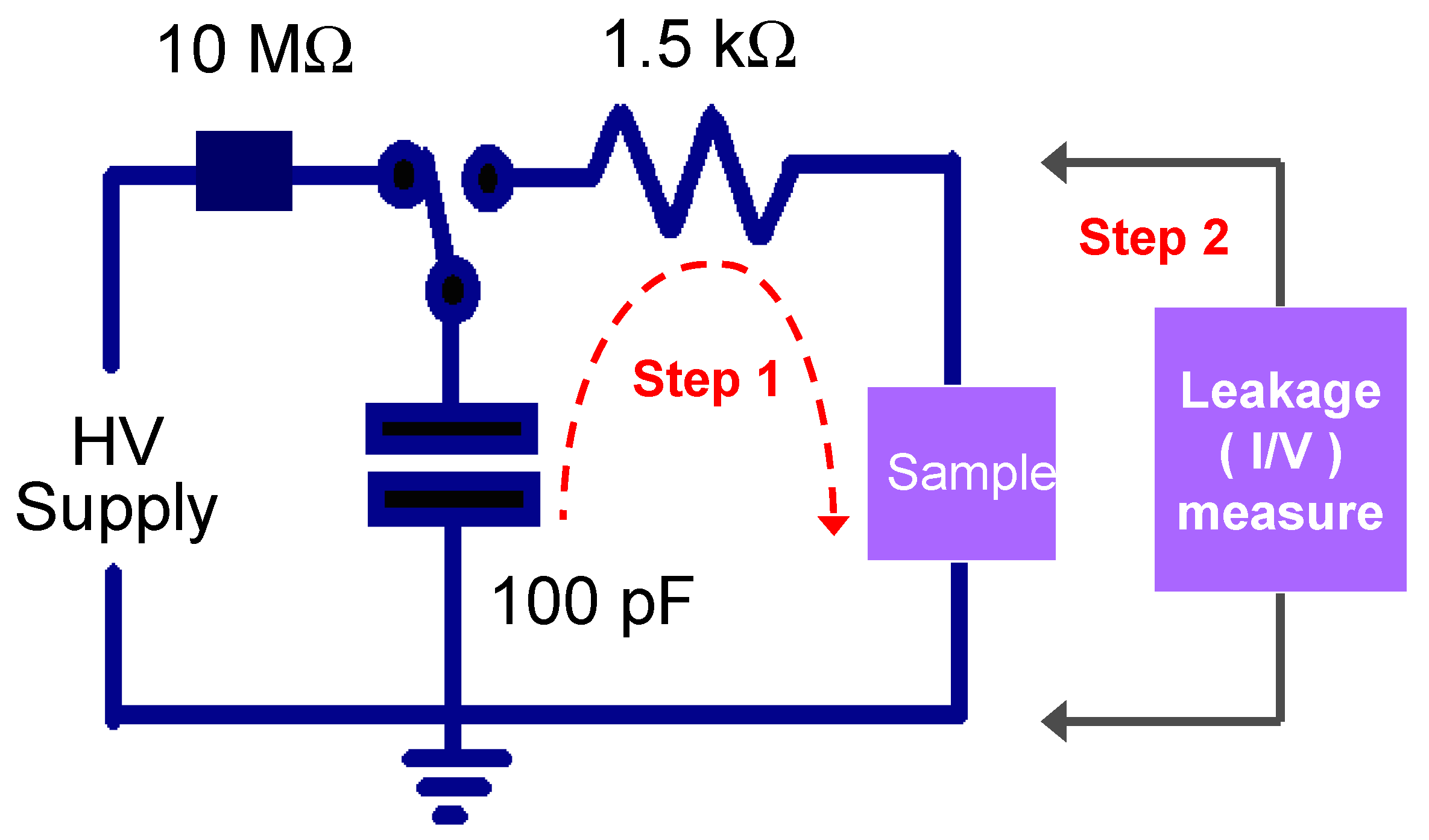
3. HBM Testing System

In the HBM ESD-reliability level testing, a KeyTek MK2 ESD testing machine was used. The ESD testing mode was human-body model (HBM) and the maximum zapping-voltage can be zapped up to ±8000 V. The testing waveforms were confirmed by the MIL-STD-883 EOS/ESD and ANSI/ESDA/JEDEC JS-001 test standards [51,52]. Then, we used the positive-to-VSS (PS) mode (applied a zapping voltage to the drain terminal of this device) for these testing samples. Furthermore, the testing arrangement is shown in Figure 7. The testing voltages for HBM testing were in the range of 500 to 8000 V and changed by 250 V per interval in the step-1 HV zapping. A quantity of I-V curve was selected as the failure judge criterion in the step-2 leakage-current measurement. Therefore, the leakage-current was fixed at 1 μA for sensing before/post HBM zapping and compared for I-V curve variations. If the voltage-shift changed by more than ±30% (ΔVshift > ±30%), then this pin was decided as not qualified at this HBM zapped level.

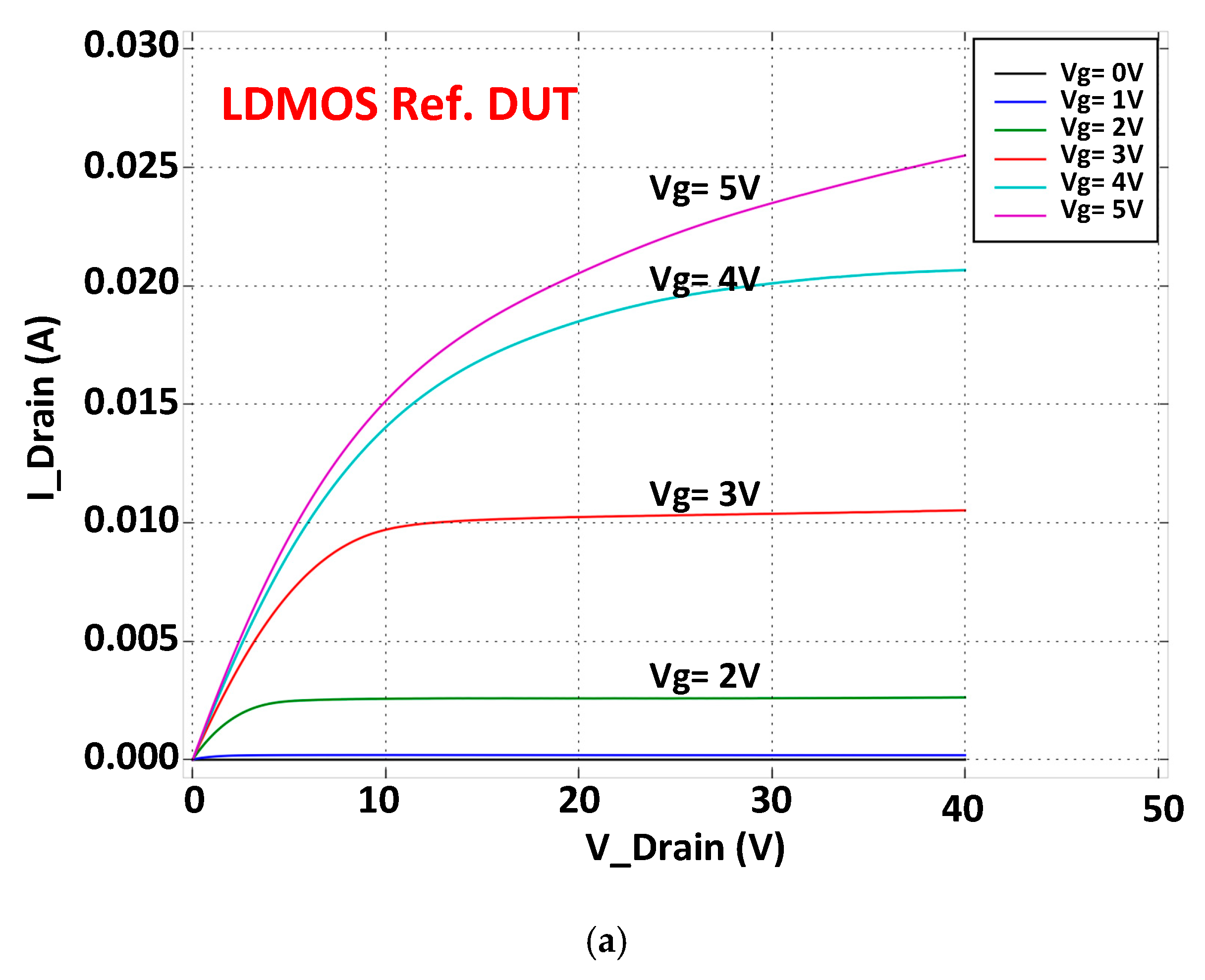
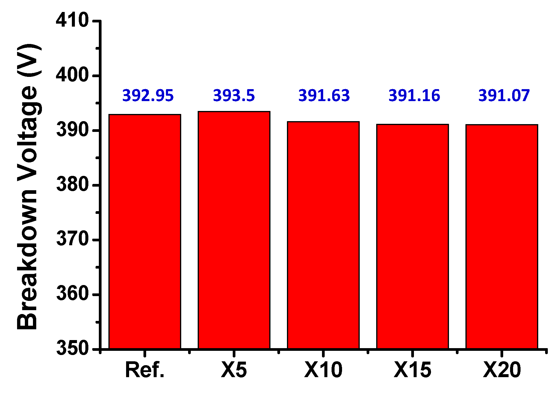
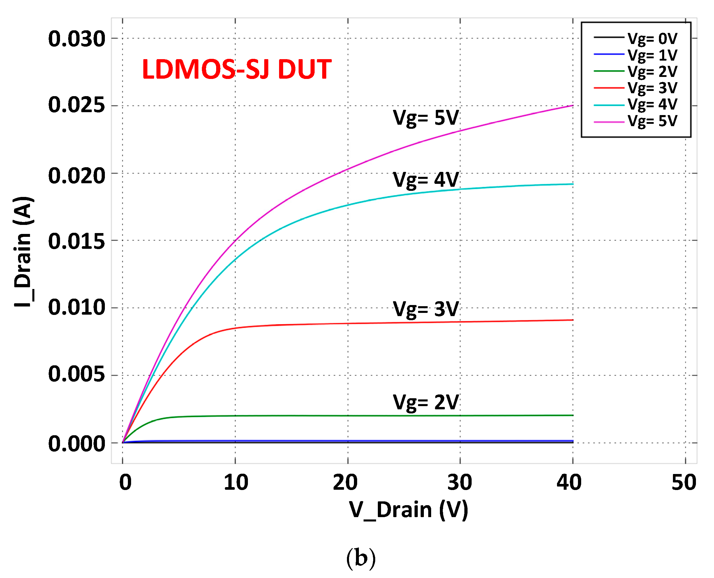
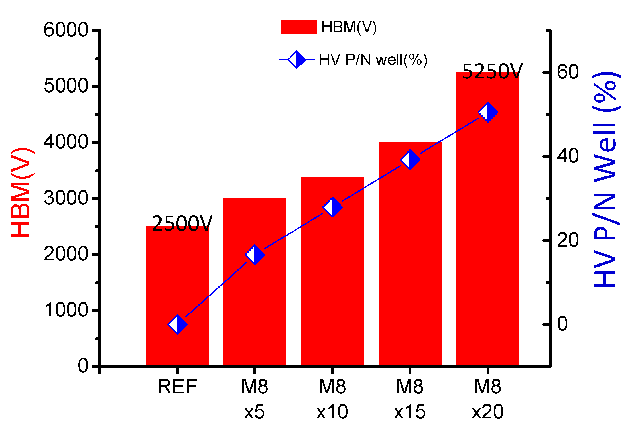
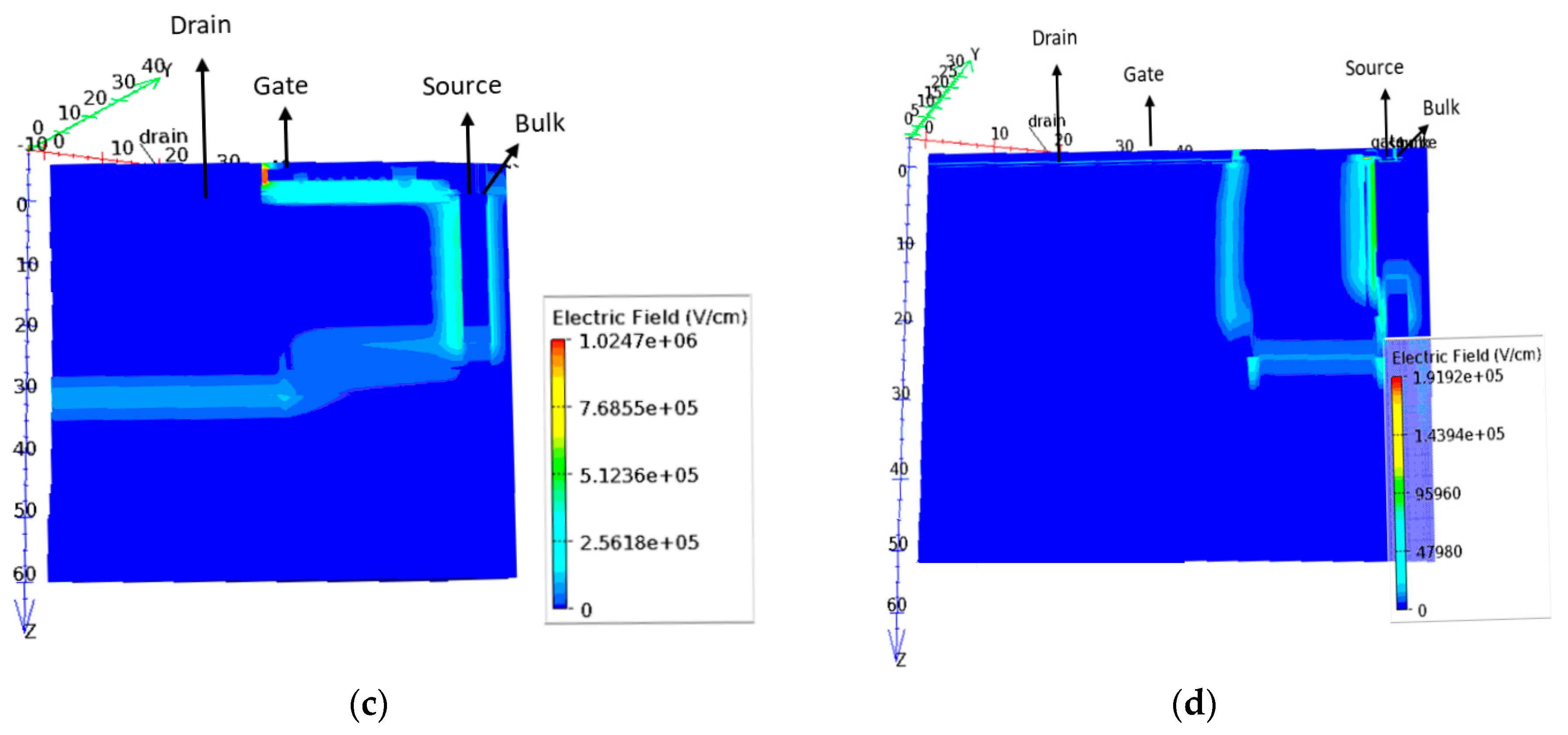
4. Experimental Data and Discussion

Even LDMOSs with the super-junction (SJ) structures were recently developed to obtain the trade-off targets between the breakdown-voltage (VBK) capability and the on-resistance behavior which are always the key issues in the design of power electronics. The SJ architecture is chiefly to gain charge compensation in the off-state (an ESD device with GGnMOS configuration is operated at the normally-off state) of a UHV device, by alternating doped N- and P-pillars comprising the drift region near the device drain side.
Firstly, the experimental results of normal output I-V characteristics of the UHV 300 V reference nLDMOS and nLDMOS-SJs type-M8 with X = 10 μm are shown in Figure 8. Obviously, these output I-V behaviors changed very little after adding elliptical cylinder SJs. For example, Vg = 5 V and Vd = 40 V, and the drain currents were equal to 2.551 mA and 2.5 mA, respectively. The output I-V variation does not exceed 1.88%. Meanwhile, on the other hand, the breakdown voltages of these nLDMOS related devices with symmetrical eight-zone elliptical cylinder SJs in the drain region are presented in Figure 9. From these experimental results, there is not much change in the breakdown-voltage (VBK) test after adding the SJ structure, which fall between 391 and 393.5 V (the original benchmarked device under test (DUT) is 393 V). The VBK‘s value variation does not exceed 0.51%, it means that the basic electrical properties of the nLDMOS components are carefully controlled so that they do not change much. That is, in this study, we want to enhance the ESD-reliability capability without affecting the original electrical behavior afterwards by painstakingly adding these SJ structures.
In Figure 10, the HBM immunity level of the benchmarked GGnLDMOS reference DUT is 2500 V. As the symmetrical eight-zone elliptical cylinder SJs (type-M8) are embedded in the drain-side drift region of the nLDMOS and the length X of the HVPW layer is modulated, it is found that the HBM capability of these nLDMOS-SJ samples increases as the length X of the HVPW layer (also called the HV PW/NW area ratio) becomes longer and larger. When the HVPW length X is 20 μm, the HBM capability value can be promoted up to 5500 V, so its ESD capability is improved by 120% as compared with the original benchmarked GGnLDMOS device. Due to the previous description of the equivalent circuit of Figure 5, an nLDMOS device embedded SJ in the drift region can be equivalently regarded as a variable linear resistor [53]. Therefore, by the linear-regression technique, a strongly linear relationship for the HBM immunity levels of these M8s versus the HVPW/HVNW area ratio can be found in Equation (1),
V H B M = ( V H B M ) 0 + C × ( A r e a R a t i o % ) H V P W / H V N W 2240 V + 5157.1 V × ( A r e a R a t i o % ) H V P W / H V N W
where the (VHBM)0 is the HBM fitting level for the nLDMOS reference sample and C is a linear-proportional slope constant, such as here for these type-M8 samples the (VHBM)0 is 2240 V and C is 5157.1 V, respectively.
By using the Silvaco EDA software for electric field verifications, Figure 11a,b are the 3-D side view diagrams of a thin-slice structure for the nLDMOS reference device and the nLDMOS-SJ M8_X20 device, respectively. Then, a high voltage of 400 V was applied at the drain terminals of these two DUTs for comparing high electric-field distributions. From Figure 11c, the electric field of the circular nLDMOS reference device was concentrated at the depletion area of the LOCOS edge under this high voltage biase, and the peak value of the electric field is about 1.0247 × 10⁶ V/cm. However, in Figure 11d for the nLDMOS-SJ M8_X20 device, the electric field is concentrated between HVPW and N-EPI, and the depletion region by the SJ (HVPW and HVNW). The maximum electric field of the nLDMOS-SJ M8_X20 device is downgraded to approximately 1.9192 × 10⁵ V/cm, and the peak value of this electric field decreases to the ratio of 18.73% compared with the nLDMOS reference device. Obviously, it reveals that the nLDMOS-SJ structure can indeed reduce the peak electric field of the device.
Next, for proof again by the symmetric four-zone elliptical cylinder SJ modulation, the HVPW structures (M1, M5 and M9, and M2, M6 and M10) are embedded in the drain side, and the HBM values are presented in Figure 12. Because they are not as highly symmetrical as the type-M8 devices, the HBM capability versus the HVPW/HVNW area ratio cannot be satisfactorily linearly related, but can be with another high-order proportional relationship for these group A and B samples. Nevertheless, the HBM ESD capability is somewhat higher with the increase in the number of HVPW SJs. The highest HBM value of M5 (4500 V), its (the M5) ESD capability, is improved by 80% as compared with the original benchmarked GGnLDMOS DUT. Meanwhile, it is found that the HVPW/HVNW area ratio of the group A samples is generally higher than that of the corresponding group B devices, so their ESD HBM abilities are also relatively high. In the case of M9 and M10 (three HVPW SJ arrays in the outward direction), HBM values are downgraded than that of the M5 and M6 (two HVPW SJ arrays in the outward direction). This is caused by the thin-oxide definition (OD) distance from the outermost HVPW to the gate and the heat dissipation cross-sectional area being too small, resulting in a decreasing data value in the HBM robustness.

5. Conclusions

This paper is focused on the enhancements of HBM-immunity levels for UHV 300 V nLDMOS devices being added with 1) symmetrical eight-zone elliptical cylinder SJs (type-M8) in the drain region, in which the length Xs of SJs are 5, 10, 15 and 20 μm, respectively; and 2) symmetrical four-zone elliptical cylinder SJs in the drain region. The first part focuses on the symmetrical eight-zone nLDMOS-SJ experimental samples; we can find that the breakdown-voltages of these samples do change a little due to the addition of this SJ structure. The highest test data does not change by more than 0.51% compared to the original benchmarked GGnLDMOS sample, which means that the basic normal electrical characteristics of nLDMOS-SJ components change very little. In addition, the HBM testing values of these samples are optimal for the X20 sample, and it can be upgraded to 5500 V (120% higher than that of the benchmarked DUT). Meanwhile, a strongly linear relationship between the HBM immunity levels versus the HVPW/HVNW area ratio could be found. That is a very useful indicator of how to improve the ESD immunity in UHV nLDMOS transistors. The second part revealed that, for the symmetric four-zone elliptical cylinder SJs in the drain side, the HBM capability is generally higher with the increase in the number of HVPW SJs, with the highest HBM value of M5 (4500 V) improved by 80%. Then, it can be concluded that a UHV nLDMOS device embedded with symmetric elliptical cylinder SJs in the drift region is a good strategy and the HBM capability of these UHV nLDMOS transistors could be effectively improved without changing the basic electrical properties and adding any extra cell area. Therefore, it is a very positive method for the ESD-reliability enhancement in UHV LDMOS components.

Author Contributions

Conceptualization, S.-L.C. and P.-L.W.; Data curation, P.-L.W. and Y.-J.C.; Formal analysis, P.-L.W. and S.-L.C.; Funding acquisition, S.-L.C.; Methodology, S.-L.C. and P.-L.W.; Project administration, P.-L.W. and S.-L.C.; Resources, Y.-J.C.; Supervision, S.-L.C.; Validation, S.-L.C. and P.-L.W.; Visualization, Y.-J.C.; Writing—original draft, S.-L.C.; Writing—review & editing, S.-L.C. All authors have read and agreed to the published version of the manuscript.

Funding

This research received no external funding.

Acknowledgments

In this work, authors would like to thank the Taiwan Semiconductor Research Institute in Taiwan for providing the process information and fabrication platform. Authors would also like to acknowledge the financial support of the Ministry of Science and Technology of Taiwan.

Conflicts of Interest

The authors declare no conflict of interest

Nomenclature

BCDBipolar-CMOS-DMOS
BJTBipolar-junction transistor
BNWBuried N-type well
DPWDeep P-type well
DUTDevice under test
ESDElectrostatic discharge
GGnMOSGate-grounded nMOSFET
nLDMOSN-channel lateral diffused MOSFET
HBMHuman-body model
HVNWHigh-voltage N-type well
HVPBHigh-voltage P-type Base
HVPWHigh-voltage P-type well
ICIntegrated circuit
I/OInput/output
Length XThe length of X (the variable length of elliptical cylinders)
LVLow voltage
MVMedium voltage
N-EPIN-type epitaxy layer
ODThin-oxide definition
PBodyP-type body layer
RESURFReduced surface field
RonOn-resistance
SJSuper junction
STIShallow trench isolation
UHVUltra high-voltage
VbkBreakdown voltage

References

  1. Aoike, N.; Hoshino, M.; Iwabuchi, A. Automotive HID headlamps producing compact electronic ballasts using power ICs. IEEE Ind. Appl. Mag. 2002, 8, 37–41. [Google Scholar] [CrossRef]
  2. Tee, E.K.C.; Julai, N.; Hai, H.Y.; Pal, D.K.; Hua, T.S. Design of 0.18um high voltage LDMOS for automotive application. In Proceedings of the IEEE International Conference on Semiconductor Electronics, Johor Bahru, Malaysia, 27 November 2008; pp. 6–10. [Google Scholar]
  3. DeVincentis, M.; Hollingsworth, G.; Gilliard, R. Long life solid-state RF powered light sources for projection display and general lighting applications. In Proceedings of the IEEE MTT-S International Microwave Symposium Digest, Atlanta, GA, USA, 15–20 June 2008; pp. 1497–1500. [Google Scholar]
  4. Shirai, K.; Yonemura, K.; Watanabe, K.; Kimura, K. Ultra-low on-resistance LDMOS implementation in 0.13µm CD and BiCD process technologies for analog power IC’s. In Proceedings of the 21st International Symposium on Power Semiconductor Devices & ICs (ISPSD), Barcelona, Spain, 14–18 June 2009; pp. 77–79. [Google Scholar]
  5. Wang, Y.; Zhang, D.; Lv, Y.; Gong, D.; Shao, K.; Wang, Z.; He, D.; Cheng, X. A simulation study of SOI RESURF junctions for HV LDMOS (>600V). In Proceedings of the International Workshop on Junction Technology, Shanghai, China, 10–11 May 2010; pp. 1–4. [Google Scholar]
  6. Zhu, J.; Qian, Q.; Sun, W.; Lu, S.; Lin, Y. A novel compact isolated structure for 600V Gate Drive IC. In Proceedings of the IEEE International Conference of Electron Devices and Solid-State Circuits, Tianjin, China, 17–18 November 2011; pp. 1–2. [Google Scholar]
  7. Liu, S.; Sun, W.; Huang, T.; Zhang, C. Novel 200V power devices with large current capability and high reliability by inverted HV-well SOI technology. In Proceedings of the 25th International Symposium on Power Semiconductor Devices & ICs (ISPSD), Kanazawa, Japan, 26–30 May 2013; pp. 115–118. [Google Scholar]
  8. Huang, Y.-J.; Ker, M.-D.; Huang, Y.-J.; Tsai, C.-C.; Jou, Y.-N.; Lin, G.-L. ESD protection design with latchup-free immunity in 120V SOI process. In Proceedings of the IEEE SOI-3D-Subthreshold Microelectronics Technology Unified Conference (S3S), Rohnert Park, CA, USA, 5–8 October 2015; pp. 1–2. [Google Scholar]
  9. Ko, K.; Park, J.; Eum, J.; Lee, K.; Lee, S.; Lee, J. Proposal of 0.13um new structure LDMOS for automotive PMIC. In Proceedings of the 73rd Annual Device Research Conference (DRC), Columbus, OH, USA, 21–24 June 2015; pp. 119–120. [Google Scholar]
  10. Zierak, M.; Feilchenfeld, N.; Li, C.; Letavic, T. Fully-isolated silicon RF LDMOS for high-efficiency mobile power conversion and RF amplification. In Proceedings of the IEEE 27th International Symposium on Power Semiconductor Devices & ICs (ISPSD), Hong Kong, China, 10–14 May 2015; pp. 337–340. [Google Scholar]
  11. Chen, Y.; Chang, C.; Yang, P. A Novel Primary-Side Controlled Universal-Input AC–DC LED Driver Based on a Source-Driving Control Scheme. IEEE Trans. Power Electron. 2015, 30, 4327–4335. [Google Scholar] [CrossRef]
  12. Chang, C.; Jiang, T.; Yang, P.; Xu, Y.; Chen, Y. Adaptive line voltage compensation scheme for a source-driving controlled AC–DC LED driver. IET Circuitsdevices Syst. 2017, 11, 21–28. [Google Scholar] [CrossRef]
  13. Matsuda, J.-I.; Kuwana, A.; Kojima, J.-Y.; Tsukiji, N.; Kobayashi, H. Wide SOA and High Reliability 60-100 V LDMOS Transistors with Low Switching Loss and Low Specific On-Resistance. In Proceedings of the IEEE International Conference on Solid-State and Integrated Circuit Technology (ICSSICT), Qingdao, China, 31 October–3 November 2018; pp. 1–3. [Google Scholar]
  14. Wu, C.-Y.; You, H.-C. Effect of SOI LDMOS Epitaxial Layer Thickness on Breakdown Voltage. In Proceedings of the International Symposium on Computer, Consumer and Control (IS3C), Taichung, Taiwan, 6–8 December 2018; pp. 80–83. [Google Scholar]
  15. Theeuwen, S.J.C.H.; Mollee, H.; Heeres, R.; Van Rijs, F. LDMOS Technology for Power Amplifiers Up to 12 GHz. In Proceedings of the 13th European Microwave Integrated Circuits Conference (EuMIC), Madrid, Spain, 23–25 September 2018; pp. 162–165. [Google Scholar]
  16. Malik, W.A.; Abdulkawi, W.M.; Sheta, A.A.; Alzakari, N.F. A 6 Watts LDMOS Wideband Balanced Power Amplifier. In Proceedings of the 16th International Bhurban Conference on Applied Sciences and Technology (IBCAST), Islamabad, Pakistan, 8–12 January 2019; pp. 1053–1056. [Google Scholar]
  17. van Zwol, J.; van den Berg, A.; Smedes, T. ESD Protection by Keep-On Design for a 550 V Fluorescent Lamp Control IC with Integrated LDMOS Power Stage. In Proceedings of the Electrical Overstress/Electrostatic Discharge Symposium, Orlando, FL, USA, 10–12 September 2002; pp. 270–276. [Google Scholar]
  18. Vashchenko, V.-A.; Gallerano, A.; Shibkov, A. On chip ESD protection of 600V voltage node. In Proceedings of the IEEE 23rd International Symposium on Power Semiconductor Devices and ICs (ISPSD), San Diego, CA, USA, 23–26 May 2011; pp. 128–131. [Google Scholar]
  19. Lee, J.-H.; Kao, T.-C.; Chan, C.-L.; Su, J.-L.; Su, H.-D.; Chang, K.-C. The ESD failure mechanism of ultra-HV 700V LDMOS. In Proceedings of the IEEE 23rd International Symposium on Power Semiconductor Devices and ICs (ISPSD), San Diego, CA, USA, 23–26 May 2011; pp. 188–191. [Google Scholar]
  20. Kanawati, R.; Parvin, A.; Rotshtein, I.; Quon, D.; Yankelevich, A.; Aloni, E.; Eyal, A.; Shapira, S. ESD protection schemes and devices embedded in a 700V integrated power management platform. In Proceedings of the IEEE International Conference on Microwaves Communications, Antennas and Electronics Systems (COMCAS), Tel Aviv, Israel, 7–9 November 2011; pp. 1–4. [Google Scholar]
  21. Tsai, J.-R.; Lee, Y.-M.; Tsai, M.-C.; Sheu, G.; Yang, S.-M. Development of ESD robustness enhancement of a novel 800V LDMOS multiple RESURF with linear P-top rings. In Proceedings of the TENCON 2011—IEEE Region 10 Conference, Bali, Indonesia, 21–24 November 2011; pp. 760–763. [Google Scholar]
  22. Kim, S.-B.; Geum, J.; Kyoung, S.; Sung, M.-Y. On-chip stacked Punchthrough diode design for 900V power MOSFET gate ESD protection. In Proceedings of the 12th IEEE International Conference on Solid-State and Integrated Circuit Technology (ICSICT), Guilin, China, 28–31 October 2014; pp. 1–3. [Google Scholar]
  23. Wu, C.-H.; Lee, J.-H.; Lien, C. A Novel Drain Design for ESD Improvement of UHV-LDMOS. IEEE Trans. Electron Devices 2015, 62, 4135–4138. [Google Scholar] [CrossRef]
  24. Chen, Z.; Salman, A.; Mathur, G.; Boselli, G. Design and optimization on ESD self-protection schemes for 700V LDMOS in high voltage power IC. In Proceedings of the 37th Electrical Overstress/Electrostatic Discharge Symposium (EOS/ESD), Reno, NV, USA, 27 September–2 October 2015; pp. 1–6. [Google Scholar]
  25. Sheu, G.; Li, Y.-H. An innovated 500V UHV ESD self-protection device structure. In Proceedings of the International Conference on Electron Devices and Solid-State Circuits (EDSSC), Hsinchu, Taiwan, 18–20 October 2017; pp. 1–2. [Google Scholar]
  26. Kim, S.; LaFonteese, D.; Zhu, D.; Sridhar, D.S.; Pendharkar, S.; Endoh, H.; Boku, K. A new ESD self-protection structure for 700V high side gate drive IC. In Proceedings of the International Symposium on Power Semiconductor Devices and ICs (ISPSD), Sapporo, Japan, 28 May–1 June 2017; pp. 467–470. [Google Scholar]
  27. Pjenčák, J.; Agam, M.; Šeliga, L.; Yao, T.; Suwhanov, A. Novel approach for NLDMOS performance enhancement by critical electric field engineering. In Proceedings of the IEEE 30th International Symposium on Power Semiconductor Devices and ICs (ISPSD), Chicago, IL, USA, 13–17 May 2018; pp. 307–310. [Google Scholar]
  28. Bandi, L.; Hemanth, A.; Kumar, B.H.; Wijaya, A.C.; Sheu, G. Fully Ion-Implanted 1200V LDMOS with Linear P-Top Technology. In Proceedings of the IEEE International Conference on Consumer Electronics—Taiwan (ICCE-TW), Yilan, Taiwan, 20–22 May 2019; pp. 1–2. [Google Scholar]
  29. Amberetu, M.A.; Salama, C.A.T. 150-V class superjunction power LDMOS transistor switch on SOI. In Proceedings of the 14th International Symposium on Power Semiconductor Devices and ICs (ISPSD), Sante Fe, NM, USA, 7 June 2002; pp. 101–104. [Google Scholar]
  30. Permthammasin, K.; Wachutka, G.; Schmitt, M.; Kapels, H. Performance Analysis of Novel 600V Super-Junction Power LDMOS Transistors with Embedded P-Type Round Pillars. In Proceedings of the International Conference on Simulation of Semiconductor Processes and Devices, Tokyo, Japan, 1–3 September 2005; pp. 179–182. [Google Scholar]
  31. Permthammasin, K.; Wachutka, G.; Schmitt, M.; Kapels, H. New 600V Lateral Superjunction Power MOSFETs Based on Embedded Non-Uniform Column Structure. In Proceedings of the International Conference on Advanced Semiconductor Devices and Microsystems, Smolenice Castle, Slovakia, 16–18 October 2006; pp. 263–266. [Google Scholar]
  32. Park, I.-Y.C.; Salama, C.A.T. Super Junction LDMOS Transistors-Implementing super junction LDMOS transistors to overcome substrate depletion effects. IEEE Circuits Devices Mag. 2006, 22, 10–15. [Google Scholar] [CrossRef]
  33. Duan, B.; Yang, Y.; Zhang, B. New Superjunction LDMOS with N-Type Charges’ Compensation Layer. IEEE Electron Device Lett. 2009, 30, 305–307. [Google Scholar] [CrossRef]
  34. Park, I.-Y.; Choi, Y.-K.; Ko, K.-Y.; Yoon, C.-J.; Kim, Y.-S.; Kim, M.-Y.; Kim, H.-T.; Lim, H.-C.; Kim, N.-J.; Yoo, K.-D. Implementation of buffered Super-Junction LDMOS in a 0.18 um BCD process. In Proceedings of the 21st International Symposium on Power Semiconductor Devices & ICs (ISPSD), Barcelona, Spain, 14–18 June 2009; pp. 192–195. [Google Scholar]
  35. Qiao, M.; Wang, W.-L.; Li, Z.-J.; Zhang, B. Super junction LDMOS technologies for power integrated circuits. In Proceedings of the IEEE 11th International Conference on Solid-State and Integrated Circuit Technology (ICSICT), Xi’an, China, 29 October–1 November 2012; pp. 1–4. [Google Scholar]
  36. Panigrahi, S.K.; Gogineni, U.; Baghini, M.S.; Iravani, F. 120 V super junction LDMOS transistor. In Proceedings of the IEEE International Conference of Electron Devices and Solid-state Circuits (EDSSC), Hong Kong, China, 3–5 June 2013; pp. 1–2. [Google Scholar]
  37. Duan, B.; Yuan, S.; Cao, Z.; Yang, Y. New Superjunction LDMOS with the Complete Charge Compensation by the Electric Field Modulation. IEEE Electron Device Lett. 2014, 35, 1115–1117. [Google Scholar] [CrossRef]
  38. Duan, B.; Cao, Z.; Yuan, S.; Yang, Y. Complete 3D-Reduced Surface Field Superjunction Lateral Double-Diffused MOSFET Breaking Silicon Limit. IEEE Electron Device Lett. 2015, 36, 1348–1350. [Google Scholar] [CrossRef]
  39. Jagannathan, R.; Hoenes, H.-P.; Duggal, T. Impacts of package, layout and freewheeling diode on switching characteristics of Super Junction MOSFET in automotive DC-DC applications. In Proceedings of the IEEE International Conference on Power Electronics, Drives and Energy Systems (PEDES), Kerala, India, 14–17 December 2016; pp. 1–6. [Google Scholar]
  40. Cao, Z.; Duan, B.; Cai, H.; Yuan, S.; Yang, Y. Theoretical Analyses of Complete 3-D Reduced Surface Field LDMOS With Folded-Substrate Breaking Limit of Superjunction LDMOS. IEEE Trans. Electron Devices 2016, 63, 4865–4872. [Google Scholar] [CrossRef]
  41. Zhang, W.; Zhang, B.; Qiao, M.; Li, Z.; Luo, X.; Li, Z. Optimization of Lateral Superjunction Based on the Minimum Specific ON-Resistance. IEEE Trans. Electron Devices 2016, 63, 1984–1990. [Google Scholar] [CrossRef]
  42. Tsai, J.-Y.; Hu, H.-H. New Super-Junction LDMOS Based on Poly-Si Thin-Film Transistors. IEEE J. Electron Devices Soc. 2016, 4, 430–435. [Google Scholar] [CrossRef]
  43. Park, J.; Lee, J.-H. A 650 V Super-Junction MOSFETw ith Novel Hexagonal Structure for Superior Static Performance and High BV Resilience to Charge Imbalance: A TCAD Simulation Study. IEEE Electron Device Lett. 2017, 38, 111–114. [Google Scholar] [CrossRef]
  44. Cao, Z.; Duan, B.; Yuan, S.; Guo, H.; Lv, J.; Shi, T.; Yang, Y. Novel superjunction LDMOS with multi-floating buried layers. In Proceedings of the 29th International Symposium on Power Semiconductor Devices and ICs (ISPSD), Sapporo, Japan, 28 May–1 June 2017; pp. 283–286. [Google Scholar]
  45. Gui, H.; Zhang, Z.; Ren, R.; Chen, R.; Niu, J.; Tolbert, L.M.; Wang, F.; Blalock, B.J.; Costinett, D.J.; Choi, B.B. SiC MOSFET versus Si Super Junction MOSFET-Switching Loss Comparison in Different Switching Cell Configurations. In Proceedings of the IEEE Energy Conversion Congress and Exposition (ECCE), Portland, OR, USA, 23–27 September 2018; pp. 6146–6151. [Google Scholar]
  46. Cheng, J.; Chen, W.; Li, P. Improvement of Deep-Trench LDMOS With Variation Vertical Doping for Charge-Balance Super-Junction. IEEE Trans. Electron Devices 2018, 65, 1404–1410. [Google Scholar] [CrossRef]
  47. Cao, Z.; Duan, B.; Shi, T.; Dong, Z.; Guo, H.; Yang, Y. Theory Analyses of SJ-LDMOS With Multiple Floating Buried Layers Based on Bulk Electric Field Modulation. IEEE Trans. Electron Devices 2018, 65, 2565–2572. [Google Scholar] [CrossRef]
  48. Tang, P.-P.; Wang, Y.; Bao, M.-T.; Luo, X.; Cao, F.; Yu, C.-H. Improving breakdown performance for SOI LDMOS with sidewall field plate. Micro Nano Lett. 2019, 14, 420–423. [Google Scholar] [CrossRef]
  49. Duan, B.; Li, M.; Dong, Z.; Wang, Y.; Yang, Y. New Super-Junction LDMOS Breaking Silicon Limit by Multi-Ring Assisted Depletion Substrate. IEEE Trans. Electron Devices 2019, 66, 4836–4841. [Google Scholar] [CrossRef]
  50. CoolMOS™ SJ MOSFETs Selection Guide; Infineon Technologies: Neubiberg, Germany, 2019; pp. 1–32.
  51. MIL-STD-883K, Method 3015. 2016. Available online: https://infostore.saiglobal.com/en-us/Standards/MIL-STD-883-K-733707_SAIG_MIL_MIL_1702986 (accessed on 5 March 2018).
  52. ANSI/ESDA/JEDEC JS-001. 2017. Available online: https://www.jedec.org/document_search?search_api_views_fulltext=JS-001-2017 (accessed on 21 March 2020).
  53. Quddus, M.-T.; Tu, L.; Ishiguro, T. Drain voltage dependence of on resistance in 700V super junction LDMOS transistor. In Proceedings of the International Symposium on Power Semiconductor Devices & ICs (ISPSD), Kitakyushu, Japan, 24–27 May 2004; pp. 201–204. [Google Scholar]
Figure 1. Vertical DMOS with an SJ (super-junction) structure in the drain side.
Electronics 09 00730 g001
Figure 2. Lateral DMOS with an SJ structure in the drain side.
Electronics 09 00730 g002
Figure 3. (a) Device layout diagrams, and (b) 3-D structure view of the UHV 300 V circular LDMOS ref. device.
Electronics 09 00730 g003
Figure 4. (a) 3-D structure and (b) drain region magnified diagrams of the UHV 300 V LDMOS (type-M8) with symmetrical eight-zone SJs in the drain region.
Electronics 09 00730 g004
Figure 5. An equivalent circuit of a GGnLDMOS device with symmetrical SJs in the drain region.
Electronics 09 00730 g005
Figure 6. Device layout diagrams of six UHV 300 V LDMOSs with symmetrical four-zone SJs in the drain region.
Electronics 09 00730 g006
Figure 7. Testing procedures of an HBM ESD testing for UHV nLDMOS related devices.
Electronics 09 00730 g007
Figure 8. The normal output I-V characteristics of (a) UHV 300 V ref. nLDMOS, and (b) nLDMOS-SJs type-M8 device with X = 10 μm.
Electronics 09 00730 g008aElectronics 09 00730 g008b
Figure 9. VBK values (shown by the corresponding numbers) comparison of the UHV 300 V GGnLDMOS type-M8 devices with different SJs’ length Xs.
Electronics 09 00730 g009
Figure 10. HBM values and SJ (HVPW) area % comparisons of UHV 300 V GGnLDMOSs type-M8 devices with different SJ length Xs.
Electronics 09 00730 g010
Figure 11. (a) 3-D thin-slice structure of the nLDMOS ref. device, (b) 3-D thin-slice structure of the nLDMOS-SJ M8_X20 device, (c) electric field distribution of the nLDMOS ref. device, and (d) electric field distribution of the nLDMOS-SJ M8_X20 device.
Electronics 09 00730 g011aElectronics 09 00730 g011b
Figure 12. HBM values and SJ (HVPW) area % comparison of UHV 300 V GGnLDMOSs with different symmetrical four-zone SJs.
Electronics 09 00730 g012

