Article

Design and Realization of a Bidirectional Full Bridge Converter with Improved Modulation Strategies

1
Department of Engineering, University of Palermo, 90128 Palermo, Italy
2
School of Aerospace Engineering, Sapienza University of Rome, 00138 Rome, Italy
*
Author to whom correspondence should be addressed.
Electronics 2020, 9(5), 724; https://doi.org/10.3390/electronics9050724
Submission received: 8 April 2020 / Revised: 24 April 2020 / Accepted: 26 April 2020 / Published: 28 April 2020
(This article belongs to the Special Issue Industrial Applications of Power Electronics)

Abstract

:
In this paper a Full-Bridge Converter (FBC) for bidirectional power transfer is presented. The proposed FBC is an isolated DC-DC bidirectional converter, connected to a double voltage source—a voltage bus on one side and a Stack of Super-Capacitors (SOSC) on the other side. The control law aims at the regulation either of the bus current (when the load requires power) or of the SOSC current (when the stack requires a recharge). Analysis and design of the proposed FBC are discussed. A Phase Shift Modulation (PSM) scheme is proposed, along with an improved modulation variant for the efficiency optimization, through a proper reduction of the transformer power losses. The realized prototype, compliant with automotive applications, is presented and experimental results are highlighted. The target power level is 2 kW.

1. Introduction

Energy Storage Systems allow the durable collection of electrical energy arising from different sources. With respect to the electrical grid, alternative ways of obtaining power are renewable sources and energy harvesting [1,2,3]. As far as storage systems are concerned, their hybridization is gathering momentum in several fields, such as automotive or aerospace, due to the opportunity to integrate different features in the same storage system. Among the possible electrical storage elements, batteries and supercapacitors offer significant benefits in terms of energy density and power density respectively, so that their combination can lead to improvements in terms of total cost and efficiency [4,5,6,7,8,9]. Investigation of possible power system architectures and power converter topologies in order to properly manage the electrical energy inside a hybrid storage system is therefore an attractive research topic [10,11,12].
According to specific application and power level, different types of power system architectures are possible. A common DC voltage bus is generally used to supply the existing loads and this bus could be either directly connected to a battery or connected to it through a DC-DC converter. The supercapacitor instead shall be properly managed in order to supply the load or to recharge the battery itself—a bidirectional DC-DC converter can be used for this purpose. The mentioned DC-DC bidirectional converter shall be able to control the charge/discharge of the supercapacitor from/to the bus.
State of art and future trends concerning DC-DC converters for automotive applications are widely provided in Reference [13], whereas different investigations on DC-DC bidirectional converters for both supercapacitors and battery charging applications are provided in References [14,15,16,17], with particular focus on reliability, ease of control, sizing and robustness. Due to the potentially high voltage range of a stack of supercapacitors, proper DC-DC converter architectures could be used—in References [18,19,20,21] high-voltage-ratio topologies are described, feasible for several applications such as automotive, DC microgrids and renewable energy sources. At the same time, such high voltage levels could suggest the use of galvanic isolation in order to guarantee safety—in References [22,23,24,25,26,27] different applications of isolated DC-DC converters for energy storage management are reported.
In this paper, an insulated DC-DC bidirectional converter is proposed for the management of a hybrid storage system based on battery and supercapacitor. The proposed topology is a full-bridge converter (FBC), which has been realized and experimentally tested with two DC sources emulating a Stack Of Supercapacitors (SOSC) whose maximum voltage is 70 V and a 28 V bus. The rated power level is 2 kW. In order to avoid expensive clamping networks and maintain a high efficiency target, the conventional Phase Shift Modulation (PSM) has been modified through a novel variant aiming at reducing undesirable voltage spikes.
The proposed power converter could find its application whenever a battery-supercapacitor hybrid storage system is present—the battery provides average power, whereas the supercapacitance is able to provide the peak power pulses. Typical application examples of power system architectures are those inside an Electric Vehicle (EV), based on an automotive DC voltage bus or inside a space launcher, based on an avionic DC voltage bus.
This paper is organized as follows—Section 2 provides a description of the proposed power system architecture and analyzes the proposed bidirectional DC-DC converter; Section 3 focuses on the Full Bridge converter design, accordingly, comparing different modulation strategies; Section 4 reports experimental results concerning a Full Bridge converter prototype, able to transfer a 2 kW power; in Section 5 conclusions are given.

2. Analysis of the Full Bridge Converter (FBC)

The aim of the proposed DC-DC converter is to manage the energy flow between two energy sources, being in the specific case a Stack Of Supercapacitors (SOSC) and a DC voltage bus, as highlighted in Figure 1, showing the power system architecture. A typical current profile, required from the bus section, is highlighted as well: the positive current values correspond to a SOSC discharge, whereas the negative ones correspond to a SOSC recharge. The maximum required current value is 70 A, which is equivalent to a maximum rated power of 2 kW for a nominal DC bus voltage equal to 28 V.

2.1. Energy Sources Model

The SOSC voltage lies in the range 35 V–70 V, whereas the nominal DC bus voltage is 28 V. In Table 1 the SOSC parameters and voltage range are reported, where CSOSC and RSOSC are the SOSC equivalent capacitance and resistance. The reported values arise from the considered specific stack, which is supposed to be a 26s11p (26 series–11 parallel) connection of 2.7 V 10 F 35 mΩ ultracapacitor cells (Maxwell Technologies, San Diego, CA, USA).
Being equal to the product between CSOSC and RSOSC, the SOSC charge/discharge time constant is equivalent to hundreds of ms, so that the SOSC can be considered as a DC power source with respect to a converter switching frequency in the order of tens-of-kHz. For this reason the proposed converter can be analyzed and designed as an actual DC-DC converter.
In Table 2 the DC bus specifications concerning the voltage level are reported.

2.2. Full Bridge Converter Analysis

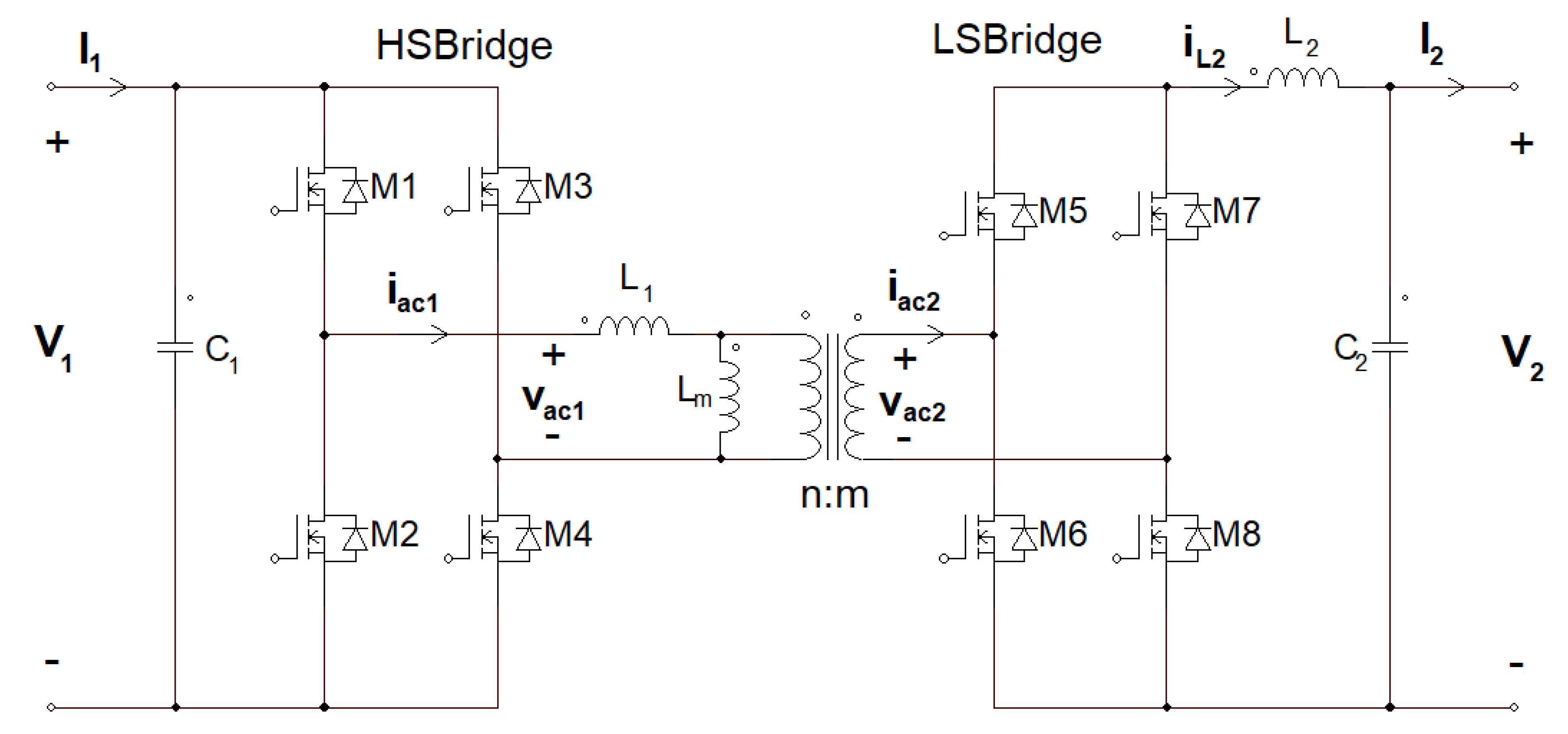
In Figure 2, the schematic of the proposed Full Bridge Converter (FBC) is shown. The FBC is an insulated topology, featuring a transformer between the sections connected to the DC voltages V1 and V2, representing the SOSC and the bus respectively. As far as the transformer is concerned, L1 and Lm are the equivalent primary leakage and magnetizing inductances respectively, whereas n:m is the turns ratio. Each of the H-bridges in the primary and in the secondary side of the transformer consists of four switches, in this specific case four enhancement n-channel MOSFETs—the primary side H-bridge consists of M1-M2-M3-M4, whereas the secondary side one consists of M5-M6-M7-M8. In this network therefore energy can flow in both directions, either from V1 to V2 or from V2 to V1—in the first case the primary H-bridge acts as an inverter and the secondary one as a rectifier, in the second case the H-bridges play the opposite roles.
If a voltage source is connected to V1 port and a load is connected to V2 port, the proposed converter implements a step-down operation.
The primary and secondary H-bridges can therefore be referenced as High-Side Bridge (HSBridge) and Low-Side Bridge (LSBridge).
L2 is the converter inductor, placed in series with the LSBridge.

2.3. Possible Modulation Techniques

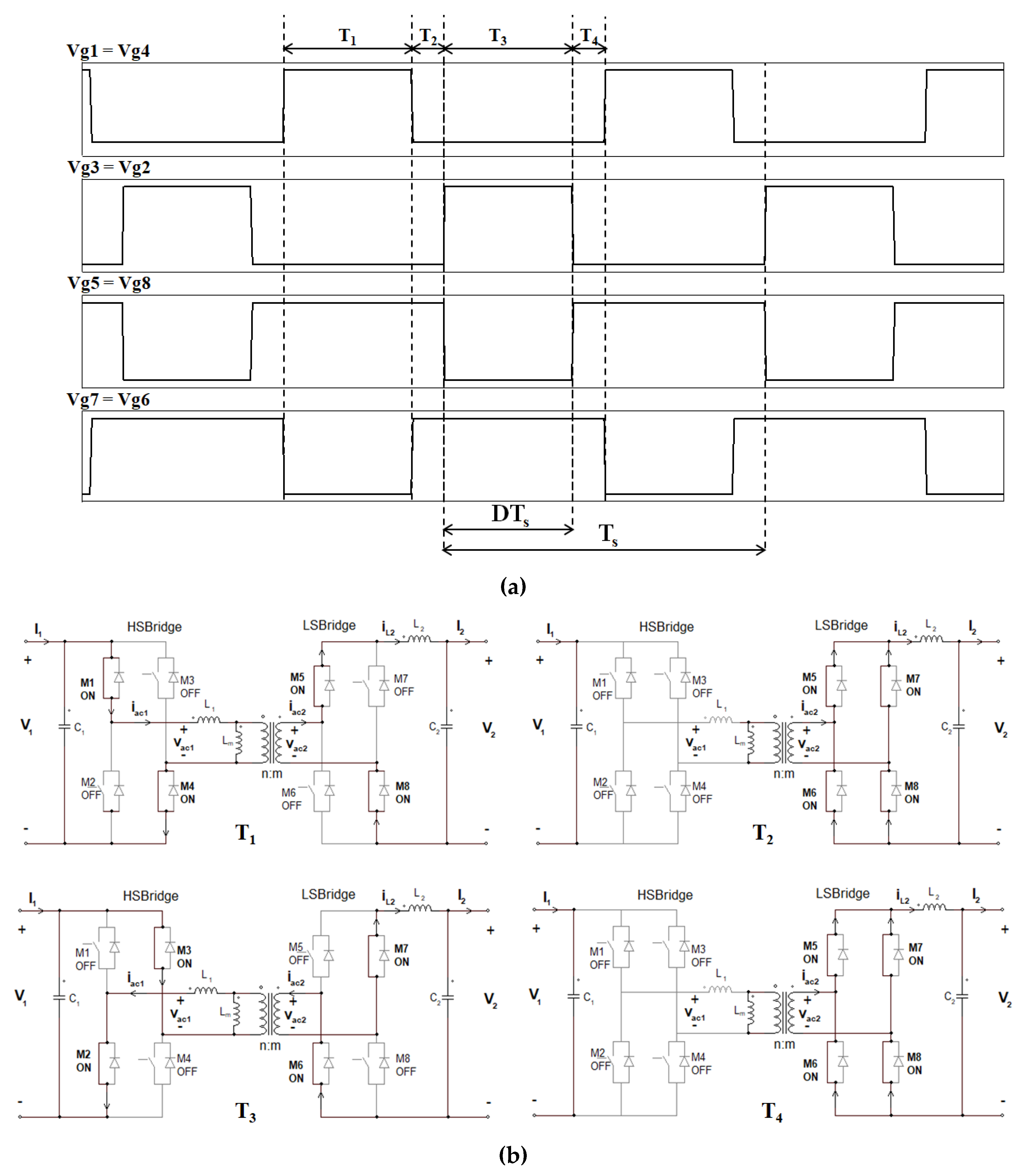
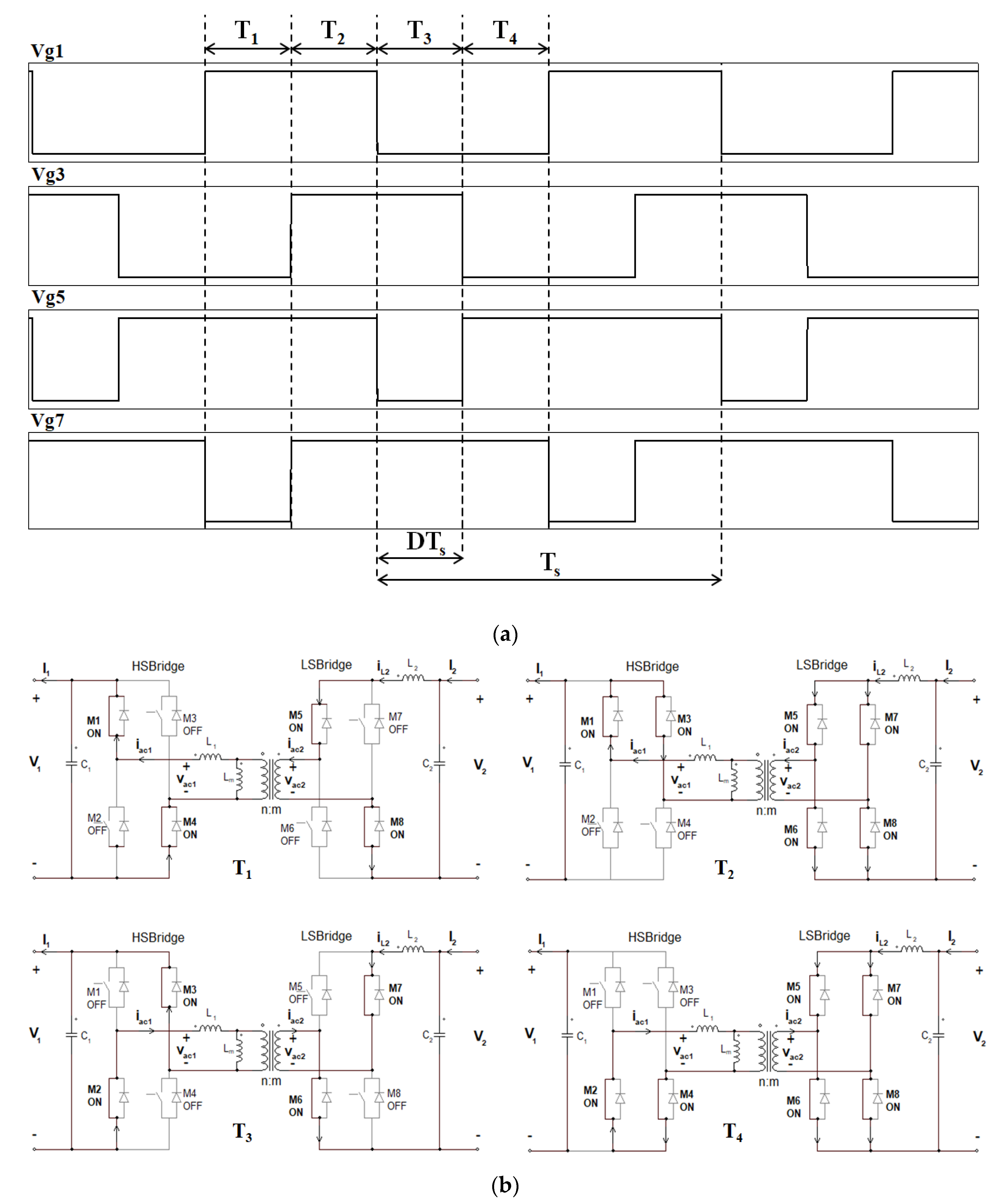
Two possible modulation schemes have been investigated on the proposed FBC, as shown in Figure 3 and Figure 4, Vgn being the logic level applied to the gate-source voltage of the MOSFET Mn—the Pulse Width Modulation (PWM) and the Phase Shift Modulation (PSM).
Figure 3 shows the PWM scheme—M1 and M4 gate signals are in phase, as well as M2 and M3 gate signals and a phase difference occurs between the diagonals M1–M4 and M2–M3; the secondary-side gate signals are obtained by logical negation (NOT) of the primary-side signals, as highlighted in the figure. The on-time of each HSBridge switch is DTs, where D is the duty-cycle and Ts the switching period, being the duty-cycle limited to less than 50% in order to avoid short-circuit at the primary side.
As highlighted by the modes of operation, if D goes higher than 50%, the time windows T2 and T4, corresponding to the L2 discharge towards short circuit, would be deleted, thus avoiding a proper converter working; moreover, the time windows T1 and T3 would be in overlap, thus leading to an undesirable short circuit on V1.
Figure 4 shows the PSM scheme—M1 and M2 are always in phase opposition, as well as M3 and M4; a phase difference, corresponding to the duty-cycle D, occurs between them. The PWM, therefore, is converted into a phase shift modulation.
At the same way as in the PWM, the duty-cycle D is limited to less than 50% in order to avoid open-circuit at the secondary side, which could lead to voltage spikes due to the inductance L2.
As highlighted by the modes of operation, if D goes higher than 50%, the time windows T2 and T4, corresponding to the L2 discharge towards short circuit, would be deleted, thus avoiding a proper converter working, such as in the PWM mode; moreover, the time windows T1 and T3 would be in overlap, thus leading to an undesirable open circuit on L2.
The PSM scheme has been preferred to the PWM, since the PWM scheme involves higher switching power losses, due to the Zero Voltage Switching (ZVS) condition which is reached in the PSM.
The proposed converter aims at the regulation of the power in terms of both amount and direction.
Considering that V1 and V2 are two DC voltage sources—a Stack Of Supercapacitors and a DC bus respectively—the power regulation is therefore consisting in a current regulation.

3. Design and Modulation Strategies for the Proposed Converter

3.1. Choice of the n:m Transformer Ratio

In a conventional full-bridge converter, with a resistive load at its output, the ratio of the output voltage V2 to the input voltage V1 is equal to:
V 2 V 1 = 2 m D n .
This means that for the designed power converter, where voltage sources are applied at both ports (the V1 SOSC source at the input and the V2 bus source at the output), this condition corresponds to a “current balance,” meaning that no DC current is flowing.
In order to produce a current flow, this condition shall be modified. If the SOSC has to discharge into the bus, the duty-cycle, representing the control parameter, shall be increased towards the maximum limit, that is D = 0.5.
The most critical condition is represented by the minimum voltage difference between SOSC and bus, that is when the SOSC is at its minimum voltage (V1 = 35 V) and the bus is at its maximum voltage (V2 = 32 V). In this condition, the V2-to-V1 ratio is at its maximum value, so that, considering that D must be less than 0.5, the secondary-to-primary ratio m:n shall be higher than 1 according to (1), especially considering the case of a positive bus current I2. For this reason, the selected n and m have been chosen according to the following ratio:
n : m = 2 : 3 .
A higher-than-1 turns ratio is even more required considering the voltage drop in the primary side, due to the RSOSC, possibly leading the voltage V1 from 35 V to less than 32 V and all the voltage drops concerning the different components.
If the leakage inductance effect is neglected, the L2 average current IL2,av, corresponding to the bus current, is the following:
I L 2 , a v = 2 m n D V 1 V 2 R e q + ( 2 m n D ) 2 R b o s c = I 2 ,
where Req refers to all the resistive losses in the converter.

3.2. Modulation Strategies

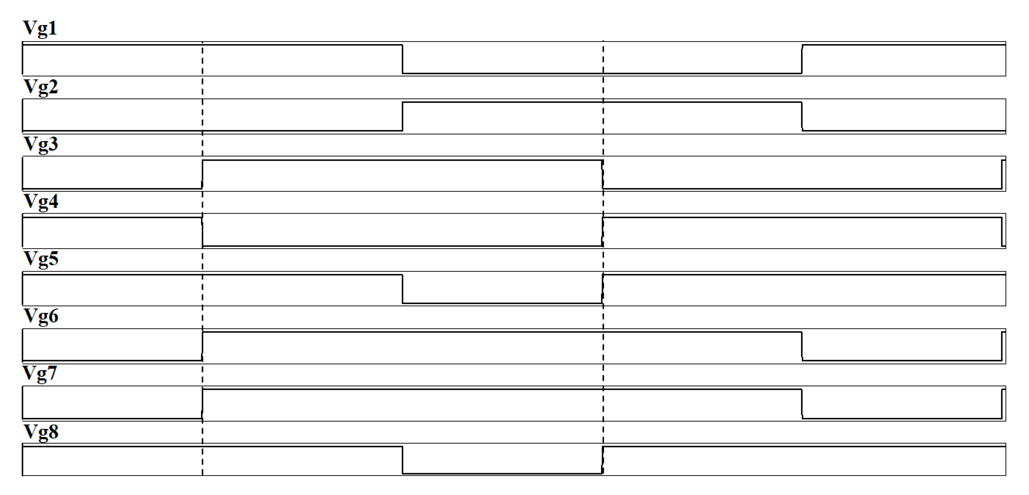
In Figure 5, all the eight gate signals in the case of the previously described Phase Shift Modulation (PSM) are shown in simulation.
As expected by the modulation law and highlighted by the figure, each LSbridge gate signal event is simultaneous with an HSbridge gate signal event.
In Figure 6, the resulting secondary-side waveforms are highlighted, where VL2 is the voltage at the output of the LSbridge and Ts is the switching period.
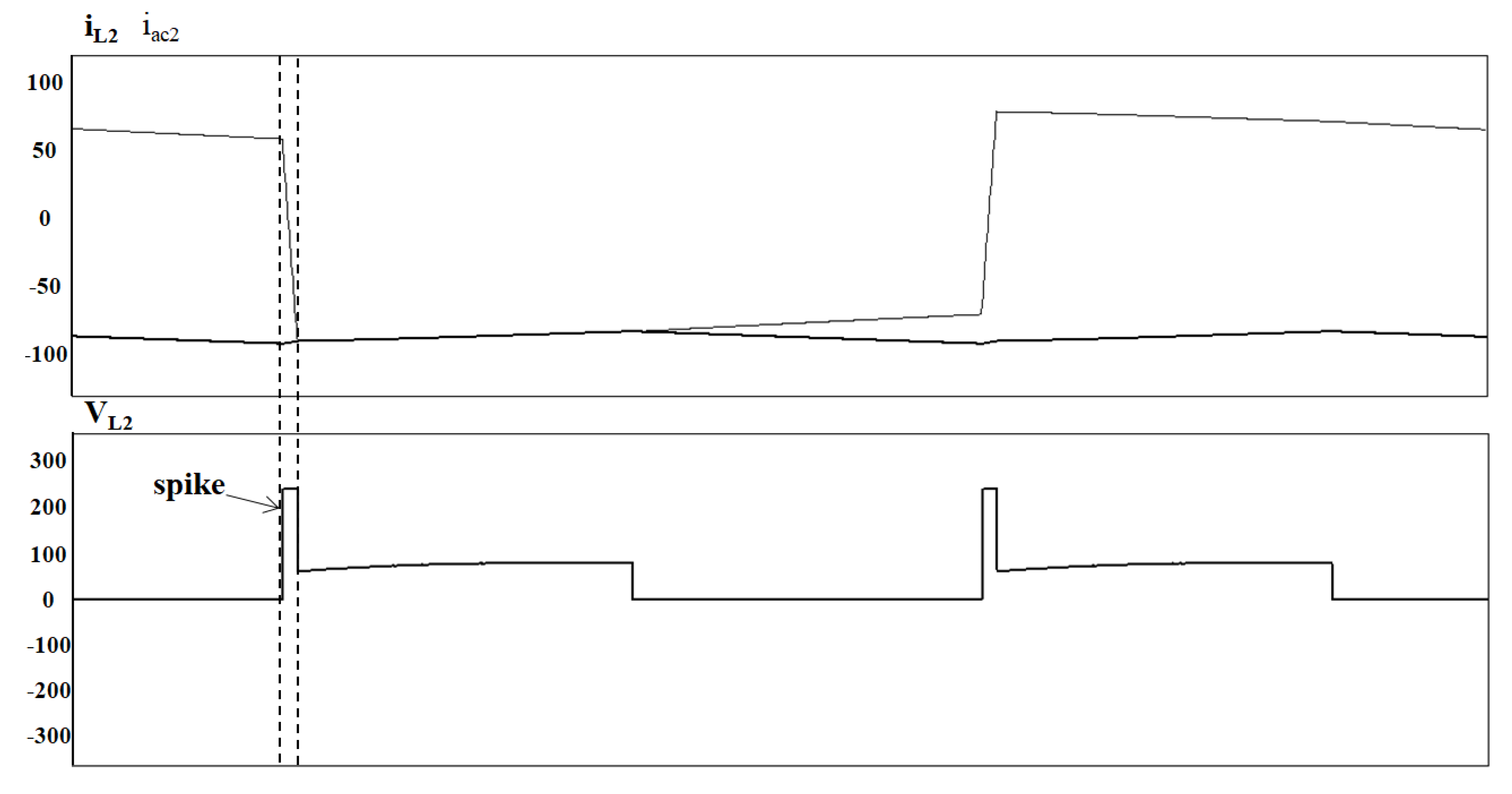
The considered case concerns the SOSC recharge, that is when I2 is negative and IL2,av as well. In this case, IL2 is divided into the drain-source currents of M5 and M7. Every Ts/2, whenever Vg5–Vg8 or Vg6–Vg7 goes low, that is when M5 or M7 is opened, there is no conduction path through the opened MOSFET, due to the reverse direction of the MOSFET-connected diode. Therefore, if before the switch opening the drain-source current on the other switch was negative, a voltage spike on VL2 is provoked since the inductor energy is not free to circulate. This is better highlighted in Figure 7.
A useless energy waste is therefore shown in case of energy flow from V2 to V1 with the conventional PSM.
In order to avoid the mentioned voltage spikes, thus avoiding to limit the overall power system efficiency or to add an expensive clamping network, an improved modulation strategy is proposed in the following.
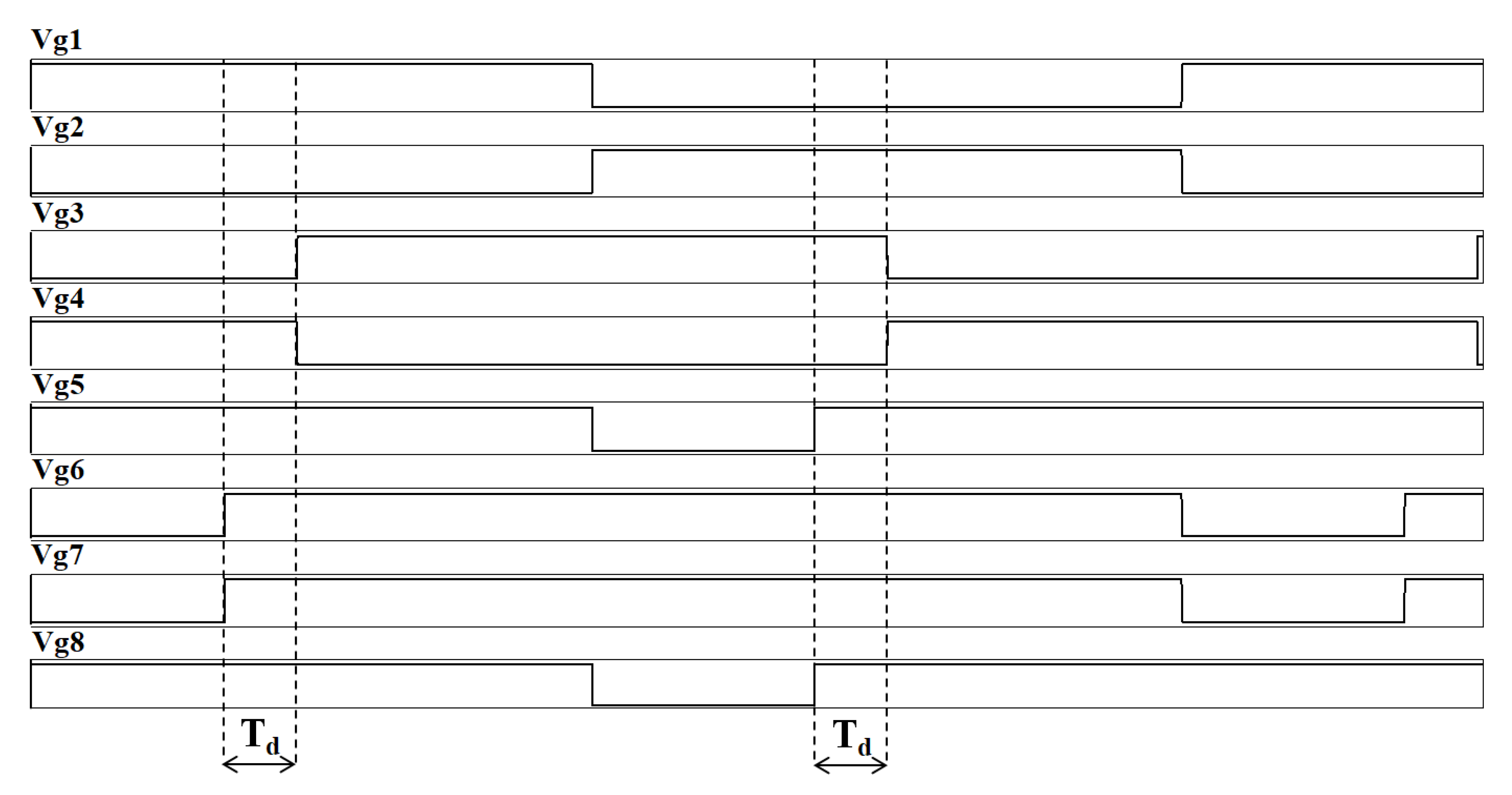
In Figure 8 the gate signals concerning the proposed modified Phase Shift Modulation (PSM) are shown in simulation.
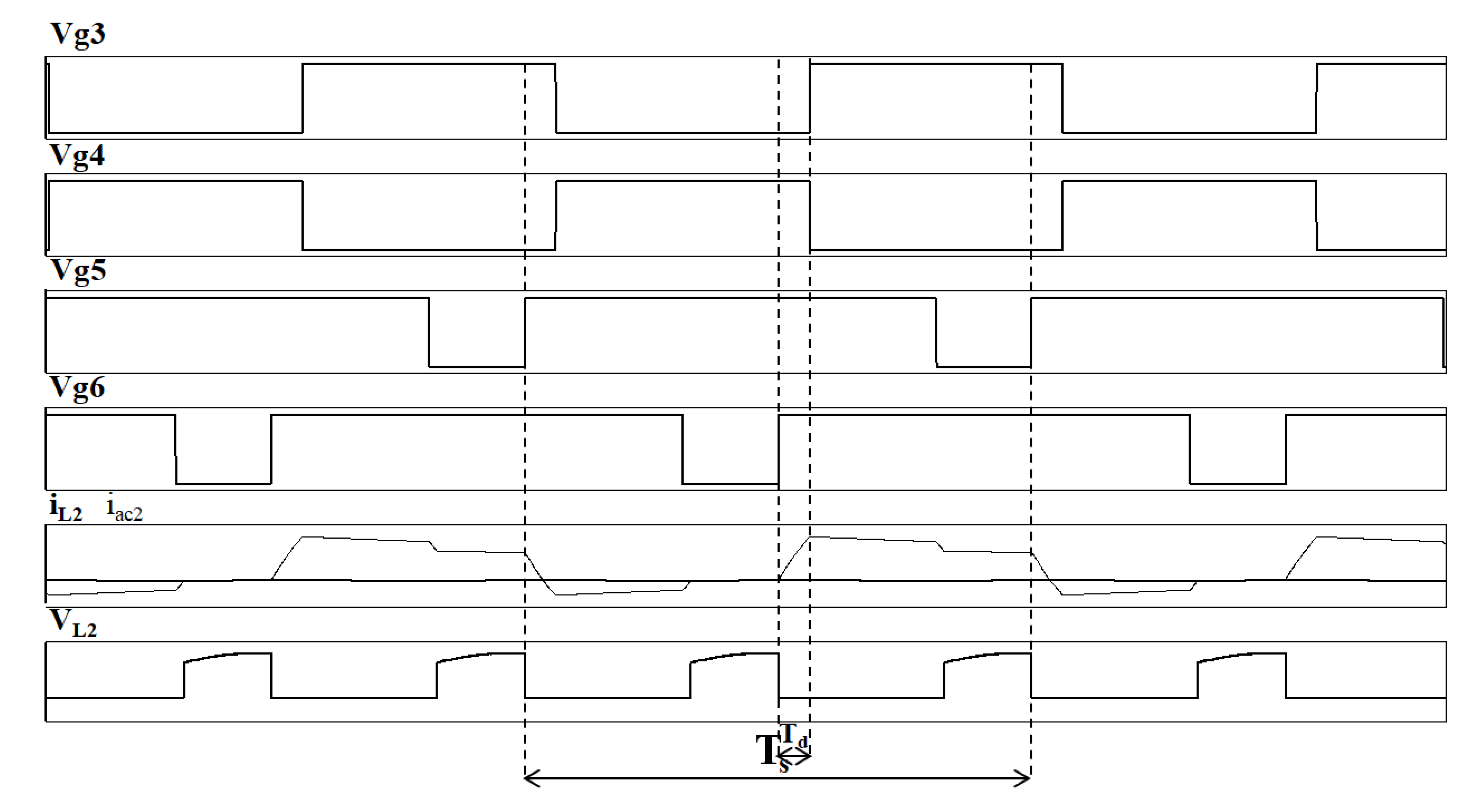
The aim of the improved control law is to open M5–M8 (M6–M7) when the drain-source current on M6–M7 (M5–M8) is positive (negative), that is when iac2 is positive (negative). In order to reach this goal, the positive events of Vgn concerning the LSbridge are anticipated by a time window, referenced as Td, so that iac2 has the time to reverse its sign.
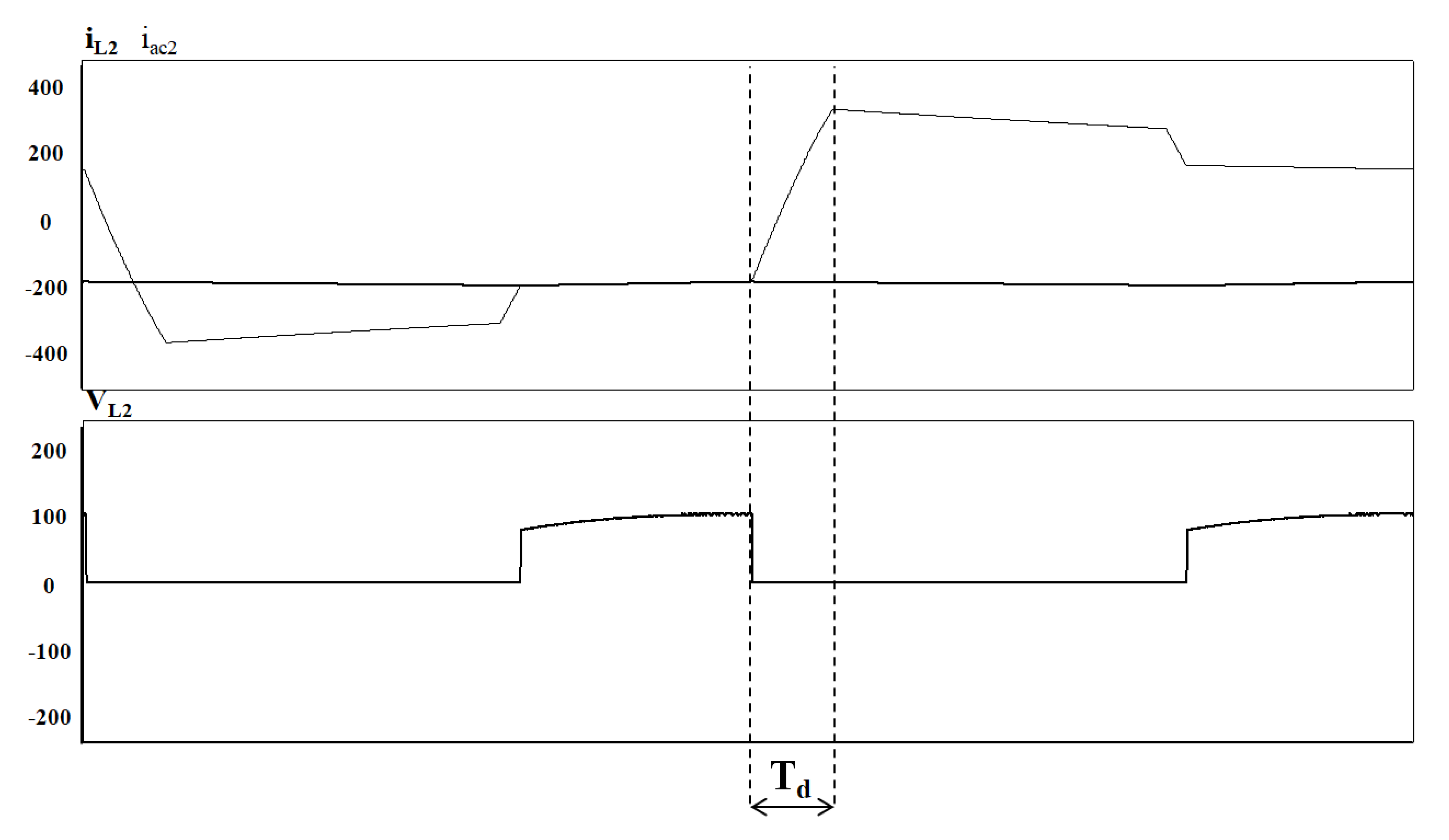
In Figure 9, the resulting secondary-side waveforms are highlighted—this time VL2 presents the ideal shape, as better highlighted by Figure 10.
A power efficiency increase is therefore achievable by means of this improved modulation strategy in case of SOSC recharge, as highlighted in Table 3, reporting system efficiency η for conventional and improved PSM, with respect to the extreme values of V1 and V2, at full power.

4. Experimental Tests

A FBC has been realized aiming at a 2 kW power target and compliant with the specifications concerning the DC voltage sources and the current requirements. The mounted converter consists of the following parts—the power board, including the actual FBC, filtering networks, protection switches and transducers for telemetries; a control board, including signal conditioning, input/output interfaces, controller and gate signals generation; an auxiliary power supply, including power converters to generate all internal supply lines; a mechanical frame/heatsink for thermal dissipation. The control loop aims at the regulation of the bus current value according to its desired value and it has been entirely implemented through analog components.
In Figure 11 the prototypal breadboard is shown. Auxiliary power supply board and control board on the bottom-left corner and bottom-right position can be noted.

4.1. H-bridges Realization

Each power switch in the power board consists of four parallel MOSFETs. The selected components are compliant with Automotive applications and show a TO-247 package. Though-hole type was found convenient as it natively provides connection to multiple PCB layers. In the SOSC-side, AUIRFP4568 nMOSFETs have been used, rated for a maximum 171 A drain current Id,max and for a maximum 150 V source-to-drain voltage VDSS, with a maximum 5.9 mΩ on resistance; in the bus-side, IXFH140N20 × 3 nMSOFETs have been used, rated for a maximum 140 A drain current Id,max and for a maximum 200 V source-to-drain voltage VDSS, with a maximum 9.6 mΩ on resistance.
The bus-side switches have been selected with a higher maximum voltage due to the transformer ratio of the secondary side (bus-side) turns to the primary side (SOSC-side) turns, which is higher than one.
All MOSFETs are driven by means of isolated gate drivers, useful to maintain galvanic insulation between controller and power circuits. The selected component is UCC21521, providing dual independent channels, useful for managing the low-side and the high-side MOSFETs and guaranteeing a 4–6 A (source/sink) current capability and a 16 ns time rise on a 2 nF load capacitance.

4.2. Reactive Components Realization

As far as the used capacitors are concerned, Multi-Layer Ceramic Capacitances (MLCC) are preferred to provide the highest frequency current peaks, since MLCC present equivalent impedances with higher cut frequencies with respect to the electrolytic and Metallized Polyester (PET) ones, which instead contribute to the rms component of the pulsed currents.
The magnetic components with pulsed currents in the tens of A range (the converter inductor L2 and the transformer) have been implemented with EE-type-cores. For the transformer, two magnetic structures have been used, as highlighted by the figure. Copper foils have been used for the windings and multiple wires for the connections with the PCB, in order to have a large current capability. The material used for the transformer cores is 3C95, a power ferrite with high saturation levels and low losses. For L2 a powder core with distributed air gap is used, whose material is Kool Mμ® 40 from (Magnetics, Phoenix, AZ, USA).
In Table 4 and Table 5 the main characteristics of the designed and realized transformer and L2 are respectively reported.
In Table 6, the values of the selected converter switching frequency fsw and reactive components are reported.
For filtering inductors, with DC currents and small ripple, toroidal powder cores are used, with multi-wire windings. The used toroidal core materials are MolyPermalloy Powder (MPP) and High Flux (Magnetics, Phoenix, AZ, USA).
The choice of Lm is based on specifications concerning the desired magnetizing current, whereas the reactive elements selection is based on specifications concerning the desired current ripple at the input and output sections. Details regarding these specifications are beyond the purpose of this paper.

4.3. Experimental Setup

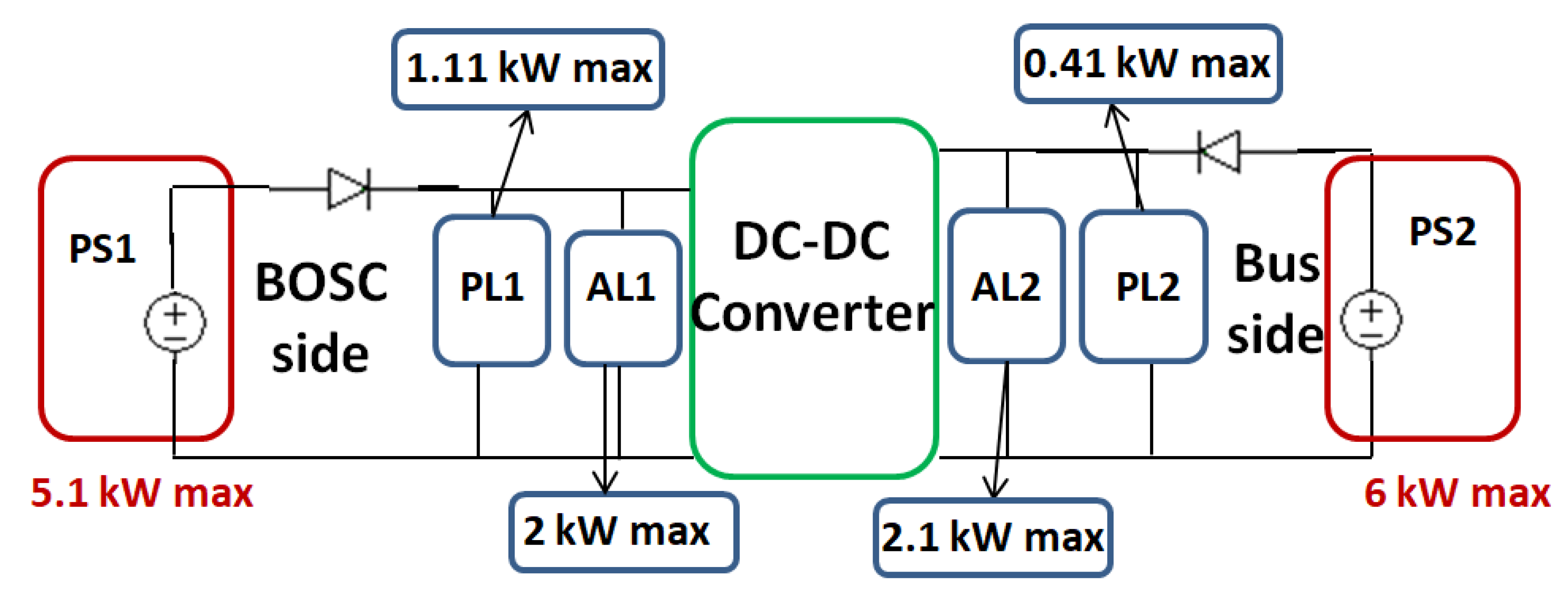
A schematic of the test setup, proposed for full power (2 kW) transfer, is shown in Figure 12.
Each side (SOSC or bus) is emulated by a 1Q (One Quadrant) Power Supply Stack—PS1 and PS2 for SOSC and bus respectively—and a Load Stack, so that a bi-directional power flow can be tested—when the power flows from the SOSC to the bus, PS1 provides the required energy to the bus-side Load Stack; when the power flows from the bus to the SOSC, the SOSC-side Load Stack adsorbs energy arising from PS2.
In order to avoid a negative current flowing through the power supplies, a protection diode is used between the supply and the load. Therefore, 2 protection diodes are used, one on the SOSC side and one on the bus side. Each of them is able to withstand a maximum 200 A current, considering that a maximum 70 A current is supposed to flow in the converter and a maximum 80 A current is needed to continuously supply the Passive Loads. Therefore, in order to guarantee that both the protection diodes are continuously polarized in direct way, a minimum direct current (supposed to be equal to 5 A) shall flow through each of them. Some Passive Loads are needed for this purpose, in order to guarantee the required power absorption.

4.3.1. SOSC-Side Setup

The goal of the SOSC test setup is to guarantee—(35 V–70 V) voltage range; (−2 kW–+2 kW) power range. The SOSC-side Power Supply (PS1) Stack can provide a total maximum power of 5.1 kW. The SOSC-side Load Stack consists of an Active Load (AL1) and a Passive Load (PL1), for a total maximum power of 3.11 kW.

4.3.2. Bus-Side Setup

The goal of the bus test setup is to guarantee—(24 V–32 V) voltage range; (−2 kW–+2 kW) power range. The bus-side Power Supply (PS2) Stack can provide a total maximum power of 6 kW. The bus-side Load Stack consists of an Active Load (AL2) and a Passive Load (PL2), for a total maximum power of 2.51 kW.

4.4. Experimental Results

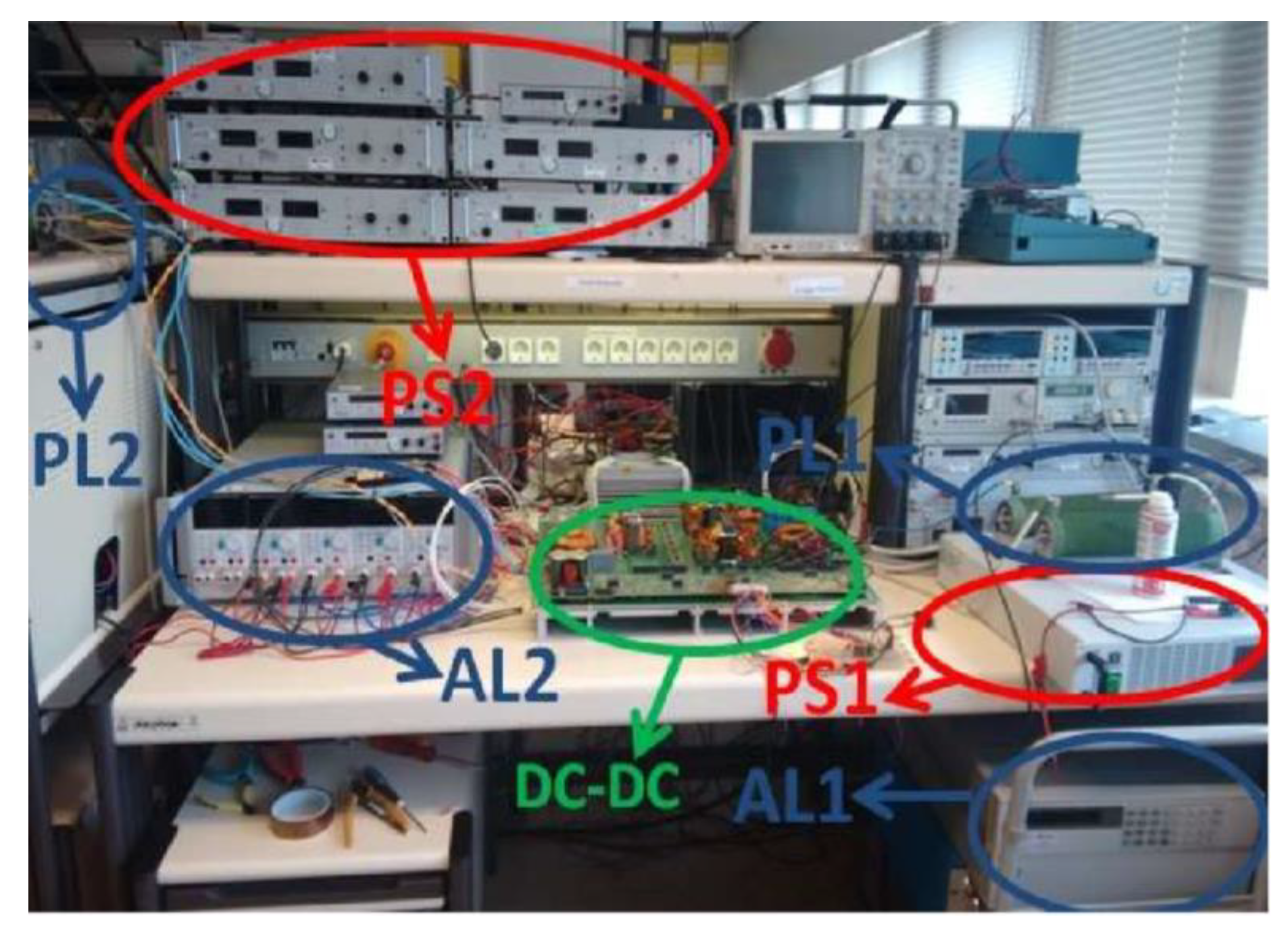
In Figure 13 a picture of the arranged test setup is shown, along with the highlighted parts.
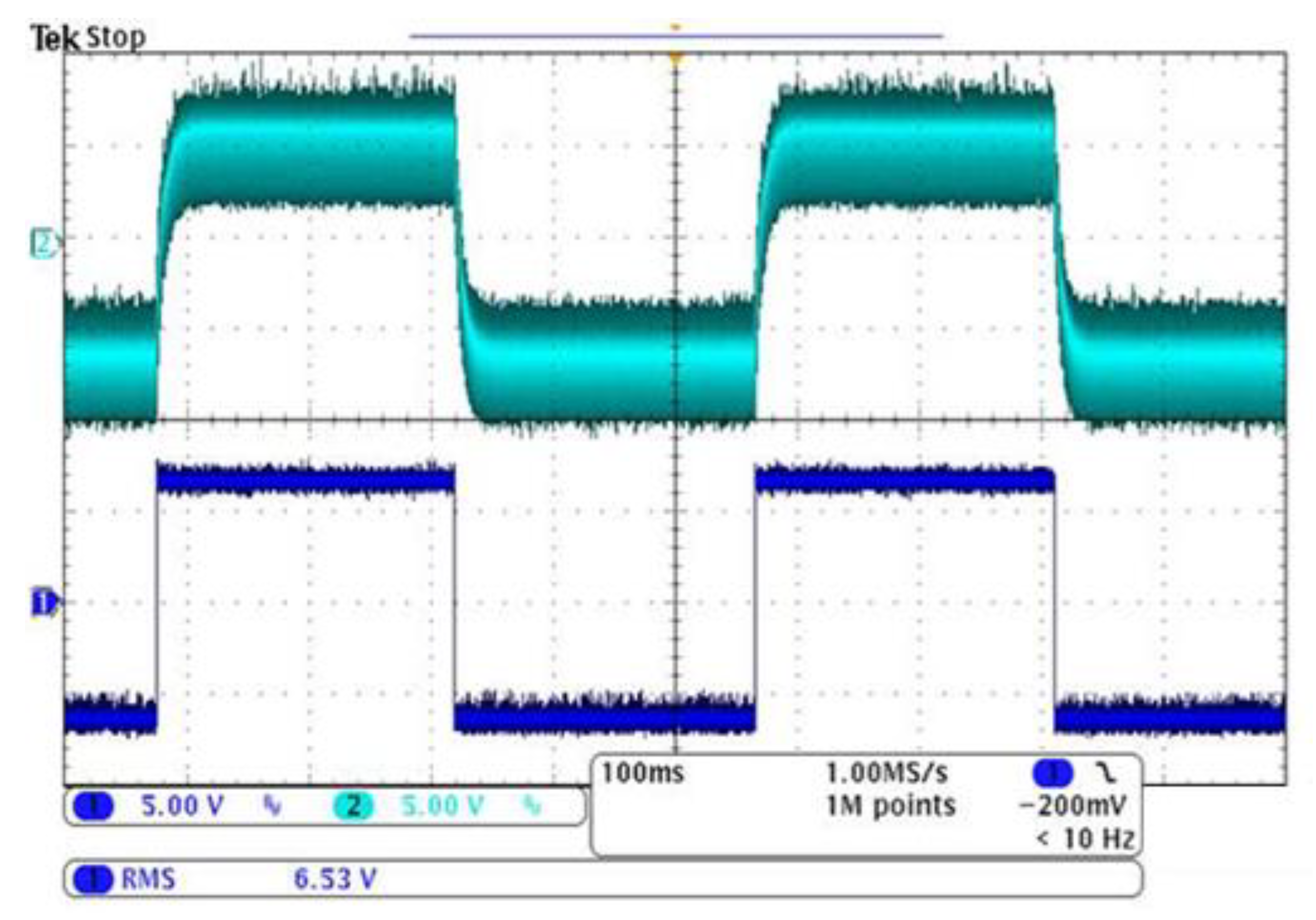
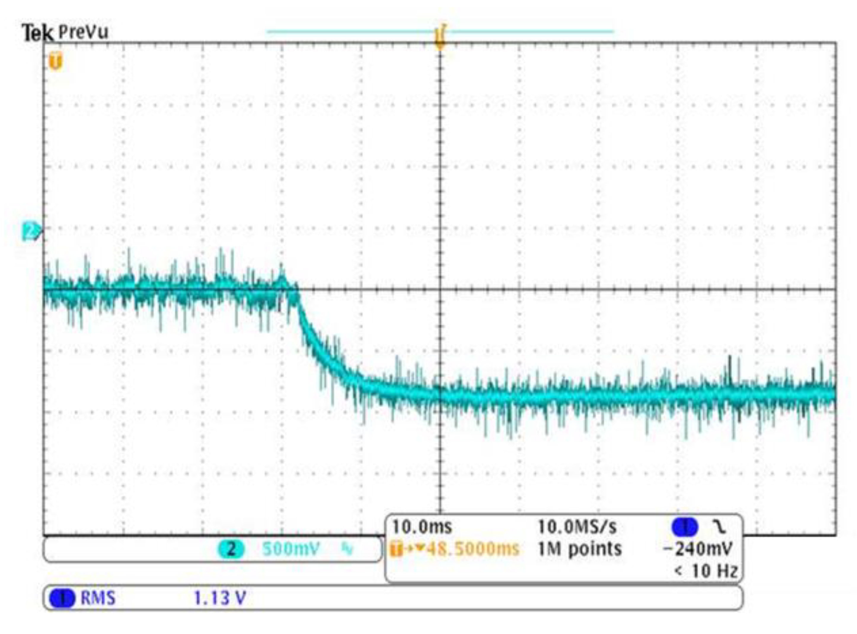
The improved PSM was implemented for the built prototype. The proper behavior of the converter is shown in Figure 14, showing the proper bus current response to a square wave command. The transduction factor in the command and monitoring signals is equal to 1 V/10% of full power, where “full power” corresponds to a 70 A bus current. Therefore, the image refers to a step between two levels corresponding to about 70% of the full negative power (during the SOSC recharge) and of the full positive power (during the SOSC discharge). There are no overshoot phenomena in the transients.
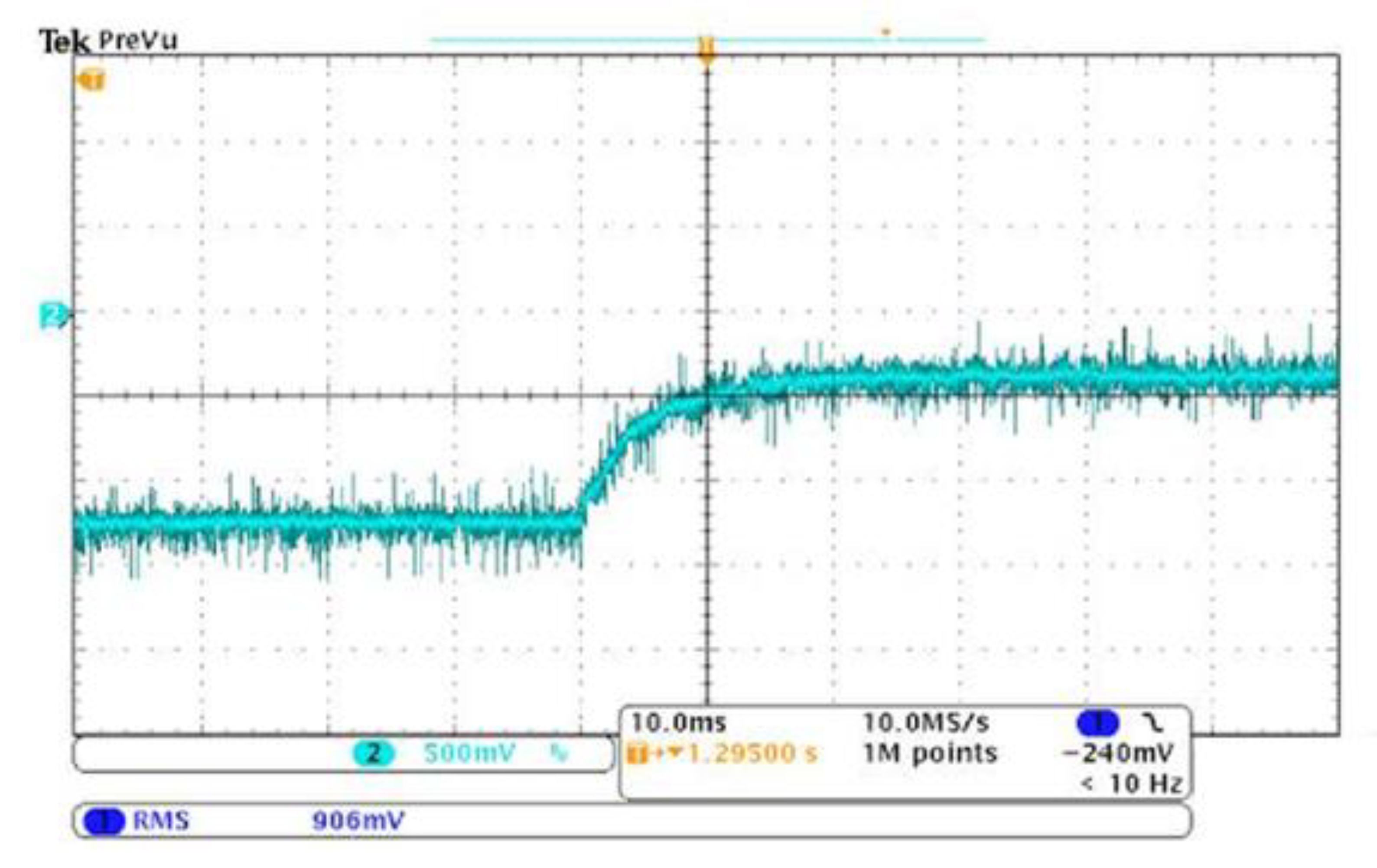
Figure 15 and Figure 16 show a zoom of the positive and negative transients respectively. Response time is compliant with the requirements, according to typical applications where 100 ms maximum response times are allowed. A further improvement of the response time is possible through a slight refinement of the control loop

5. Conclusions

In this paper, an insulated bidirectional DC-DC converter for the management of a storage system is proposed. Electrical Storage Systems find different possible application fields—automotive, zero-energy buildings, aerospace and so forth. The described topology is a Full-Bridge Converter (FBC), connected to a double voltage source—a voltage bus on one side and a Stack of Super-Capacitors (SOSC) on the other side. Analysis, design and modulation strategies of the proposed FBC are discussed. An improved modulation strategy has been proposed by authors, aiming at avoiding expensive clamping networks and at the power losses reduction. A 2 kW converter prototype, including also control and auxiliary power supply boards and compliant with automotive applications, has been realized and the related experimental results have been presented as well, proving the proper behavior of the converter.

Author Contributions

Conceptualization, F.P. and L.S.; Data curation, F.P. and G.S.; Investigation, F.V.; Methodology, L.S.; Project administration, R.M.; Software, G.S. and F.V.; Supervision, R.M.; Validation, F.P.; Visualization, G.S., F.V. and L.S.; Writing–original draft, F.P.; Writing–review & editing, R.M. All authors have read and agreed to the published version of the manuscript.

Funding

This work was financially supported by: MIUR-Ministero dell’Istruzione, dell’Università e della Ricerca (Italian Ministry of Education, University and Research), PON R&I 2014-2020-AIM (Attraction and International Mobility), project AIM1851228-1; AEROSPOWER Lab (Aerospace Power Laboratory) of Scuola di Ingegneria Aerospaziale, “Sapienza” University of Rome; ESA (European Space Agency), Contract No. 4000116941/16/NL/MH; Airbus Safran Launchers SAS; PON R&I 2015-2020 PROpulsione e Sistemi IBridi per velivoli ad ala fissa e rotante PROSIB, CUP no:B66C18000290005; PRIN 2017, Advanced power-trains and -systems for full electric aircrafts, prot. no.: 2017MS9F49; project REACTION (first and euRopEAn siC eighT Inches pilOt liNe), co-funded by the ECSEL Joint Undertaking under grant agreement No 783158; SDESLab (Sustainable Development and Energy Saving Laboratory) of University of Palermo; RPLab (Rapid Prototyping Laboratory-University of Palermo); LEAP (Laboratory of Electrical APplications) of University of Palermo.

Conflicts of Interest

The authors declare no conflict of interest.

References

  1. Livreri, P.; Caruso, M.; Castiglia, V.; Pellitteri, F.; Schettino, G. Dynamic reconfiguration of electrical connections for partially shaded PV modules: Technical and economical performances of an Arduino-based prototype. Int. J. Renew. Energy Res. 2018, 8, 336–344. [Google Scholar]
  2. Di Carlo, C.A.; Di Donato, L.; Mauro, G.S.; La Rosa, R.; Livreri, P.; Sorbello, G. A circularly polarized wideband high gain patch antenna for wireless power transfer. Microw. Opt. Technol. Lett. 2018, 60, 620–625. [Google Scholar] [CrossRef]
  3. La Rosa, R.; Zoppi, G.; Finocchiaro, A.; Papotto, G.; Di Donato, L.; Sorbello, G.; Bellomo, F.; Di Carlo, C.A.; Livreri, P. An over-the-distance wireless battery charger based on RF energy harvesting. In Proceedings of the 14th International Conference on Synthesis, Modeling, Analysis and Simulation Methods and Applications to Circuit Design (SMACD), Giardini Naxos, Italy, 12–15 June 2017; pp. 1–4. [Google Scholar]
  4. Yoo, H.; Sul, S.-K.; Park, Y.; Jeong, J. System integration and power-flow management for a series hybrid electric vehicle using supercapacitors and batteries. IEEE Trans. Ind. Appl. 2008, 44, 108–114. [Google Scholar] [CrossRef]
  5. Abdelhedi, R.; Chiheb Ammari, A.; Sari, A.; Lahyani, A.; Venet, P. Optimal power sharing between batteries and supercapacitors in Electric vehicles. In Proceedings of the 7th International Conference on Sciences of Electronics, Technologies of Information and Telecommunications (SETIT), Hammamet, Tunisia, 18–20 December 2016; pp. 97–103. [Google Scholar]
  6. Angerer, C.; Krapf, S.; Wassiliadis, N.; Lienkamp, M. Reduction of aging-effects by supporting a conventional battery pack with ultracapacitors. In Proceedings of the Twelfth International Conference on Ecological Vehicles and Renewable Energies (EVER), Monte Carlo, Monaco, 11–13 April 2017; pp. 1–12. [Google Scholar]
  7. Shah, N.; Czarkowski, D. Supercapacitors in Tandem with Batteries to Prolong the Range of UGV Systems. Electronics 2018, 7, 6. [Google Scholar] [CrossRef] [Green Version]
  8. Zhang, Q.; Li, G. Experimental Study on a Semi-Active Battery-Supercapacitor Hybrid Energy Storage System for Electric Vehicle Application. IEEE Trans. Power Electron. 2019, 35, 1014–1021. [Google Scholar] [CrossRef]
  9. Yaïci, W.; Kouchachvili, L.; Entchev, E.; Longo, M. Dynamic Simulation of Battery/Supercapacitor Hybrid Energy Storage System for the Electric Vehicles. In Proceedings of the International Conference on Renewable Energy Research and Applications (ICRERA), Brasov, Romania, 3–6 November 2019; pp. 460–465. [Google Scholar]
  10. Pellitteri, F.; Castiglia, V.; Livreri, P.; Miceli, R. Analysis and design of bi-directional DC-DC converters for ultracapacitors management in EVs. In Proceedings of the International Conference on Ecological Vehicles and Renewable Energies (EVER), Monte-Carlo, Monaco, 10–12 April 2018; pp. 1–6. [Google Scholar]
  11. Livreri, P.; Castiglia, V.; Pellitteri, F.; Miceli, R. Design of a Battery/Ultracapacitor Energy Storage System for Electric Vehicle Applications. In Proceedings of the 4th International Forum on Research and Technologies for Society and Industry (RTSI), Palermo, Italy, 10–13 September 2018; pp. 1–5. [Google Scholar]
  12. Castiglia, V.; Livreri, P.; Miceli, R.; Pellitteri, F.; Schettino, G.; Viola, F. Power Management of a Battery/Supercapacitor System for E-Mobility Applications. In Proceedings of the AEIT International Conference of Electrical and Electronic Technologies for Automotive (AEIT AUTOMOTIVE), Torino, Italy, 2–4 July 2019; pp. 1–5. [Google Scholar]
  13. Chakraborty, S.; Vu, H.N.; Hasan, M.M.; Tran, D.D.; Baghdadi, M.E.; Hegazy, O. DC-DC Converter Topologies for Electric Vehicles, Plug-in Hybrid Electric Vehicles and Fast Charging Stations: State of the Art and Future Trends. Energies 2019, 12, 1569. [Google Scholar] [CrossRef] [Green Version]
  14. Karbozov, A.; Ibanez, F.M. Optimal Design Methodology for High-Power Interleaved Bidirectional Buck-Boost Converters for Supercapacitors in Vehicular Applications. In Proceedings of the 8th International Conference on Renewable Energy Research and Applications (ICRERA), Brasov, Romania, 3–6 November 2019; pp. 152–157. [Google Scholar]
  15. Sadoun, R.; Rizoug, N.; Bartholumeus, P.; Barbedette, B.; LeMoigne, P. Sizing of hybrid supply (battery-supercapacitor) for electric vehicle taking into account the weight of the additional buck-boost chopper. In Proceedings of the First International Conference on Renewable Energies and Vehicular Technology, Hammamet, Tunisia, 26–28 March 2012; pp. 8–14. [Google Scholar]
  16. Camara, M.B.; Gualous, H.; Gustin, F.; Berthon, A. Design and new control of DC/DC converters to share energy between supercapacitors and batteries in hybrid vehicles. IEEE Trans. Veh. Technol. 2013, 57, 2721–2735. [Google Scholar] [CrossRef]
  17. Xue, L.K.; Wang, P.; Wang, Y.F.; Bei, T.Z.; Yan, H.Y. A four-phase high voltage conversion ratio bidirectional DC-DC converter for battery applications. Energies 2015, 8, 6399–6426. [Google Scholar] [CrossRef] [Green Version]
  18. Zhang, H.; Chen, Y.; Park, S.J.; Kim, D.H. A Family of Bidirectional DC–DC Converters for Battery Storage System with High Voltage Gain. Energies 2019, 12, 1289. [Google Scholar] [CrossRef] [Green Version]
  19. Lai, C.M. Development of a novel bidirectional DC/DC converter topology with high voltage conversion ratio for electric vehicles and DC-microgrids. Energies 2016, 9, 410. [Google Scholar] [CrossRef] [Green Version]
  20. Ikeda, S.; Kajiwara, K.; Tsuji, K.; Kurokawa, F. Efficiency improvement of isolated bidirectional boost full bridge dc-dc converter. In Proceedings of the 7th International Conference on Renewable Energy Research and Applications (ICRERA), Paris, France, 14–17 October 2018; pp. 673–676. [Google Scholar]
  21. Lee, I.O.; Lee, J.Y. A High-Power DC-DC Converter Topology for Battery Charging Applications. Energies 2017, 10, 871. [Google Scholar] [CrossRef]
  22. Shen, C.L.; Shen, Y.S.; Tsai, C.T. Isolated DC-DC Converter for Bidirectional Power Flow Controlling with Soft-Switching Feature and High Step-Up/Down Voltage Conversion. Energies 2017, 10, 296. [Google Scholar] [CrossRef] [Green Version]
  23. Pellitteri, F.; Boscaino, V.; Di Tommaso, A.O.; Miceli, R.; Capponi, G. Experimental test on a Contactless Power Transfer system. In Proceedings of the Ninth International Conference on Ecological Vehicles and Renewable Energies (EVER), Monte-Carlo, Monaco, 25–27 March 2014; pp. 1–6. [Google Scholar]
  24. Inoue, S.; Akagi, H. A bidirectional DC–DC converter for an energy storage system with galvanic isolation. IEEE Trans. Power Electron. 2007, 22, 2299–2306. [Google Scholar] [CrossRef]
  25. Pellitteri, F.; Caruso, M.; Castiglia, V.; Di Tommaso, A.O.; Miceli, R.; Schirone, L. An inductive charger for automotive applications. In Proceedings of the 42nd Annual Conference of the IEEE Industrial Electronics Society (IECON), Florence, Italy, 23–26 October 2016; pp. 4482–4486. [Google Scholar]
  26. Caruso, M.; Castiglia, V.; Di Tommaso, A.O.; Miceli, R.; Pellitteri, F.; Schirone, L. Efficient contactless power transfer system for EVs. In Proceedings of the 51st International Universities Power Engineering Conference (UPEC), Coimbra, Portugal, 6–9 September 2016; pp. 1–6. [Google Scholar]
  27. Pellitteri, F.; Boscaino, V.; Di Tommaso, A.O.; Miceli, R.; Capponi, G. Control subsystem design for wireless power transfer. In Proceedings of the International Conference on Renewable Energy Research and Application (ICRERA), Milwaukee, WI, USA, 19–22 October 2014; pp. 980–984. [Google Scholar]
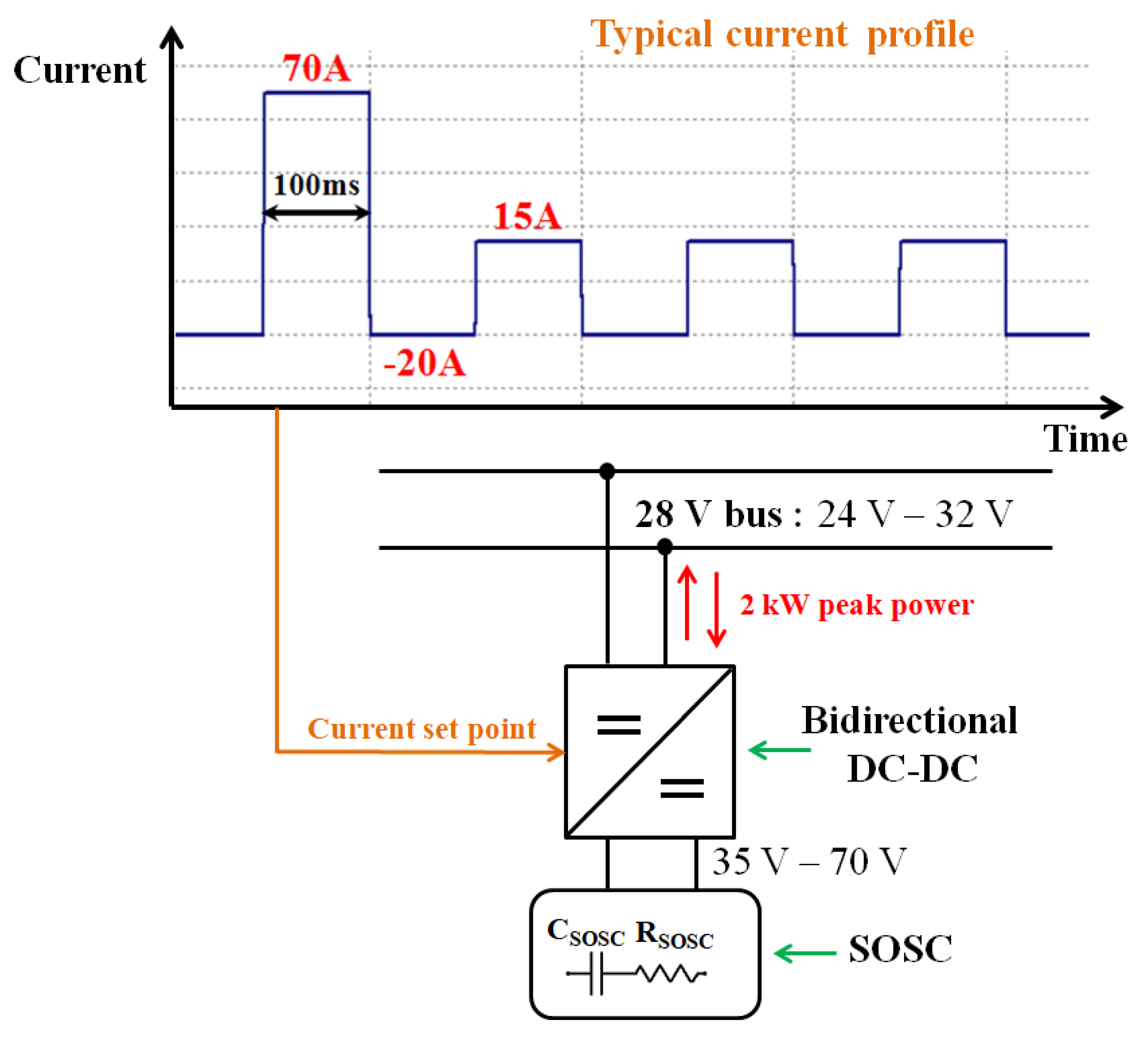
Figure 1. Power system architecture.
Electronics 09 00724 g001
Figure 2. Schematic of the Full Bridge Converter (FBC).
Electronics 09 00724 g002
Figure 3. Pulse Width Modulation (PWM) case: (a) gate signals; (b) modes of operation.
Electronics 09 00724 g003
Figure 4. Phase Shift Modulation (PSM) case: (a) gate signals; (b) modes of operation.
Electronics 09 00724 g004
Figure 5. Gate signals in conventional PSM.
Electronics 09 00724 g005
Figure 6. Secondary-side waveforms for the conventional PSM.
Electronics 09 00724 g006
Figure 7. Zoom on the secondary-side waveforms for the conventional PSM.
Electronics 09 00724 g007
Figure 8. Gate signals in modified PSM.
Electronics 09 00724 g008
Figure 9. Improved secondary-side waveforms for the modified PSM.
Electronics 09 00724 g009
Figure 10. Zoom on the secondary-side waveforms for the modified PSM.
Electronics 09 00724 g010
Figure 11. The prototype of the bidirectional FBC, as built and mounted.
Electronics 09 00724 g011
Figure 12. Schematic of the test setup.
Electronics 09 00724 g012
Figure 13. The arranged test setup.
Electronics 09 00724 g013
Figure 14. The proposed behavior of the bus current (in light blue), as experimentally tested, corresponding to a given power profile (in blue). For the monitoring signal (light blues) and the command signal (blue) 1 V is equivalent to the 10% of the full power.
Electronics 09 00724 g014
Figure 15. Zoom on a positive bus current transient, responding to an instantaneous positive command.
Electronics 09 00724 g015
Figure 16. Zoom on a negative bus current transient, responding to an instantaneous negative command.
Electronics 09 00724 g016
Table 1. Stack of Super-Capacitors (SOSC) parameters and voltage range.
CSOSCRSOSCVminVmax
4 F70 mΩ35 V70 V
Table 2. DC bus voltage minimum, nominal and maximum level.
VminVnomVmaz
24 V28 V32 V
Table 3. Efficiency at full power in case of SOSC recharge, as resulting from simulation.
Conventional PSM Improved PSM
V1V2ηV1V2η
70 V32 V0.7270 V32 V0.84
70 V24 V0.6270 V24 V0.80
35 V32 V0.7335 V32 V0.84
35 V24 V0.6735 V24 V0.85
Table 4. Characteristics of the realized transformer.
CoreMaterialnmMeasured LmMeasured L1
EE80/38/203C954660 μH140 nH
Table 5. Characteristics of the realized inductor.
CoreMaterialTurnsMeasured L2
00K7228E040Kool Mμ® 4013.524 μH
Table 6. Selected values of switching frequency and reactive components for the designed converter.
ParameterValue
fsw50 kHz
L224 μH
C1130 μF
C2200 μH