High-Speed Wide-Range True-Single-Phase-Clock CMOS Dual Modulus Prescaler


Abstract
1. Introduction
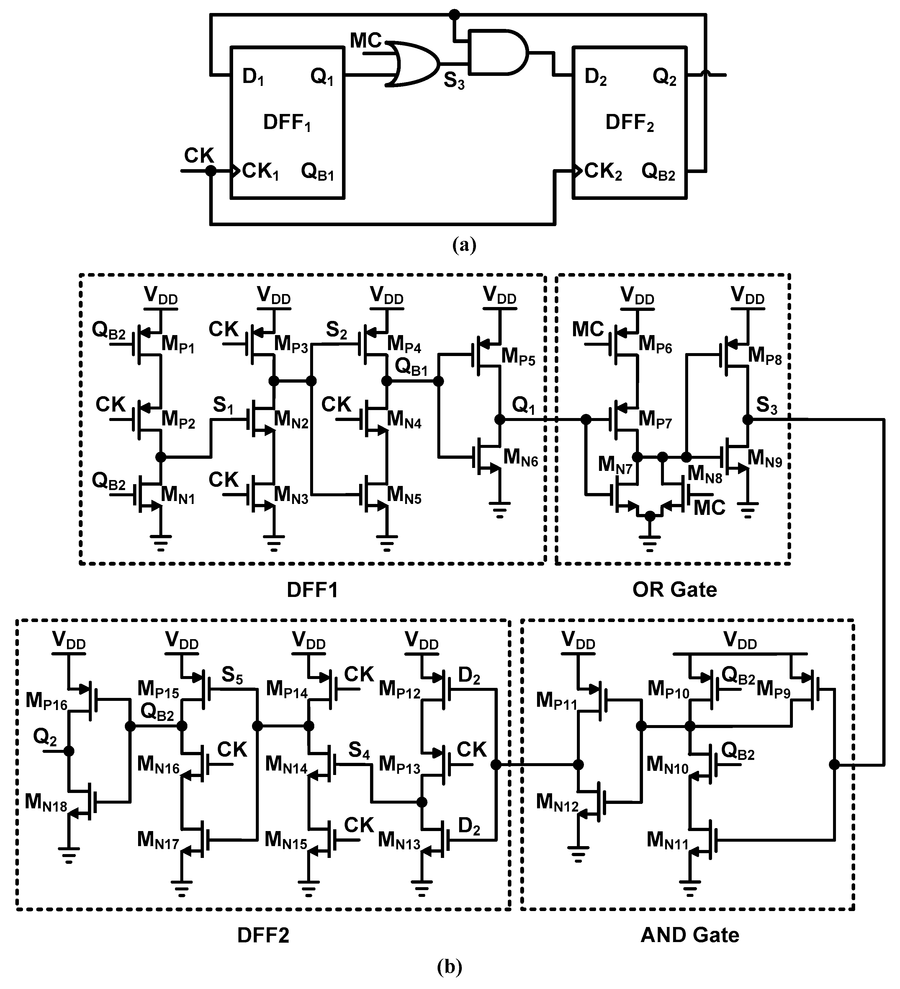
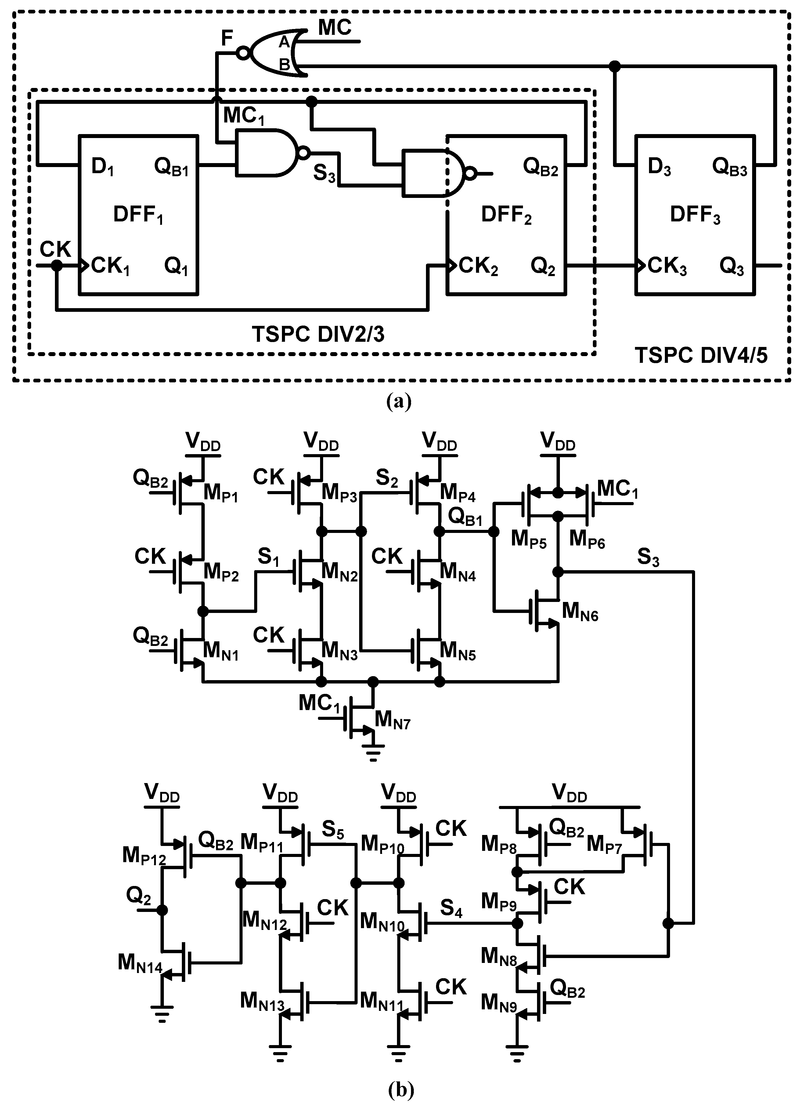
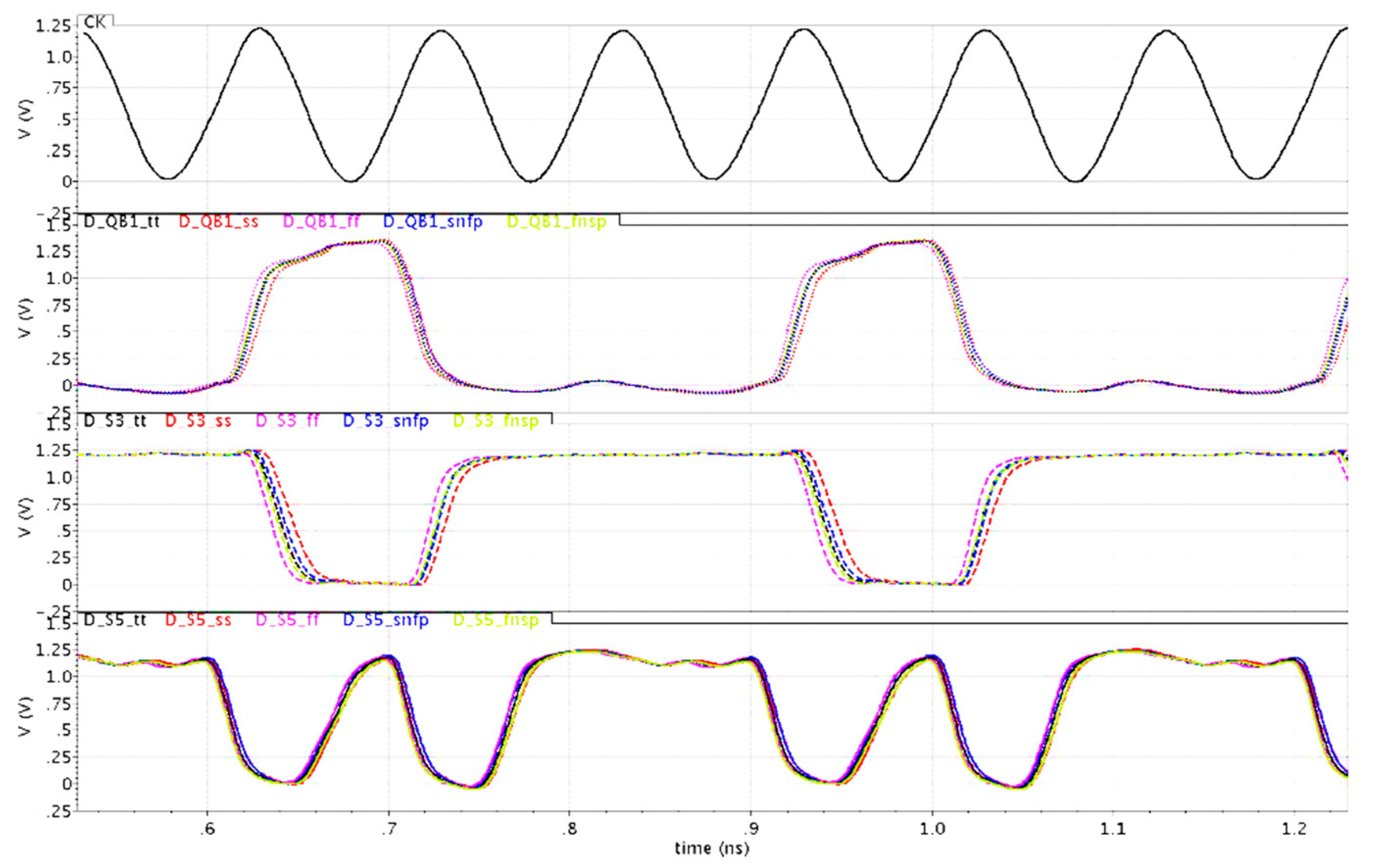
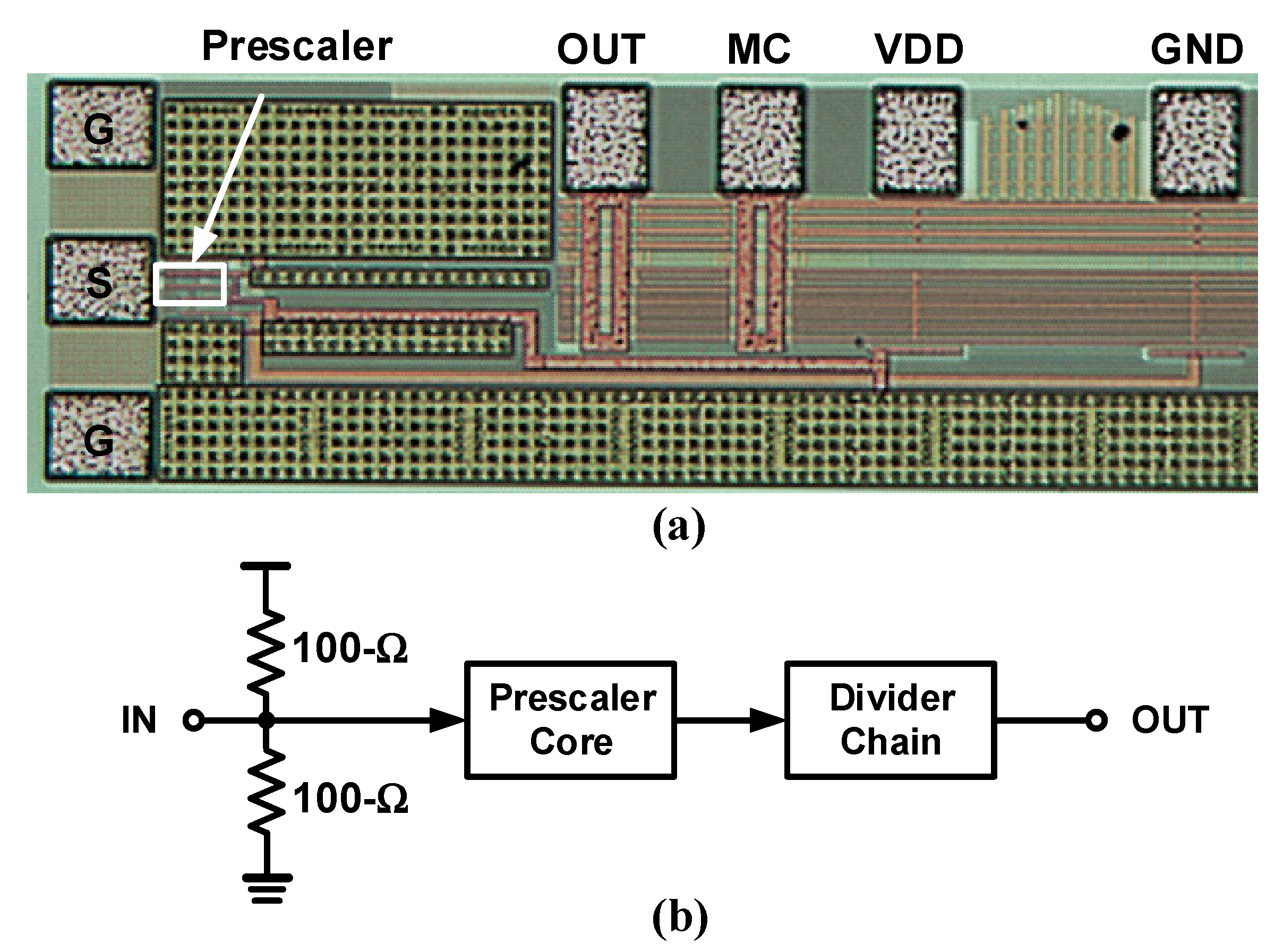
2. Circuit Design
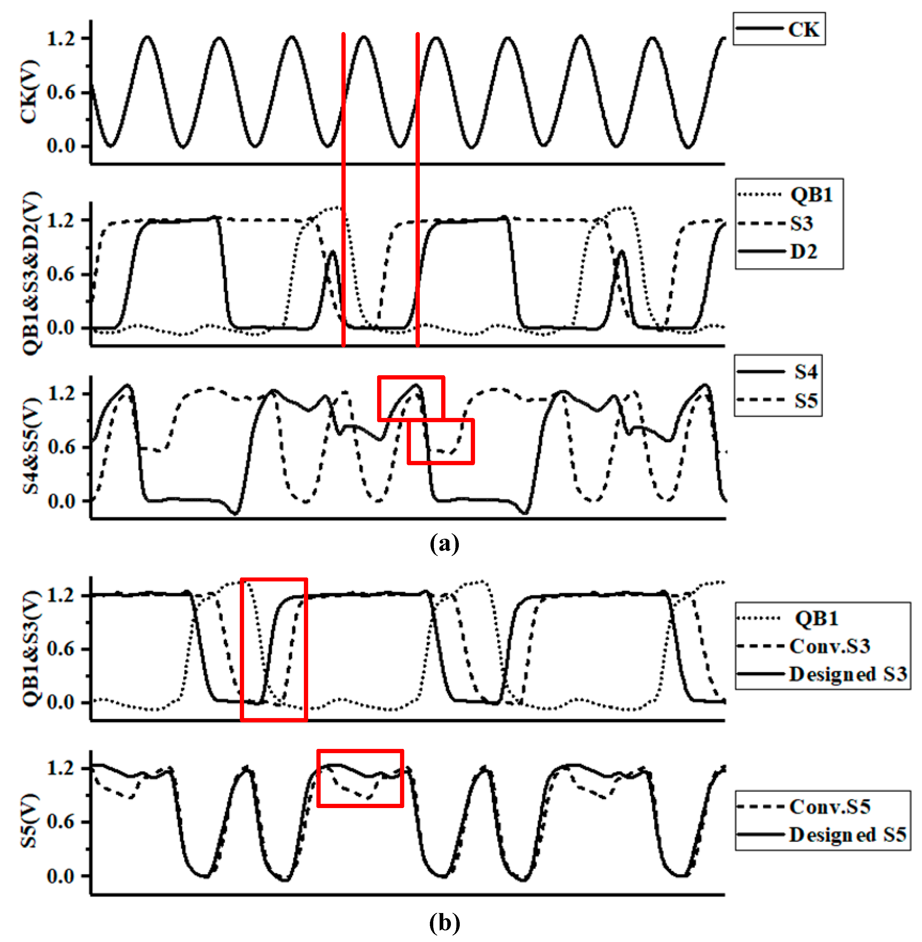
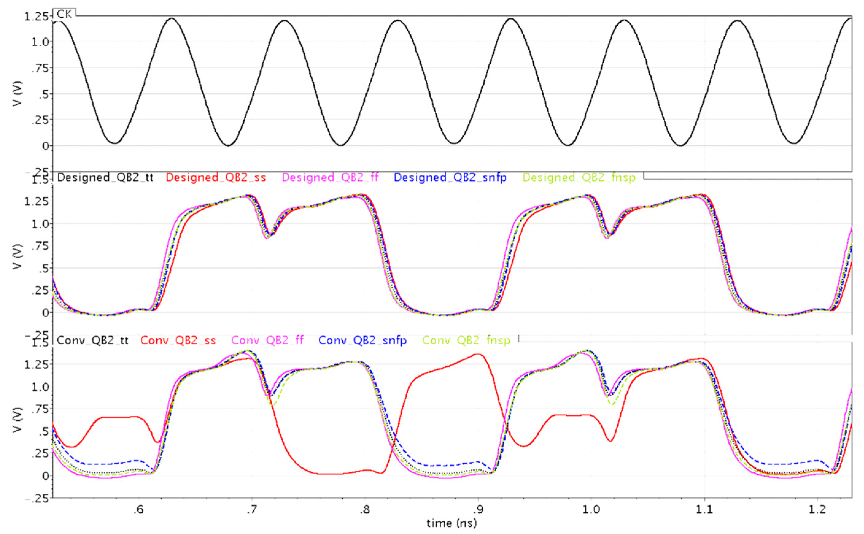
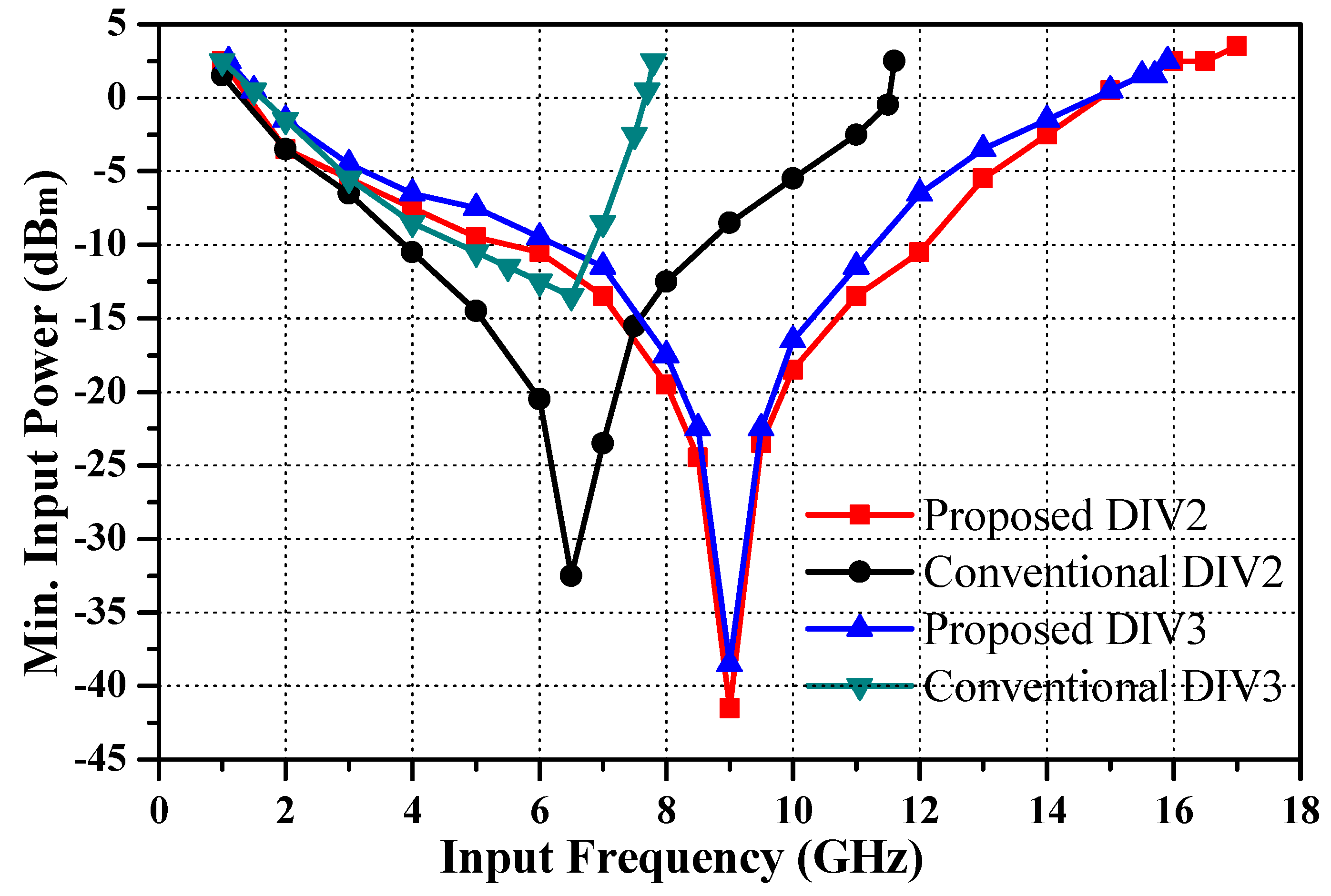
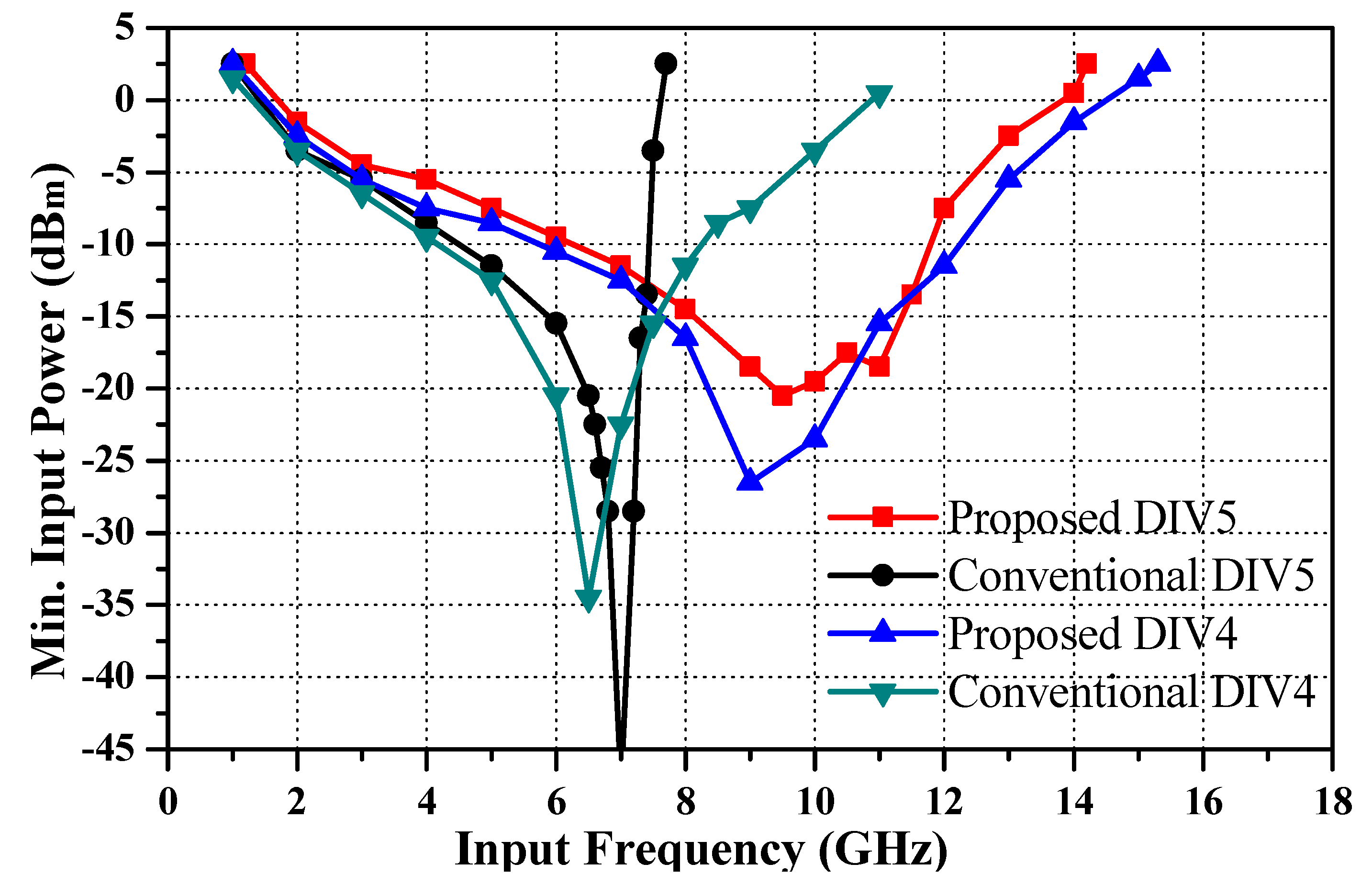
3. Measurement Results and Discussion
4. Conclusions
Author Contributions
Funding
Conflicts of Interest
References
- El-Halwagy, W.; Nag, A.; Hisayasu, P.; Aryanfar, F.; Mousavi, P.; Hossain, M. A 28-GHz Quadrature Fractional-N Frequency Synthesizer for 5G Transceivers with Less Than 100-fs Jitter Based on Cascaded PLL Architecture. IEEE Trans. Microw. Theory Tech. 2017, 65, 396–413. [Google Scholar] [CrossRef]
- Kim, N.; Rabaey, J.M. A 3.1–10.6-GHz 57-Bands CMOS Frequency Synthesizer for UWB-Based Cognitive Radios. IEEE Trans. Microw. Theory Tech. 2018, 66, 4134–4146. [Google Scholar] [CrossRef]
- Rategh, H.R.; Samavati, H.; Lee, T.H. A CMOS frequency synthesizer with an injection-locked frequency divider for a 5-GHz wireless LAN receiver. IEEE J. Solid-State Circuits 2000, 35, 780–787. [Google Scholar] [CrossRef]
- Manthena, V.K.; Do, M.A.; Boon, C.C.; Yeo, K.S. A Low-Power Single-Phase Clock Multiband Flexible Divider. IEEE Trans. Very Large Scale Integr. (VLSI) Syst. 2012, 20, 376–380. [Google Scholar] [CrossRef]
- Deng, Z.; Niknejad, A.M. The Speed–Power Trade-Off in the Design of CMOS True-Single-Phase-Clock Dividers. IEEE J. Solid-State Circuits 2010, 45, 2457–2465. [Google Scholar] [CrossRef]
- Chen, W.H.; Jung, B. High-Speed Low-Power True Single-Phase Clock Dual-Modulus Prescalers. IEEE Trans. Circuits Syst. II Exp. Briefs 2011, 58, 144–148. [Google Scholar] [CrossRef]
- Liu, F.; Wang, Z.; Li, Z.; Li, Q.; Yang, G.; Guo, T. Low-power 25.4–33.5 GHz programmable multi-modulus frequency divider. Electron. Lett. 2014, 5050, 1067–1068. [Google Scholar] [CrossRef]
- Gu, Q.J.; Gao, Z. A CMOS high speed multi-modulus divider with retiming for jitter suppression. IEEE Microw. Wirel. Compon. Lett. 2013, 23, 554–556. [Google Scholar] [CrossRef]
- Shi, J.; Mo, T.; Ma, C.; Ye, T. A current-shaping technique for static MOS current-mode logic prescalers. IEICE Electron. Express 2013, 10, 20120887. [Google Scholar] [CrossRef]
- Tsai, J.-H.; Chung, Y.-W.; Shih, H.-D.; Chou, J.-P. A 7-12 GHz Multi-Modulus Frequency Divider. In Proceedings of the Asia Pacific Microwave Conference Proceedings, Kaohsiung, Taiwan, 4–7 December 2012; pp. 1232–1234. [Google Scholar]
- Vigilante, M.; Reynaert, P. A 25-102GHz 2.81-5.64mW Tunable Divide-by-4 in 28nm CMOS. In Proceedings of the IEEE Asian Solid-State Circuits Conference (ASSCC), Xiamen, China, 9–11 November 2015; pp. 1–4. [Google Scholar]
- Razavi, B. TSPC logic [a circuit for all seasons]. IEEE Solid-State Circuits Mag. 2016, 8, 10–13. [Google Scholar] [CrossRef]
- Hwang, Y.; Lin, J. Low Voltage and Low Power Divide-By-2/3 Counter Design Using Pass Transistor Logic Circuit Technique. IEEE Trans. Very Large Scale Integr. (VLSI) Syst. 2012, 20, 1738–1742. [Google Scholar] [CrossRef]
- Jia, S.; Wang, Z.; Li, Z.; Wang, Y. A Novel Low-Power and High-Speed Dual-Modulus Prescaler Based on Extended True Single-Phase Clock Logic. In Proceedings of the IEEE International Symposium on Circuits and Systems (ISCAS), Montreal, QC, Canada, 22–25 May 2016; pp. 2751–2754. [Google Scholar]
- Shen, T.; Liu, J.; Song, C.; Xu, Z. A High-Speed Low-Power Divide-by-3/4 Prescaler using E-TSPC Logic DFFs. Electronics 2019, 8, 589. [Google Scholar] [CrossRef]
- Wang, W.; Jia, S.; Wang, Z.; Pan, T.; Wang, Y. Low Voltage Dual-Modulus Frequency Divider Based on Extended True Single-Phase Clock Logic. In Proceedings of the IEEE International Conference on Electron Devices and Solid State Circuits (EDSSC), Shenzhen, China, 6–8 June 2018; pp. 1–2. [Google Scholar]
- Krishna, M.V.; Do, M.A.; Yeo, K.S.; Boon, C.C.; Lim, W.M. Design and Analysis of Ultra Low Power True Single Phase Clock CMOS 2/3 Prescaler. IEEE Trans. Circuits Syst. I Reg. Pap. 2010, 57, 72–82. [Google Scholar] [CrossRef]
- Tooprakai, S.; Wisetphanichkij, S.; Tudsorn, A. A 1.1-V Low Power True Single-Phase Clock 2/3 Prescaler. In Proceedings of the International Electrical Engineering Congress (iEECON), Pattaya, Thailand, 8–10 March 2017; pp. 1–4. [Google Scholar]
- Jiang, W.; Yu, F. 4.2 GHz 0.81 mW Triple-Modulus Prescaler Based on True Single-Phase Clock. Electron. Lett. 2016, 52, 1007–1008. [Google Scholar] [CrossRef]
- Zhu, W.; Yang, H.; Gao, T.; Liu, F.; Yin, T.; Zhang, D.; Zhang, H. A 5.8-GHz Wideband TSPC Divide-by-16/17 Dual Modulus Prescaler. IEEE Trans. Very Large Scale Integr. (VLSI) Syst. 2015, 23, 194–197. [Google Scholar]
- Chen, W.H.; Roa, E.; Loke, W.F.; Jung, B. A 14.1-GHz Dual-modulus Prescaler in 130nm CMOS Technology Using Sequential Implication Logic Cells. In Proceedings of the IEEE Radio Frequency Integrated Circuits Symposium (RFIC), Montreal, QC, Canada, 17–19 June 2012; pp. 341–344. [Google Scholar]
- Krishna, M.V.; Jain, A.; Quadir, N.A.; Townsend, P.D.; Ossieur, P. A 1V 2mW 17GHz Multi-Modulus Frequency Divider Based on TSPC Logic Using 65nm CMOS. In Proceedings of the ESSCIRC 2014-40th European Solid State Circuits Conference (ESSCIRC), Venice Lido, Italy, 22–26 September 2014; pp. 431–434. [Google Scholar]
- Jiang, W.; Yu, F.; Huang, Q. A Low-Power High-speed True Single-Phase Clock-Based Divide-By-2/3 Prescaler. IEICE Electron. Express 2017, 14, 20160446. [Google Scholar] [CrossRef][Green Version]
- Jia, S.; Yan, S.; Wang, Y.; Zhang, G. Low-power, High-Speed Dual Modulus Prescalers Based on Branch-Merged True Single-Phase Clocked Scheme. Electron. Lett. 2015, 51, 464–465. [Google Scholar] [CrossRef]
- Silva-Pereira, M.; Caldinhas Vaz, J. Power optimization of both a high-speed counter and a retiming element for 2.4 GHz digital PLLs. Electron. Lett. 2018, 54, 284–285. [Google Scholar] [CrossRef]
- Stas, F.; Bol, D. A 0.4-V 0.66-fJ/cycle Retentive True-Single-Phase-Clock 18T Flip-Flop In 28-Nm Fully-Depleted SOI CMOS. IEEE Trans. Circuits Syst. I Reg. Pap. 2018, 65, 935–945. [Google Scholar] [CrossRef]
- Shaikh, J.; Rahaman, H. High Speed and Low Power Preset-Able Modified TSPC D Flip-Flop Design and Performance Comparison with TSPC D Flip-Flop. In Proceedings of the International Symposium on Devices, Circuits and Systems (ISDCS), Howrah, India, 29–31 March 2018; pp. 1–4. [Google Scholar]
- Li, Y.; Shin, G.; Li, Y. A Fully Static True-Single-Phase-Clocked Dual-Edge-Triggered Flip-Flop for Near-Threshold Voltage Operation in IoT Applications. IEEE Access 2020, 8, 40232–140245. [Google Scholar]
- Lin, J.; Sheu, M.; Hwang, Y.; Wong, C.; Tsai, M. Low-Power 19-Transistor True Single-Phase Clocking Flip-Flop Design Based on Logic Structure Reduction Schemes. IEEE Trans. Very Large Scale Integr. (VLSI) Syst. 2017, 25, 3033–3044. [Google Scholar] [CrossRef]
- Szilagyi, L.; Li, S.; Xu, X.; Testa, P.V.; Gunia, M.; Seidel, A.; Carta, C.; Finger, W.; Ellinger, F. A Divide-by-4 and -8 Circuit for 77 GHz Radar in 22 nm FD-SOI CMOS. In Proceedings of the 4th Australian Microwave Symposium (AMS), Sydney, Australia, 13–14 February 2020. [Google Scholar]
- Cai, Y.; Savanth, A.; Prabhat, P.; Myers, J.; Weddell, A.S.; Kazmierski, T.J. Ultra-Low Power 18-Transistor Fully Static Contention-Free Single-Phase Clocked Flip-Flop in 65-nm CMOS. IEEE J. Solid-State Circuits 2019, 54, 550–559. [Google Scholar] [CrossRef]
- Yue, C.; Howard, C.L.; Zhiliang, H. Analysis and Design of a 14.1-mW 50/100-GHz Transformer-Based PLL With Embedded Phase Shifter in 65-nm CMOS. IEEE Trans. Microw. Theory Tech. 2015, 63, 1193–1201. [Google Scholar]
- Lo, Y.; Ho, W. A Low-Voltage PLL Design Using a New Calibration Technique for Low-Power Implantable Biomedical Systems. Circuits Syst. Signal Process. 2017, 36, 4809–4828. [Google Scholar] [CrossRef]


| Design | Process | Division Ratio | Freq. Range (GHz) | Power (mW) * | Chip Area (μm2) |
|---|---|---|---|---|---|
| [19] | 180 nm | 6/7/8 | 0.2–4.2 | 0.81 ** | 35 × 40 |
| [20] | 180 nm | 16/17 | 0.002–5.8 | 2.2 | 40 × 80 |
| [21] | 130 nm | 2/3 | 14.1 | 0.8/1.1 | - |
| [22] | 65 nm | 2/3 4/5 | 17 *** | 0.318 0.938 | - |
| [23] | 180 nm | 2/3 | 0.7–5.7 | 0.95 | 30 × 40 |
| [30] | 22 nm | /4, /8 | 10–64 | 2.2 ** | 154 |
| This work | 90 nm | 2/3 | 1–17/ 1.1–15.9 | 0.67/0.92 | 20 × 35 |
| This work | 90 nm | 4/5 | 1–15.3/ 1.2–14.2 | 0.87/1.06 | 20 × 50 |
© 2020 by the authors. Licensee MDPI, Basel, Switzerland. This article is an open access article distributed under the terms and conditions of the Creative Commons Attribution (CC BY) license (http://creativecommons.org/licenses/by/4.0/).
Share and Cite
Li, X.; Gao, J.; Chen, Z.; Wang, X. High-Speed Wide-Range True-Single-Phase-Clock CMOS Dual Modulus Prescaler. Electronics 2020, 9, 725. https://doi.org/10.3390/electronics9050725
Li X, Gao J, Chen Z, Wang X. High-Speed Wide-Range True-Single-Phase-Clock CMOS Dual Modulus Prescaler. Electronics. 2020; 9(5):725. https://doi.org/10.3390/electronics9050725
Chicago/Turabian StyleLi, Xiaoran, Jian Gao, Zhiming Chen, and Xinghua Wang. 2020. "High-Speed Wide-Range True-Single-Phase-Clock CMOS Dual Modulus Prescaler" Electronics 9, no. 5: 725. https://doi.org/10.3390/electronics9050725
APA StyleLi, X., Gao, J., Chen, Z., & Wang, X. (2020). High-Speed Wide-Range True-Single-Phase-Clock CMOS Dual Modulus Prescaler. Electronics, 9(5), 725. https://doi.org/10.3390/electronics9050725