Article

Minimization of Network Induced Jitter Impact on FPGA-Based Control Systems for Power Electronics through Forward Error Correction

1
Department of Engineering and Architecture, University of Parma, Parco Area delle Scienze, 181/A, 43124 Parma, Italy
2
Faculty of Science and Engineering, University of Nottingham Ningbo, 199 Taikang East Road, Ningbo 315100, China
3
Department of Engineering “Enzo Ferrari”, University of Modena and Reggio Emilia, lVia P. Vivarelli, 10, 41125 Modena, Italy
*
Author to whom correspondence should be addressed.
Electronics 2020, 9(2), 281; https://doi.org/10.3390/electronics9020281
Submission received: 19 December 2019 / Revised: 27 January 2020 / Accepted: 4 February 2020 / Published: 6 February 2020
(This article belongs to the Section Power Electronics)

Abstract

:
In modular distributed architectures, the adoption of a communication method that is at the same time robust and has a low and predictable latency is of utmost importance in order to support the required system dynamics. The aim of this paper is to evaluate the consequences of the random jitter on machine drives distributed control, caused by the messages’ re-transmission in case of an error in the received data. To achieve this goal, two different Forward Error Correction (FEC) techniques are introduced in the chosen protocol, so that the recipient of the message can correct random errors without the need of any additional round trip delays needed to request and obtain a re-transmission. Experimentally validated simulations are used to evaluate the impact of random network derived jitter on a real world closed loop control system for distributed power electronic converters.

1. Introduction

The modern scenario for power electronics is of one of ever increasing complexity with radical paradigm shifts in many sectors. On the power distribution side, the advent of renewable energies has brought forward a set of challenges [1] that can be solved by moving from a traditional transformer-based, unidirectional power distribution network to smart grids. In this context, static power converters can more easily allow for bidirectional power flow while helping to maintain overall grid stability, by employing a wide array of control techniques [2]. The pervasive electrification of the transportation sector is also driving up power electronics complexity, for both cars [3] with the introduction of hybrid and electric vehicles, and aircraft [4]. In fact, the More Electric Aircraft (MEA) [5] framework aims to replace the mechanical, hydraulic, and pneumatic systems with electromechanical ones. This will lead to an increase in overall efficiency through the use of a more effective, bleedless turbofan main engine, and to weight reduction due to the elimination of ducting, valving, and other power transmission components. In these types of systems, fault tolerance is one of the most important design aspects. This goal can be achieved again through modularization, adopting segmented motors, and drives [6].
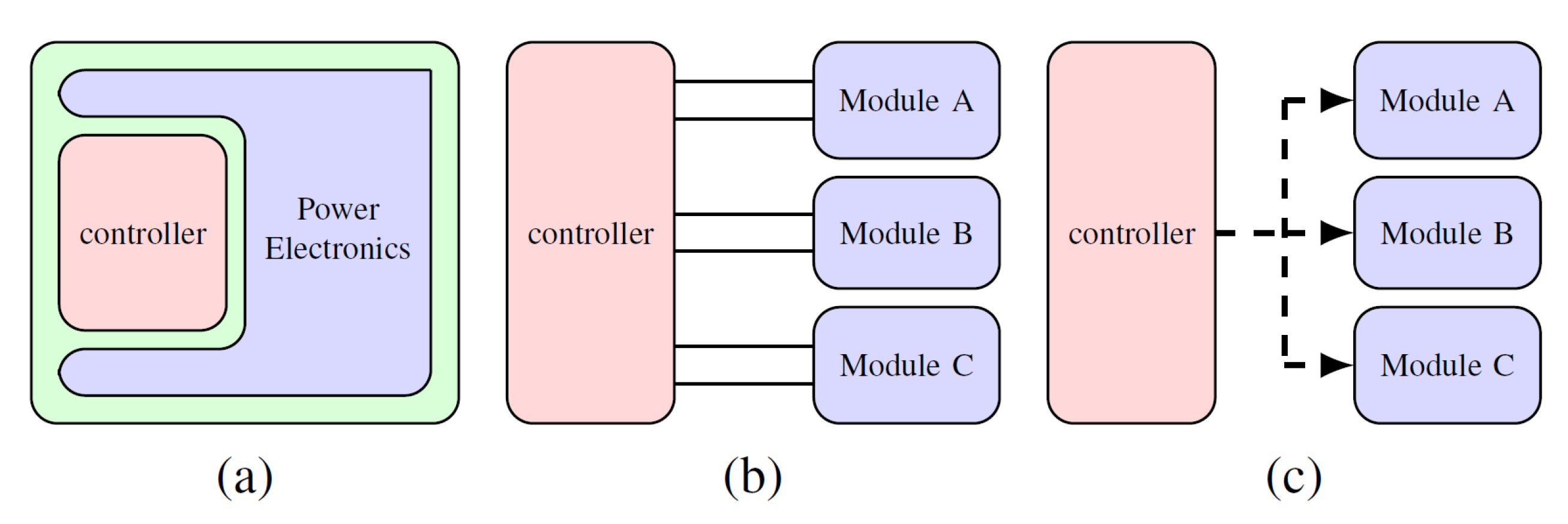
Traditional architecture for power converters and machine drives relies on a single inverter driving a three-phase electrical machine, as shown in Figure 1a. In segmented drives, conversely, the electrical machine is designed with multi three-phase windings, each of them driven by a separated power electronics module (inverter). The different power modules jointly contribute to drive the electrical machines in a distributed way, making the system intrinsically more reliable and resilient. A single centralized controller (master controller, Figure 1b) can still be employed for both control loop execution and direct gate signal generation for the power modules. However, the high number of power devices used in modular power conversion setups, makes this impractical. In addition, the reliability of direct gate signal distribution, in the increasingly distributed system, is also lower as the electromagnetic noise, inherently generated by the switching action, can cause an unwanted device commutation with catastrophic consequences. A different approach that could solve this issues is a different architecture, moving from a classical to a networked control system, where each sub-module generates the gate signals locally, as shown in Figure 1c. This transition is made more complex by the lack of a communication protocol specifically designed for these tasks, thus forcing designers of power converters to use industrial automation targeted ones. Few efforts have been made to introduce more modern communication techniques to power electronics [7]. In [8], a custom UDP (User Datagram Protocol) implementation on top of a 100BASE-TX ethernet link is proposed, however the reliance on standard protocol for the first and second OSI layers, leads to a very large transmission delay that makes the system unsuitable for state-of-the-art high frequency power electronic converters. Another approach is presented in [9], where the authors use a commercial off-the-shelf transceiver integrated circuit (now discontinued), originally meant for server and backplane applications, based on an optical fiber link in order to achieve better performance. The downside of what is presented here is a complete reliance on the availability of this circuit, which is problematic, not only because it limits the flexibility of the resulting system, but also because it poses long term availability issues.
In this scenario, the adoption of a communication method that is at the same time robust and has a low and predictable latency is of the utmost importance in order to support the required system dynamics [10]. Along with the latency, the jitter introduced in the system by the network layer is particularly problematic. In fact, it is inherent to the protocol that uses error detection and subsequent re-transmission to ensure the correctness of the received messages, that will thus be delayed by an amount of time that is dependent on both protocol and channel conditions. Forward Error Correction (FEC) techniques can instead be used in order to ensure the absence of errors on the link, even when the channel conditions are not ideal, without the need to request and wait for a full message re-transmission by the master controller. Several well-established techniques [11,12], already used in other networking settings, can be re-purposed as long as performance in terms of payload integrity, low latency, and low jitter can match the peculiar requirements of this application.
The application of FEC techniques to power electronics has been recently studied, especially in the context of smart grids [13,14], where the low operating frequencies and large impedance of the network do not require large control system bandwidth, as in the field of machine drives. The core problem that has slowed the widespread adoption of FEC techniques is the large latency associated with Microcontroller or DSP (Digital Signal Processor) implementation. Even when using state-of-the-art algorithms on modern hardware [15], the calculations still require several hundreds of microseconds, which is too much when targeting system sampling frequencies in the tens of kHz, as is typical for these applications. Only recently, the availability of low cost, high density Field Programmable Gate Arrays (FPGA) has also allowed the use of these techniques in the filed of machine drives. In [16], a communication protocol for optical fibers-based distributed power electronic systems is developed. However, in [13,14,16] a comprehensive evaluation of the impact of the introduction of digital communication to the control of distributed drive applications is still not fully examined. In particular, how FEC techniques can reduce the vulnerability of a control system to network-related jitter is still an open issue. The aim of this paper, is hence to investigate the impact of FEC techniques in power electronics systems and their control, considering the particular requirements of very low jitter and small payload sizes encountered in this specific field.
The paper is organized as follows. In Section 2, used communication protocol and FEC techniques are introduced. In Section 3, implementations are detailed, whereas in Section 4, the effects of latency in a distributed drive control loop are discussed. In Section 5, experimental results are discussed and finally, in Section 6 conclusions are drawn.

2. Communication Protocol

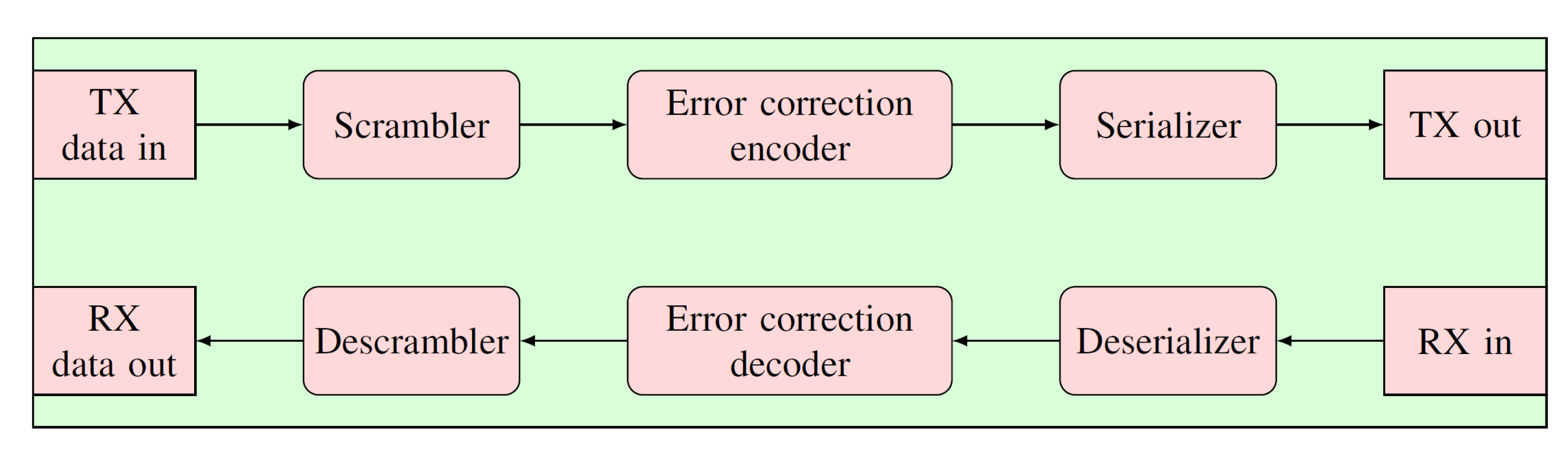
The aim of the designed communication protocol is to enable the exchange of control information from a master controller to one or more nodes, with as little latency or jitter as possible. The overall structure of the communication protocol implementation can be found in Figure 2.

2.1. Synchronization

The primary problem to solve when designing distributed networks of any kind is the need for synchronization, in order to enable the various nodes composing the system to act in a coherent way. Several techniques [17] can be used for this purpose, for example, clock distribution networks, preamble synchronization, clock embedding, and scrambling-based clock recovery with periodic transmissions.
The first solution is very attractive, making the implementation of the communication protocol much easier as the synchronization is guaranteed by the physical distribution of clock signals throughout the system. Despite its simplicity, this solution is rarely used in practice as it shifts the complexity and reliability issued on a physical level, requiring extra conductors and more elaborate and expensive connectors. With preamble synchronization these problems are addressed by shifting the clock signal in band. In this case, an alternating bit pattern is transmitted at the start of each message, enabling the receiver to lock the internal oscillator to it. Following this solution, the extra clock distribution hardware is removed and thus reduces system complexity. The downside of this is a less efficient use of the channel bandwidth as extra information has to be transmitted.
Similarly, the second technique includes a synchronization signal in band, but instead of transmitting it before the message, it is embedded in the signal itself by the use of a suitable line encoding (e.g., Manchester encoding, 8 b/10 b, etc.). The first field of application of this method is for messages with small payloads where it can have a lower impact with respect to the addition of a preamble, whose size is determined only by the characteristics of the receiver clocking system.
The last technique to be taken into consideration is based on the periodic transmission of scrambled data. This, while requiring additional complexity, can guarantee clock synchronization at no additional costs in terms of packet size. This technique has been adopted in this paper as the receiver employs a phase locked loop to synchronize the system clock with the incoming signal edges. In order to guarantee a sufficient amount of signal transitions, a multiplicative, self-synchronizing [18] scrambler is used, along with a minimum packet transmission frequency.

2.2. Error Handling

The next problem that the protocol needs to solve is the protection against errors in order to ensure communication reliability. The simplest error handling technique that can be used is error detection and re-transmission. Thanks to appropriate algorithms, the receiver can evaluate the integrity of the received data [
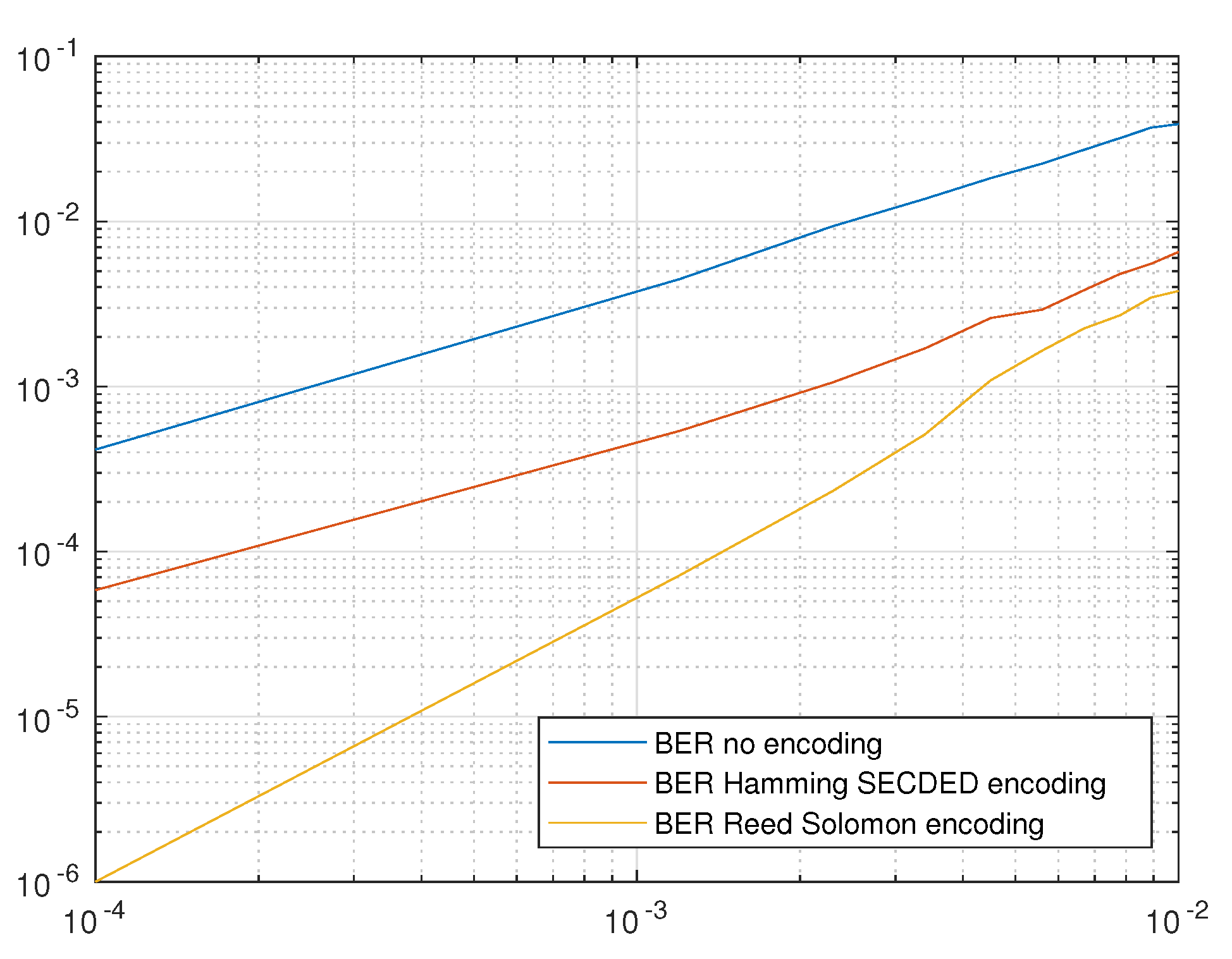
19]. The downside of this approach are the large latency spikes on the communication channel when a re-transmission is required. FEC, by contrast, focuses on trying to add just enough redundancy to enable the correction of errors most likely to occur. The main advantage is the ability to significantly reduce latency variance by avoiding re-transmissions. This comes at the cost of higher complexity and a limited number of correctable errors, depending on the chosen type of coding. In order to guarantee an error free communication, a balance must be determined between FEC technique strength and the physical channel minimum Signal to Noise Ratio (SNR). The SNR strongly depends on the chosen physical channel and/or transceiver, that differ in each application. Depending on the application, it will be necessary to estimate the desired minimum SNR and choose the better FEC technique, considering the best compromise between its strength and its complexity. For this reason, in this paper three cases with increasing error correction capacity will be compared: The uncoded modulation, a Hamming, and a Reed–Solomon (RS) coding.

2.3. Compared Algorithms Details

In this work, two different FEC methods have been compared, Hamming and RS coding. An unprotected communication stream is also evaluated serving as a baseline. In the studied application the minimal practical payload length is of 40 bits, chosen as a compromise between bandwidth efficiency and transmission delay.
The first considered algorithm is a shortened SECDED (Single-Error Correcting and Double-Error Detecting) Hamming code that can detect two bit errors, by transmitting along with the payload (up to k H = 40 bits) a number of different “parity” bits (this number, denoted with m H , is usually equal to 6). The first step in order to construct this code is the choice of a perfect Hamming code [20], that can encode enough information to fit the entire message. The redundant information bits are then removed, in an operation called shortening. The last step is to apply a standard checksum, increasing the Hamming distance of the resulting code, enabling the double error detection. A second class of studied algorithms are RS codes, a class of q-ary block codes operating over the q ( q > 2 ) elements of the Galois Field GF(q) [21]. A RS code is defined by the following parameters: m is the number of bits per symbol, k is the number of data symbols, 2 t is the number of parity symbols, and n is the total length of the coded word ( n = k + 2 t ). A RS code with these parameters is able to correct up to t errors in the received word. Since RS code theory is based on Galois Field (GF) mathematics, to perform encoding and decoding two polynomials have to be defined: The primitive (or field generator) polynomial, from which all elements in a GF can be generated, and the code generator polynomial, the roots of which are consecutive elements in the GF. Their choice is of particular importance as it can greatly simplify the decoder architecture. The values for all the parameters used in this study are shown in Table 1 and Table 2.

3. Implementation

Several different factors have steered the choice of the device for the implementation of the designed protocol and the studied error correction. The use of a traditional Microcontroller or DSP-based system has been discarded as the lack of flexibility of such devices would have either meant the use of a standard protocol like SPI or UART, or forced the use of a feature specific to a single manufacturer or even to a single product line, resulting in highly sub-optimal performances or the loss of generality. By contrast, a FPGA structure is much better suited for the implementation of custom serial communication protocols, providing high performance I/O resources capable of managing high frequency bit streams. Another advantage of this class of devices is their highly parallel nature, helping to achieve the lowest possible latency. The essential role of the FPGA in addressing power electronics communication protocol processing in time-critical operations is highlighted in [
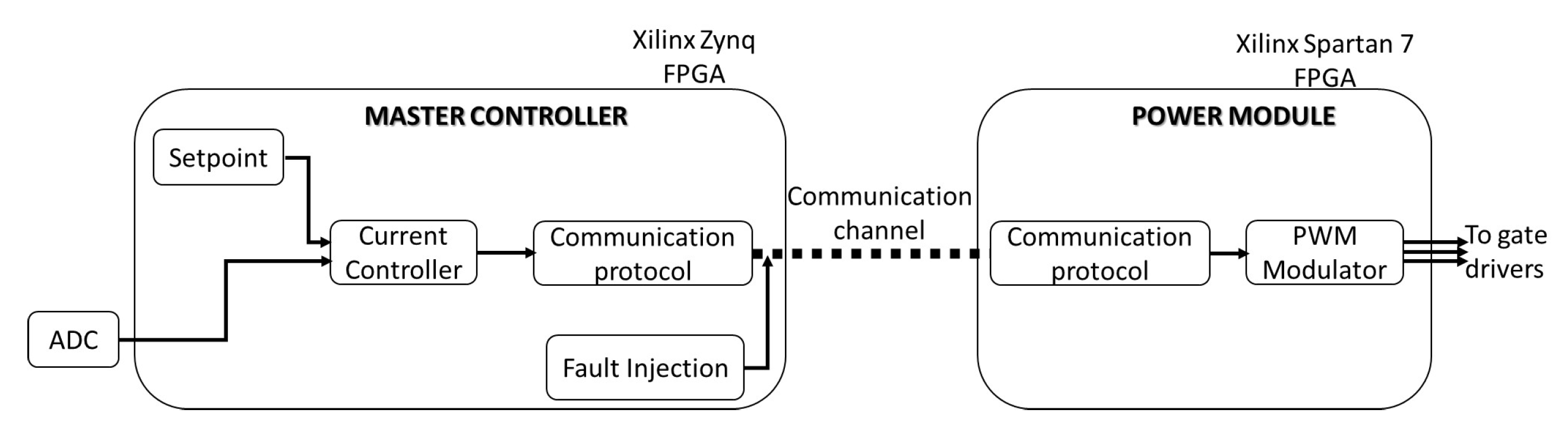
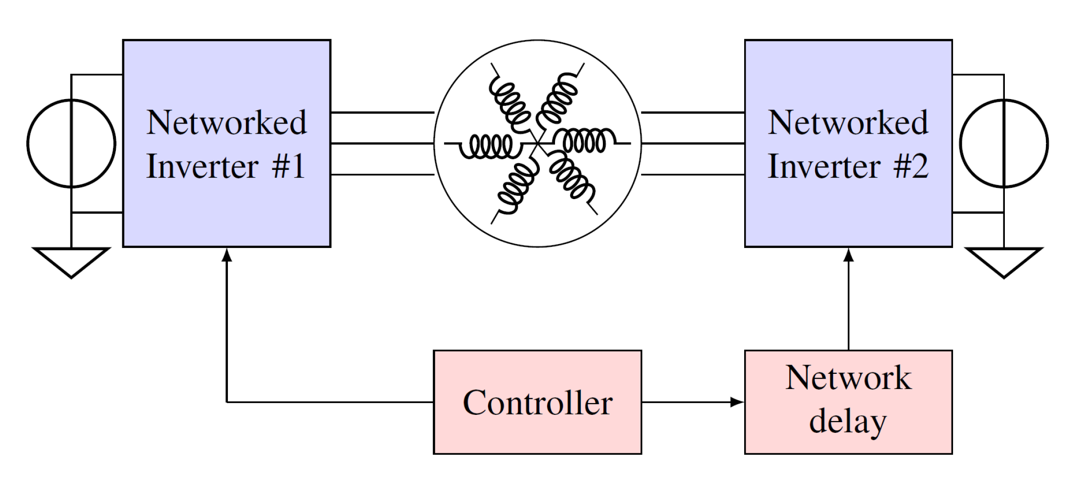
9]. The following paragraphs outline the technical choice that were made for the implementation on a FPGA. From a high level perspective, the system is composed of two parts: A master controller and one (or more) power module, as shown in 
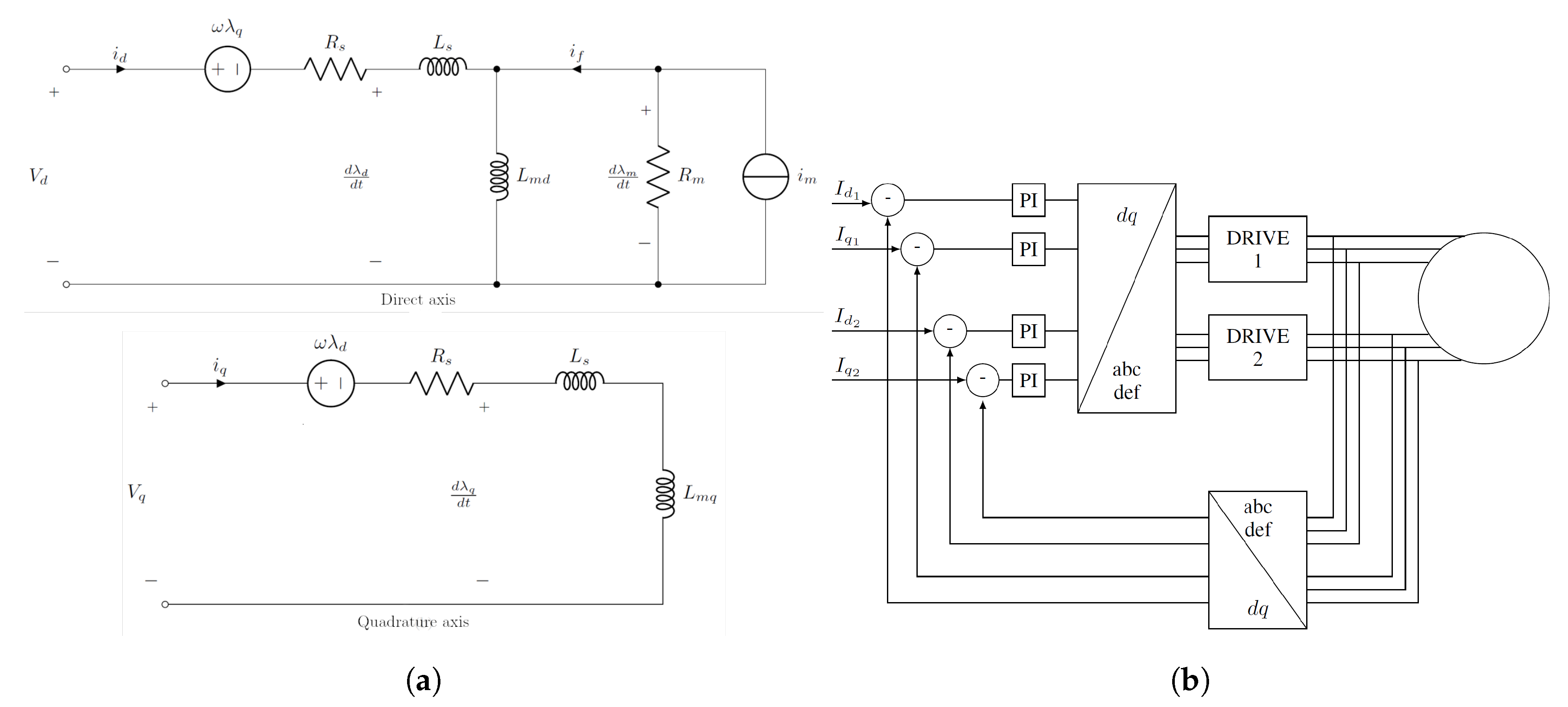
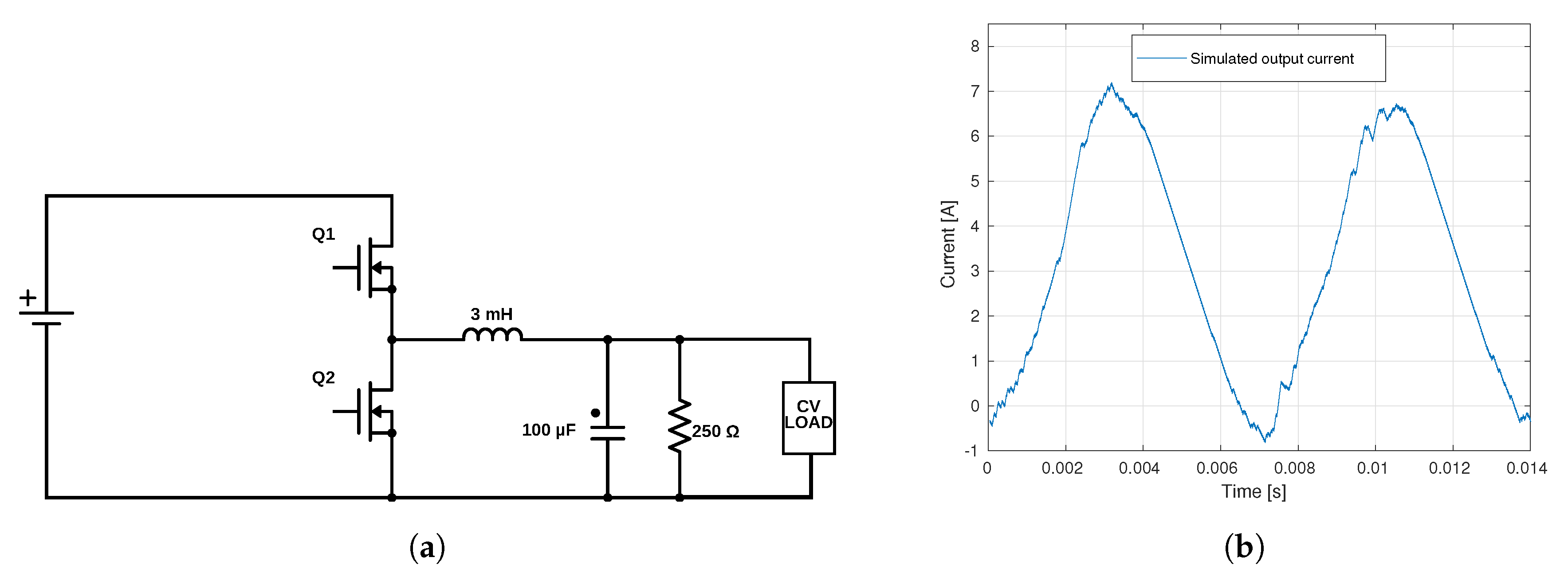
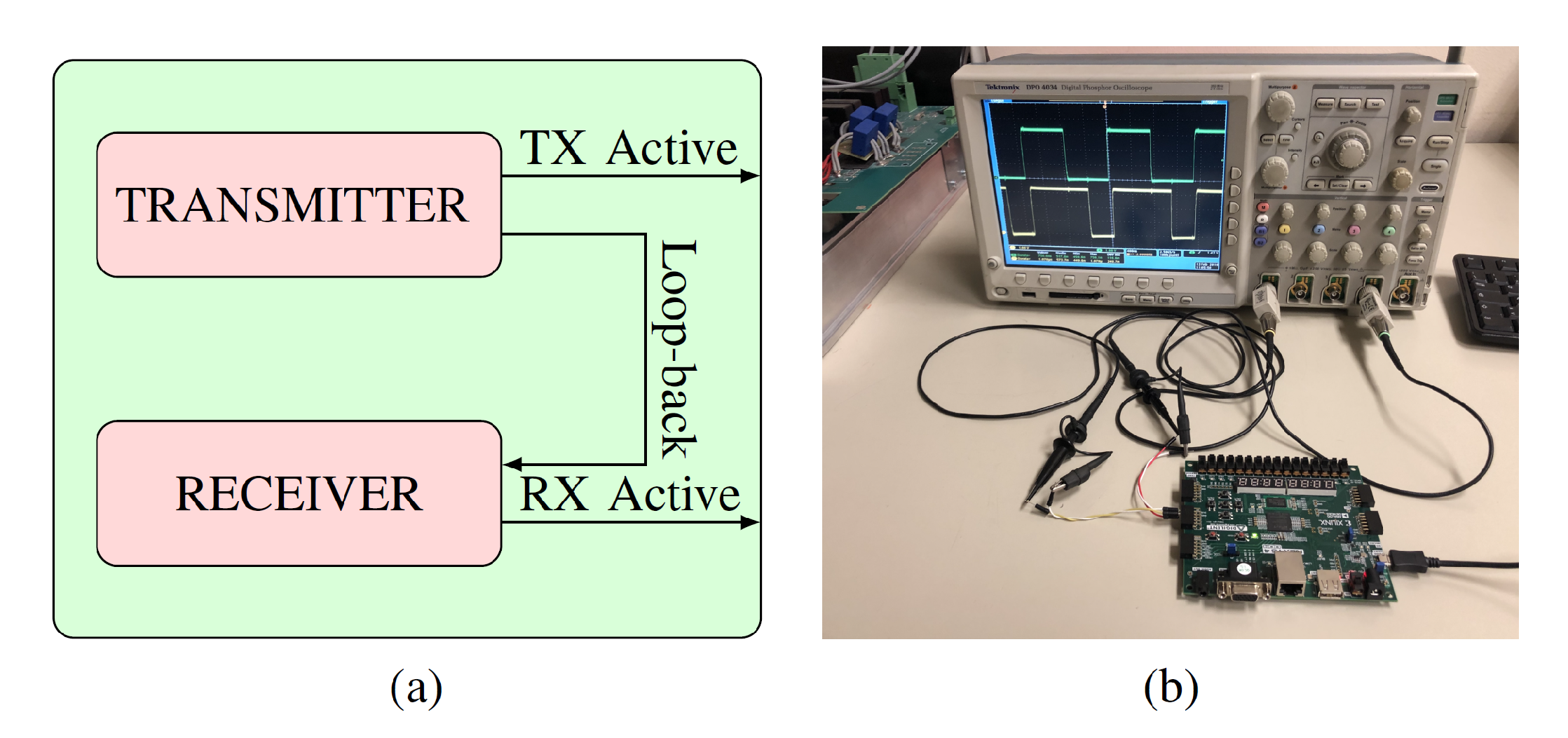
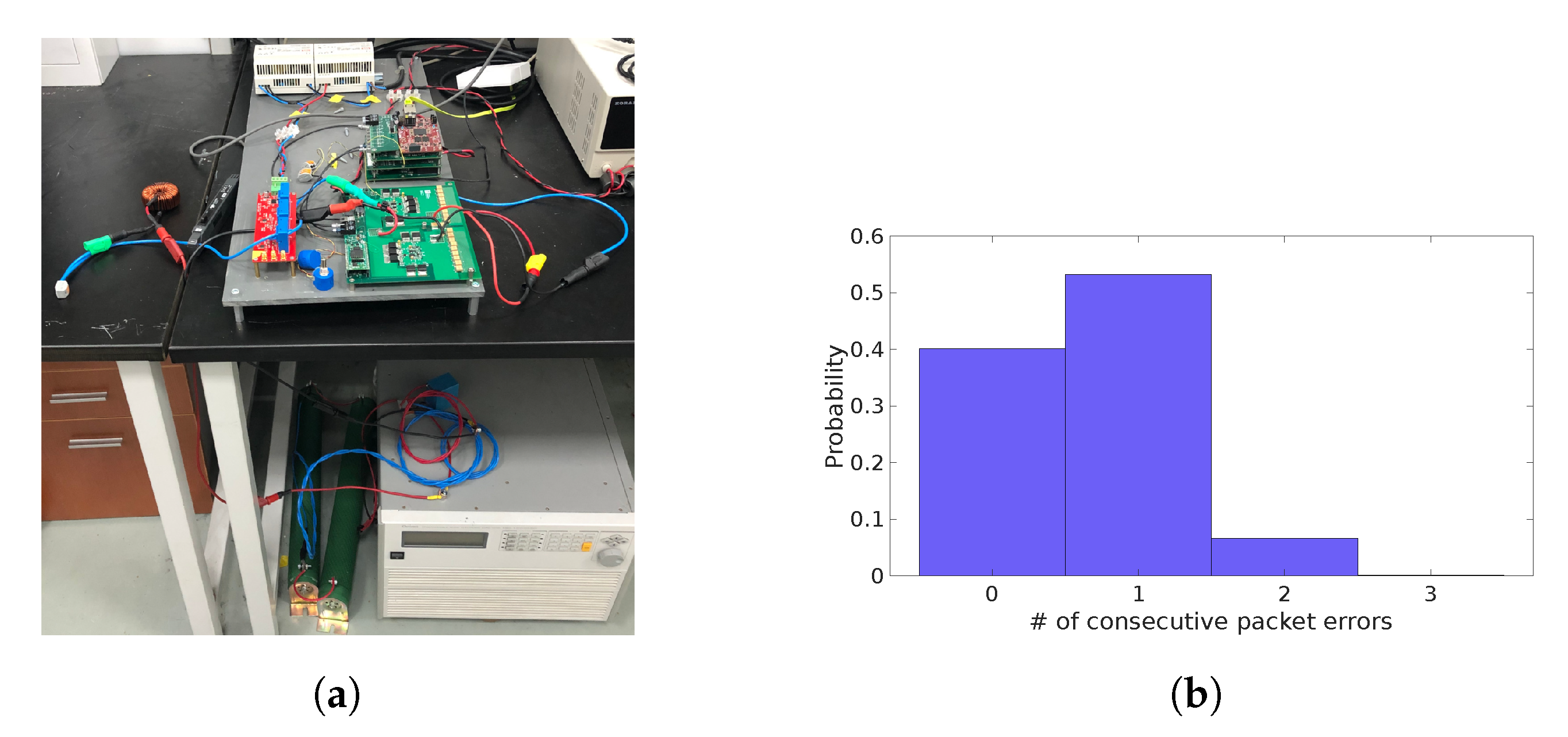
Figure 3. Both the master controller and power module are implemented on FPGA. The master controller exploits a Xilinx Zynq FPGA and is responsible for main control loop operations. It computes the control variables and send them to the power modules for its correct operation. Moreover, it measures the actual output current through an external ADC (Analog to Digital Converter) and compute the relevant duty cycles to be transmitted to the power module. For testing purposes, a fault injection module has been added to the implementation of the master controller. Before the communication signal is transmitted, some network errors are added in order to simulate the not ideal situation repeatably. The power module is implemented on a Xilinx Spartan 7 FPGA. In addition to the communication device needed to receive the appropriate instructions from the main controller, it generates the relevant PWM (Pulse Width Modulation) signals to control an external traditional buck converter. The communication blocks embedded on master and power modules follow the protocol described in Section 2. To evaluate the impact of different FEC techniques, two versions of the coder-decoder have been implemented and tested. In the following paragraph, the two solutions, based on the Hamming and RS algorithm respectively, are detailed.

3.1. Hamming Code

The designed Hamming encoder has to calculate the m H parity bits along with the global message checksum. To do this the payload needs to be modulo-2 multiplied by the generator matrix (often denoted with G). This matrix, when well chosen, will be fairly sparse, leading to a relatively simple set of multiple input exclusive or gates, whose implementation poses very few timing and area consumption problems. On the other hand, the global message checksum calculation, requiring very low computational power, results in gates with a large fan-in that can have a significant negative impact on timing. It is thus beneficial to split this operation into several smaller steps. The optimal partitioning choice is highly dependent on the underlying hardware architecture, however a simple two-stage pipeline is selected, as a balanced trade-off between area utilization and timing margins.
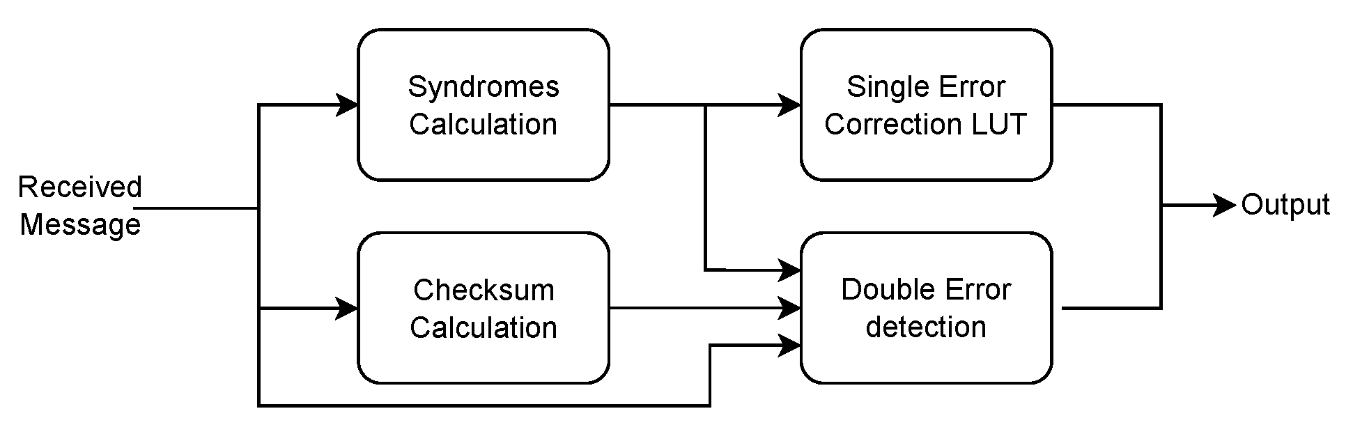
The traditional algorithm employed with Hamming encoded data is based on the principle of syndrome decoding. The m H bits “syndrome” is calculated, by multiplying (modulo-2) the received code-word by the parity check matrix (usually denoted with H, obtained by calculating the inverse of the parity columns in the G matrix). The value of the syndrome is only dependent on the position of the wrong bit. The core of this decoder’s implementation, whose structure is shown in Figure 4, organized in a two-stage pipeline. In the first step the syndrome of the received message, and the overall checksum are calculated. In the next clock cycle, single errors are corrected by locating the incorrect bit using a RAM-based Look Up Table (LUT), addressed by the calculated syndrome. At the same time, checksums are compared to detect whether a two bit error has occurred. Depending on the output of these two blocks, the correct message is sent to the outputs or, in case of a double bit error, a flag is raised, allowing the controller to discard the message.
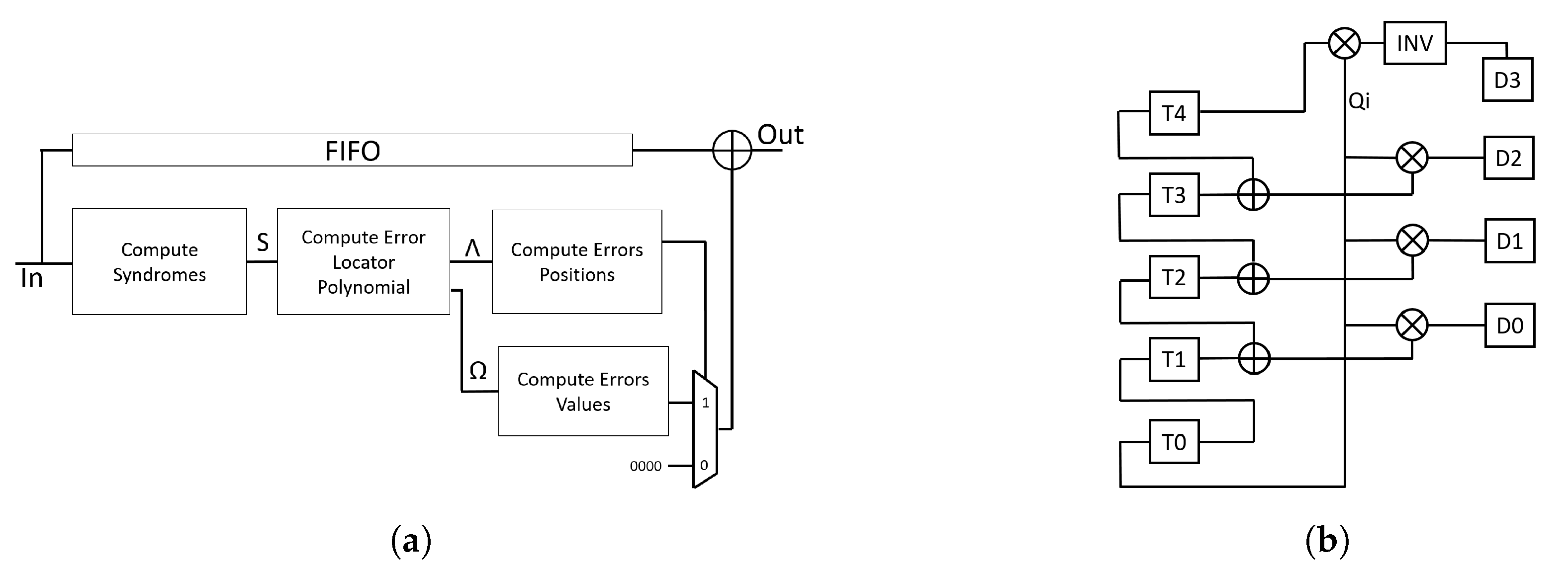
3.2. Reed-Solomon

The architecture of a RS encoder is based on a Linear Feedback Shift Register [22]. It consists of four GF multipliers and adders, and four 4-bit registers.
The general RS decoder architecture is depicted in Figure 5a. The syndrome block consists of 2t basic cell to compute syndromes symbols [23]. Since in a single cell the data is multiplied by a constant that represents a root of the generator polynomial, to limit the area occupation and speed up the operations, the Galois multiplier of the single cell has been replaced by a LUT. Moreover, thanks to the chosen generator polynomial the cell corresponding to the zero root of the polynomial does not need any multiplier. To compute Error Locator Polynomials the Euclidean algorithm is exploited [24]. The architecture for the Galois divider is shown in Figure 5b.
At the beginning, the registers T0-T4 are loaded with the divisor, while the dividend is stored in registers D3-D0. As the division proceed, the quotient and remainder of the division will be available in the T0-T4 registers. Depending on the degrees of the divisor polynomials and dividend, the remainder and quotient could have different degrees and therefore a different symbols number. A designed control logic deals with recognizing which of the T4-T0 symbols actually belong to the quotient or to the remainder. The designed divider is also able to handle the special case in which the most significant symbol of the syndrome is zero. Errors positions and values evaluation has been carried out with well-established Chien [25] and Forney [15,26] methods respectively. The whole designed architecture is, also in this case, pipe-lined.

3.3. Resource Usage

All the studied solutions have been implemented on a Xilinx XC7A100T Artix 7 family, with the Xilinx provided toolchain and common default settings and the resource usage relative to each design is consequently shown in Table 3. It is worth mentioning that these figures are highly dependent not only on the logic design but also on the underlying hardware architecture, toolchain used, optimization steps executed, and related parameter choice. The given figures should thus be examined in relation to each other. As already seen in the previous sections, there is high asymmetry between the encoder and decoder complexity. When comparing Hamming with the RS error correction algorithm, it is clear that the latter has a much higher complexity than the former. If these figures are normalized to the number of correctable errors, the cost for each correctable bit is much lower, making the RS Error Correction Code (ECC) very promising for application in this field. Lastly, when comparing the logic usages with respect to the capabilities of the FPGA’s in the Artix family, it is clear that the overall cost of even high performance error correction is quite low with a worst case usage of roughly 5 % (for the XC7A12T device).

4. Impact of Latency and Jitter on Control Performances

To show the impact of network-induced latencies and packet loss jitter, two different scenarios have been considered and simulated, the first is the control of a six-phase machine with two separate three phase drives with a networked central controller, the second scenario is a constant current output buck converter, that while extremely simple can be used both standalone, for battery charge operation, and as building block of many other topologies, used to implement smart transformers, like the dual active bridge.

4.1. Distributed Six-Phase Drive

To show the impact that the delay caused by a sub-optimal network connection can have on the performance of control loops in a real case application, the distributed drive system depicted in Figure 6 has been simulated. It consists of a symmetric star connected, six-phase, permanent magnet synchronous machine. To control the phase current, to which the torque is proportional, the machine phases are separated into two sets of three symmetrical phases, each one connected to a classical three-phases voltage source inverter. The outputs of the converters are directly managed by the networked master controller so that they can work together as a single unit. This architecture, when properly implemented, can grant a high degree of fault tolerance to the system. In case of single electrical failure to any of the components, the system can still carry on working, in three phase mode, provided a suitable derating factor is applied to avoid the windings thermal overload. The use of FPGA, as opposed to microcontrollers or DSPs, is one of the key enabling factors for the good performances of a similar system, as their greater flexibility allows the efficient implementation of customized fault tolerant peripherals.
The simplest, yet effective approach to the analysis and simulation of a six phase machine is its partition into two separate sets of three phase windings, that are shifted, relatively to each other, of π 3 radians. This allows the application of the standard rotating reference frame modelling techniques [27]. In simulation, the motor is represented by an equivalent circuit, shown in Figure 7a, that is derived from Equations (1)–(5) of the classical analytical model used for permanent magnet machines.
λ q = ( L s + L m q ) i q
λ d = ( L s + L m d ) i d + λ m
V q = d λ q d t + R s i q + ω λ d
V d = d λ d d t + R s i d ω λ q
T = 3 2 p ( λ d i q λ q i d )
The machines are driven by two classical voltage source inverters. A standard Piecewise Linear Simulator (PLECS) was used, where the transistors are replaced with idealized switching elements. This greatly reduces the simulation complexity, without any meaningful loss of precision, as the modelling of the switching transient while of critical importance when designing power electronics converters, is not as important to the dynamic performance of the whole system as their duration is negligible with respect to the whole period. To control the two inverters a standard field oriented control, shown in Figure 7b, is used, where a proportional-integral (PI) regulator is used to control the direct and quadrature currents, controlling thus the motor torque, as per Equation (5). The simulation parameters are listed in Table 4.
In this scenario, after a 0.15 s settling period, an intermittent delay is applied to the control signals of one of the two drives.
The introduction of a significant network delay impacts several key performance metrics’ drives. Firstly, the stability of the implemented control is significantly diminished, as large oscillations in both the direct and quadrature current are clearly present, with a peak to peak ripple amplitude as much as 1.7 times higher, as shown in Figure 8.
As shown, the addition of latency, be it network derived or otherwise, to a feedback control system can have an impact on several key performance indicators. However, the specific typology and magnitude of these effects is highly dependent on the specific control methodology and the parameters of the controlled system. In [28,29], a much more in-depth analysis of these phenomenons in two specific real world scenarios is presented. For these reasons, it is not possible to specify a typical or maximum allowed network latency, that can generally be valid for large classes of applications.

4.2. Constant Current Buck Converter

The considered hardware setup, shown in Figure 9a, is operated as a buck converter with syncronous rectification. In this scenario, a PI-based feedback control is used to keep constant the output current. To match the experimental setup described in Section 5, a low pass RC filter is also added in parallel to the load.
As with the previous simulation after an initial transient period where the network is allowed to run with no performance degradation and the control loops to stabilize, a randomized delay is added between the controller and power electronics models to represent to the network reception errors, with subsequent packet re-transmissions. The results are displayed in Figure 9b, showing a complete degradation of the system performance with large oscillations in the controlled output current.

5. Experimental Results

In order to validate the simulation results and demonstrate the potential of FEC techniques in power electronics communications, two different sets of experiments were carried out. The first, described in Section 5.1, seeks to validate the performance of the error correction algorithms and their implementation, in a wide variety of channel conditions. The second experiment has instead been designed to validate the simulation techniques and results, by replicating the setup described in Section 4.2.

5.1. Protocol Validation

To evaluate the performance of the studied error correction algorithms in the proposed application, it is of the utmost importance to identify the most relevant performance figures. In particular, it should not be taken for granted that these are the usual metrics typically used in Communication Engineering. The maximum achievable throughput, for example, while being crucial for high capacity channels, is of little use in control system where the amount of data to be transferred through the network is largely small when compared with the capabilities of modern communication channels, and thus easily transported even with spectral inefficient ECC techniques. By contrast the Bit Error Ratio (BER), as a measure of the coding robustness, is clearly applicable to the studied type of communications and will thus be evaluated in the following sections. However the most critical figure of merit for communications used in control systems is the latency, introduced, directly or indirectly, by the encoding and decoding processes, as it can impact the performance and stability of the control loops.
In Figure 10, the setup used in the experimental evaluation of the previously reported techniques is shown. The transmitter and receiver, containing the implemented FEC encoders and decoders, were implemented on the FPGA, with an internal loopback channel, whose operating frequency was chosen as 100 MHz (the maximum FPGA frequency). The duration of the transmit and receive operations was measured through signals (TX and RX active) outputted by the FPGA, and captured with an oscilloscope. To evaluate the BER, the transmitter sent through the channel a statistically significant sample of packets derived from a pseudorandom binary sequence introducing errors in randomly pre-determined locations. The data were then stored in a RAM block and collected at the end of each test for later analysis. The errors to be introduced were chosen in accordance with a Binary Simmetrical Channel (BSC), whose error probability was swept between 1 × 10 4 and 1 × 10 2 .

5.1.1. Latency

The results for the latency testing are shown in Table 5. In the second column, the absolute value added by the transmitter and receiver is represented, while the third column shows the increase of latency value with respect to a baseline value measured without FEC. In most situations, an unprotected communication strategy, while having a minimal impact on the control performance, is considered too unreliable to be viable, requiring ideal channel conditions. When comparing the Hamming coding with the RS, the increase in communication channel reliability is offset by a large total added latency. This, while rather large, with a measured value of 910 ns, is fixed, known, and stable. Hence, it is possible to evaluate the sensibility of the control loop during the design phase, allowing the eventual corrective measures to be adopted. The added delay for the Hamming coding is even lower, and at only 200 ns its impact is low enough for this technique to be directly applicable to most power electronics control architectures. For systems with particular requirements in terms of extremely wide control bandwidth or minimal latencies, further techniques for the characterization and compensation of the network latencies are available from modern control theory [28]. However, it is worth noting that by comparing these results with others achieved by similar works [16], the measured latency, even in the case of the RS code, was significantly lower. Hence, these results indicate a viable solution in this kind of application.

5.1.2. Evaluation of the Bit Error Ratio (BER)

To evaluate the robustness of studied error correction algorithms, the BER is calculated as in Equation (6)
B E R = N e r r o r s N t x b i t s
where N e r r o r s is the number of errors after error correction, and N t x b i t s is the number of total sent bits. To this purpose, a BSC was used as it can accurately model the conditions that can be found in the real world for power electronics systems [30]. The very simple fully digital hardware receiver architecture is incapable of any kind of error detection, apart from a complete channel failure, and thus the only possible type of error are bit flips. Burst errors are also not considered, as the wide-band noise typically present in solid state energy conversion systems is unlikely to corrupt a significant number of consecutive bits, and also taking into account the fairly low frequencies involved.
In Figure 11 the measured BER is plotted against the error probability for a BSC channel. This test clearly shows the relative error correcting capabilities of the various error correcting codes. As with the previous test, the results were shown for the two studied FEC techniques, together with the BER for the naked transmission when no error correction was used, as a baseline for the comparison. As expected, the RS coding had better performances across the whole range of channel conditions, however the gap between it and the simpler Hamming coding reduced significantly as the error probability increased, indicating a low impact of the error correcting coding on the overall number of errors, in those situations.
It is worth noting that in both cases the BER with error correction was much lower than the one for the uncoded channel, proving the efficacy of FEC even when overwhelmed with more errors than it could handle. For channels with very high error probabilities (due to poor SNR) the small gap between the two coding methods and relatively large latency of the stronger one, decreased the suitability of RS coding, requiring either a stronger coding, or a change in the physical channel design.

5.2. System Level Experimental Results

To validate the performed simulations, the setup, shown in Section 4.2, was built and tested. Here, the synchronous buck converter, fed by an Agilent N8955 power supply was used to step down the voltage, feeding a constant voltage load, emulated through the use of a Chroma 63804 programmable electronic load, with a constant current. To avoid issues stemming from the interaction between the electronic load internal control loops and the fast dynamics of the tested converter, a RC lowpass filter was also added in parallel with the load. Its inclusion did not change the overall system behavior, as most of the real loads, such as batteries or the power grid when the studied circuit was used as a part of a more complex converter topology, had a larger impedance at high frequencies. This led to a natural low pass response of the overall system. The parameter used in the experimental setup are shown in Table 6.
Two tests were carried out with the setup shown in Figure 12a, without and with network-related jitter caused by errors in the communication channel. In order to conduct a fair experiment, the same random pattern of errors was used in both tests, with the distribution shown in Figure 12b.
When the communication protocol was not designed to avoid network jitter (e.g., in the case of re-transmission requests), the feedback control was unstable. In Figure 13a, such a situation is presented. In this case, about half of the messages were delivered correctly and in time, but large oscillations with peaks up to 1.5 times the nominal output current value and a mean load current that was only half of the desired set-point were detected.
In Figure 13b instead, FEC is used to ensure correctness of the data received. This allowed the control system to work as intended, regulating the output current to the desired set-point and avoiding oscillations. The same output waveform was obtained with both Hamming and RS techniques, as long as the most appropriate was chosen to prevent the network jitter, according to the expected channel conditions the use of FEC allowed the compensation for transmission errors, thus allowing the control system to achieve a tight regulation of the output current to match the desired set-point, avoiding any oscillation.

6. Conclusions

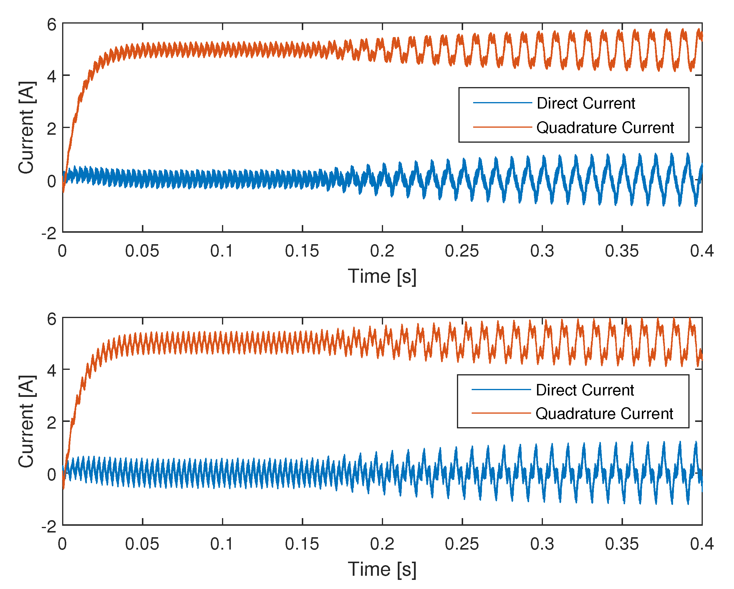
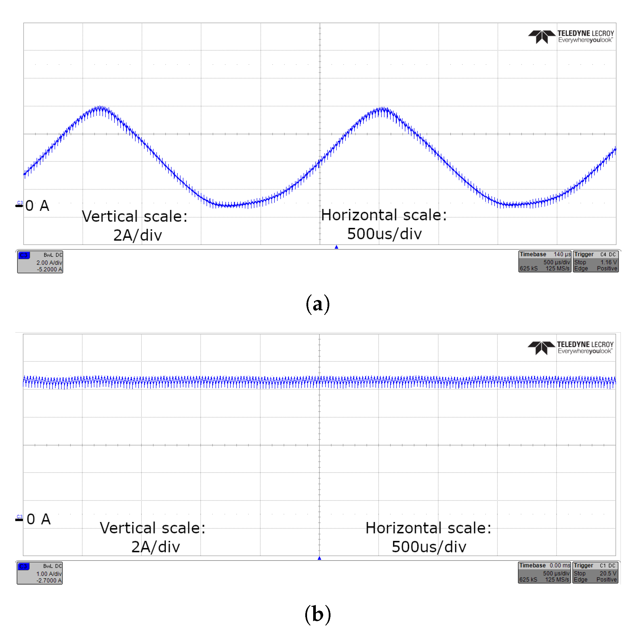
This paper showed how the performance and viability of distributed power electronics controls is highly dependent on the network performance. In particular, in non-ideal channel conditions, when reception errors are possible, the common detect and re-transmit strategy, while ensuring correctness of the data stream, could introduce jitter in the control loop, ultimately leading to instability. In fact, this constituted a time varying delay placed in the direct path of the control loop and it worsened the overall phase margin, potentially leading to oscillation. This phenomenon was proven by the simulations and then confirmed through experimental validations.
The introduction of FEC techniques to the communication between the master controller and the slave power modules, on the other hand, could still ensure an error-free data stream, while avoiding the introduction of any random jitter in the communication, thus proving to be the ideal method for distributed power electronics systems. The complementary switching transistor pairs were connected only to the PWM generator, whose duty-cycle was controlled by the rest of the system. Hence, the hardware of the slave power modules was affected only in an indirect way by the introduction of FEC. Two different FEC coding were evaluated and the performance of the proposed communication strategy was experimentally validated. A latency of 910 ns and of 200 ns were measured in the case of RS and Hamming code techniques, respectively. Both these results were comparable or even better than those presented in the state-of-the-art [16]. It is worth noting that the RS solution had better performances in terms of BER regardless of the channel conditions. However, the choice of which technique should be preferred must be made considering the characteristics of the specific application and installation (e.g., physical layout of the system, EMC immunity of the communication physical layer, dynamics of the overall system including load and power supply, etc.). Independently, on the specific application, it was proven that both RS and Hamming code improved the power control, deleting the oscillations that were visible in case of simple re-transmission requests when errors occurred in the communication.

Author Contributions

Conceptualization, V.B., F.S., I.D.M., D.B., G.B., G.F.; Methodology, V.B., F.S.; Validation, V.B., F.S.; Investigation, V.B., F.S.; Data Curation, V.B., F.S.; Writing—Original Draft Preparation, V.B., F.S.; Writing—Review and Editing, V.B., F.S., I.D.M., D.B., G.B., G.F.,; Visualization, V.B., F.S., I.D.M., D.B., G.B., G.F.; Supervision, I.D.M, D.B., G.B., G.F. All authors have read and agreed to the published version of the manuscript.

Funding

This research received no external funding.

Conflicts of Interest

The authors declare no conflict of interest.

References

  1. Zou, Z.; De Carne, G.; Buticchi, G.; Liserre, M. Smart Transformer-Fed Variable Frequency Distribution Grid. IEEE Trans. Ind. Electron. 2018, 65, 749–759. [Google Scholar] [CrossRef]
  2. Zou, Z.; Buticchi, G.; Liserre, M. Analysis and Stabilization of a Smart Transformer-Fed Grid. IEEE Trans. Ind. Electron. 2018, 65, 1325–1335. [Google Scholar] [CrossRef]
  3. Reimers, J.; Dorn-Gomba, L.; Mak, C.; Emadi, A. Automotive Traction Inverters: Current Status and Future Trends. IEEE Trans. Veh. Technol. 2019, 68, 3337–3350. [Google Scholar] [CrossRef]
  4. Buticchi, G.; Gerada, D.; Alberti, L.; Galea, M.; Wheeler, P.; Bozhko, S.; Peresada, S.; Zhang, H.; Zhang, C.; Gerada, C. Challenges of the Optimization of a High-Speed Induction Machine for Naval Applications. Energies 2019, 12, 2431. [Google Scholar] [CrossRef] [Green Version]
  5. Kim, M.; Lee, S.G.; Bae, S. Decentralized Power Management for Electrical Power Systems in More Electric Aircrafts. Electronics 2018, 7, 187. [Google Scholar] [CrossRef] [Green Version]
  6. Galassini, A.; Costabeber, A.; Gerada, C.; Buticchi, G.; Barater, D. A Modular Speed-Drooped System for High Reliability Integrated Modular Motor Drives. IEEE Trans. Ind. Appl. 2016, 1. [Google Scholar] [CrossRef]
  7. Aghaee, F.; Mahdian Dehkordi, N.; Bayati, N.; Hajizadeh, A. Distributed Control Methods and Impact of Communication Failure in AC Microgrids: A Comparative Review. Electronics 2019, 8, 1265. [Google Scholar] [CrossRef] [Green Version]
  8. Kojima, S.; Ishioka, T.; Yokoyama, T. A study of communication system for power electronics controller using FPGA based hardware controller. In Proceedings of the 2010 International Power Electronics Conference—ECCE ASIA, Sapporo, Japan, 21–24 June 2010; pp. 1262–1267. [Google Scholar] [CrossRef]
  9. Francis, G.; Burgos, R.; Wang, F.; Boroyevich, D. A power electronics communication protocol for distributed digital control architectures. In Proceedings of the 2008 IEEE Power and Energy Society General Meeting—Conversion and Delivery of Electrical Energy in the 21st Century, Pittsburgh, PA, USA, 20–24 July 2008; pp. 1–8. [Google Scholar] [CrossRef]
  10. Hashmi, K.; Khan, M.; Xu, J.; Shahid, M.; Habib, S.; Faiz, M.; Tang, H. A Quasi-average estimation aided hierarchical control scheme for power electronics-based islanded microgrids. Electronics 2019, 8, 39. [Google Scholar] [CrossRef] [Green Version]
  11. Li, W.; Wang, Z.; Jafarkhani, H. Repairing Reed-Solomon Codes Over GF(2). IEEE Commun. Lett. 2020, 24, 34–37. [Google Scholar] [CrossRef]
  12. Van Waes, J.; Lannoo, J.; Vankeirsbilck, J.; Degraeve, A.; Peuteman, J.; Vanoost, D.; Pissoort, D.; Boydens, J. Effectiveness of Hamming Single Error Correction Codes Under Harsh Electromagnetic Disturbances. In Proceedings of the 2018 International Symposium on Electromagnetic Compatibility (EMC EUROPE), Amsterdam, The Netherlands, 27–30 August 2018; pp. 271–276. [Google Scholar] [CrossRef]
  13. Karim, Y.A.; Sarr, N.B.; El-Qachchach, I.; Cances, J.; Meghdadi, V.; Boeglen, H.; Vauzelle, R. Performance of rank metric codes for interference constrained wireless sensor networks. IET Wirel. Sens. Syst. 2018, 8, 215–222. [Google Scholar] [CrossRef]
  14. Eleruja, S.; Abdu-Aguye, U.; Ambroze, M.; Tomlinson, M.; Zak, M. Design of binary LDPC codes for Slepian-Wolf coding of correlated information sources. In Proceedings of the 2017 IEEE Global Conference on Signal and Information Processing (GlobalSIP), Montreal, QC, Canada, 14–16 November 2017; pp. 1120–1124. [Google Scholar] [CrossRef]
  15. Bianchi, V.; Bassoli, M.; De Munari, I. Comparison of FPGA and Microcontroller Implementations of an Innovative Method for Error Magnitude Evaluation in Reed Solomon Codes. Electronics 2020, 9, 89. [Google Scholar] [CrossRef] [Green Version]
  16. Savio, P.; Varatharajan, A.; Vizzaccaro, E.; Abdelfattah, S.; Franco, G.; Abrate, S.; Pellegrino, G.; Curri, V. Control of Power Electronics through a Photonic Bus: Feasibility and Prospects. J. Sens. Actuation Netw. 2018, 7, 53. [Google Scholar] [CrossRef] [Green Version]
  17. Chang, S.; Kelley, B. An Efficient Time Synchronization Scheme for Broadband Two-Way Relaying Networks Based on Physical-Layer Network Coding. IEEE Commun. Lett. 2012, 16, 1416–1419. [Google Scholar] [CrossRef]
  18. Arazi, B. Self Synchronizing Digital Scramblers. IEEE Trans. Commun. 1977, 25, 1505–1507. [Google Scholar] [CrossRef]
  19. Witzke, K.; Leung, C. A Comparison of Some Error Detecting CRC Code Standards. IEEE Trans. Commun. 1985, 33, 996–998. [Google Scholar] [CrossRef]
  20. Hamming, R.W. Error detecting and error correcting codes. Bell Syst. Tech. J. 1950, 29, 147–160. [Google Scholar] [CrossRef]
  21. Reed, I.S.; Solomon, G. Polynomial Codes Over Certain Finite Fields. J. Soc. Ind. Appl. Math. 1960, 8, 300–304. [Google Scholar] [CrossRef]
  22. Berlekamp, E. Bit-serial Reed—Solomon encoders. IEEE Trans. Inf. Theory 1982, 28, 869–874. [Google Scholar] [CrossRef]
  23. Huynh, R.; Ge, N.; Yang, H. A low power error detection in the syndrome calculator block for reed-solomon codes: RS(204,188). Tsinghua Sci. Technol. 2009, 14, 474–477. [Google Scholar] [CrossRef]
  24. Sugiyama, Y.; Kasahara, M.; Hirasawa, S.; Namekawa, T. A method for solving key equation for decoding goppa codes. Inf. Control 1975, 27, 87–99. [Google Scholar] [CrossRef] [Green Version]
  25. Lee, H.; Lee, Y.; Yangand, H. Implementation of the Chien search algorithm on application specific instruction set processor. In Proceedings of the 2012 IEEE International Conference on Consumer Electronics (ICCE), Las Vegas, NV, USA, 13–16 January 2012; pp. 183–184. [Google Scholar] [CrossRef]
  26. Forney, G. On decoding BCH codes. IEEE Trans. Inf. Theory 1965, 11, 549–557. [Google Scholar] [CrossRef]
  27. Lipo, T. A Cartesian Vector Approach to Reference Frame Theory of AC Machines. In Proceedings of the International Conference on Electrical Machines, Lausanne, Switzerland, 18–24 September 1984; Volume 1, pp. 239–242. [Google Scholar]
  28. Geelen, W.; Antunes, D.; Voeten, J.P.M.; Schiffelers, R.R.H.; Heemels, W.P.M.H. The Impact of Deadline Misses on the Control Performance of High-End Motion Control Systems. IEEE Trans. Ind. Electron. 2016, 63, 1218–1229. [Google Scholar] [CrossRef] [Green Version]
  29. Dai, J.; Phulpin, Y.; Sarlette, A.; Ernst, D. Impact of delays on a consensus-based primary frequency control scheme for AC systems connected by a multi-terminal HVDC grid. In Proceedings of the 2010 IREP Symposium Bulk Power System Dynamics and Control—VIII (IREP), Rio de Janeiro, Brazil, 1–6 August 2010; pp. 1–9. [Google Scholar] [CrossRef] [Green Version]
  30. Maxino, T.C.; Koopman, P.J. The Effectiveness of Checksums for Embedded Control Networks. IEEE Trans. Dependable Secur. Comput. 2009, 6, 59–72. [Google Scholar] [CrossRef]
Figure 1. Different modular drive configurations: (a) Single Inverter; (b) Direct Gate driving; and (c) Distributed Gate Driving solid lines represent direct gate connections, dashed arrows represent communication channels).
Electronics 09 00281 g001
Figure 2. Diagram of the overall communication chain.
Electronics 09 00281 g002
Figure 3. Schematic view of the implemented system.
Electronics 09 00281 g003
Figure 4. Architecture of the Field Programmable Gate Arrays (FPGA) implementation of the Hamming decoder.
Electronics 09 00281 g004
Figure 5. (a) Architecture of the FPGA implementation of the RS Decoder and (b) architecture of the implemented 4-bits Galois Field (GF) Divider.
Electronics 09 00281 g005
Figure 6. Delay impact evaluation simulation setup.
Electronics 09 00281 g006
Figure 7. (a) Rotating reference frame equivalent circuits of the studied machine and (b) diagram of the employed control scheme.
Electronics 09 00281 g007
Figure 8. Direct and quadrature currents: for networked drive 1 and for networked drive 2.
Electronics 09 00281 g008
Figure 9. (a) Syncronous current output buck converter and (b) steady state converter output current.
Electronics 09 00281 g009
Figure 10. Experimental setup: Diagram of hardware implemented in FPGA (a) and picture of the experimental setup (b).
Electronics 09 00281 g010
Figure 11. BER (Bit Error Ratio) as a function of error probability for a BSC (Binary Simmetrical Channel) channel.
Electronics 09 00281 g011
Figure 12. (a) Experimental setup and (b) packet error distribution used in the tests.
Electronics 09 00281 g012
Figure 13. Output current waveforms, with (a) and without (b) network-induced jitter. The oscilloscope settings are as follows: 500 μs horizontal scale, 2 A/div, and 1 A/div.
Electronics 09 00281 g013
Table 1. Parameters of the studied Hamming code.
ParameterValue
m H 6 bits
k H 40 bits
Table 2. Parameters of the studied Reed–Solomon (RS) code.
ParameterValue
Primitive polynomial x 4 + x + 1
Generator polynomial ( x 1 ) ( x 2 ) ( x 4 ) ( x 8 )
m R S 4 bits
k R S 11 symbols
n R S 15 symbols
t R S 2 symbols
Table 3. Resource usage overview.
AlgorithmEncoder/DecoderTotal Usage
LUTRegistersLUTRegisters
NoneTX00102102
RX0067182
HammingTX2887139199
RX99128166438
Reed–SolomonTX6796244310
RX460541573710
Table 4. Simulation parameters.
ParameterValue
Switching frequency10 kHz
DC-link voltage600 V
Average output power1900 W
Injected delay1.5 μ s
Delay injection frequency100 Hz
Delay injection start time0.15 s
Table 5. Latency test results.
FEC
Technique
Absolute
Latency
( ns )
Relative
Latency
( ns )
Total Added
Latency
( ns )
NoneTX46000
RX4500
HammingTX54080200
RX570120
Reed–
Solomon
TX750290910
RX1070620
Table 6. Experimental results parameters.
Parameter NameValue
Switching frequency 40 k Hz
Supply voltage 70 V
Load voltage 25 V
Load current set-point 5 A

