1. Introduction
Since the past two decades, Distributed Energy Sources based on Renewable Energy have grabbed much attention in power transformation and distribution sectors. In particular, solar-photovoltaic (PV) systems have the highest growing rate (along with wind energy) with the addition of 109 GW in 2018–2019 [
1]. In terms of installed capacity, PV energy increased from 22 to 489 GW in this decade [
2]. The integration of solar energy to the utility grid requires power processing stages in order to successfully inject the gathered energy. The implementation of utility-scale solar systems requires galvanic isolation according to standards in many countries, and it is conventionally implemented by a grid frequency transformer. Even though traditional transformers are reliable and efficient, they are also heavy and bulky [
3].
Some approaches for PV systems propose the implementation of Medium-Frequency (MF) isolation in order to reduce volume and weight [
3,
4,
5]. The topologies with MF links usually features: a DC-AC stage consisting on a DC-DC converter and a DC-AC stage in order to drive the transformer, a Magnetic link operating in medium-high frequency, and an AC-AC stage consisting on a rectifier and a DC-AC stage. The key features of these systems are: individual maximum power point tracking (MPPT), galvanic isolation, enhanced voltage elevation ratio, reduced total harmonic distortion (THD), voltage stress reduction in medium-voltage (MV) stage, and reduced overall system volume and weight. Some drawbacks are: voltage imbalance in multilevel cells due to different power levels in each string, more power stages due to the presence of an additional low voltage inverter and MV rectifier, and increased stress in low voltage stage switches since the all the input power must be handled by a single switch. A solution for multilevel cell imbalance is presented in [
3] featuring a MF link that consists on a transformer with several secondary windings which being magnetically coupled
naturally balances the cascaded cells of the multilevel converter. Some downsides are that the system has four power stages, and reports low global efficiency levels. However, some adjustments in the topology can help improving reliability and efficiency. The PV system low voltage side in [
5] consists on a PV string and a DC-AC power stage. The DC-AC power stage requires buck-boost and MPPT capability. DC-AC stage is commonly integrated by a boost converter and an inverter in order to drive the MF transformer [
5]. Another approach is stated in [
6], proposing a flyback converter plus a H-bridge topology for DC-AC stage features, and enhanced efficiency with high frequency isolation; however, the number of semiconductors and current stress limits the topology to low power applications (<300 W). In [
7] a Cuk-SEPIC combination featuring a single switch and coupled inductors is presented in order to obtain a bipolar output enhancing efficiency, however current stressed switch can present reliability problems.
Since PV system behave as current sources, current-fed converters are considered for the DC-AC stage. The isolated current-fed push-pull converter features a low component count and simply circuitry which makes it rather reliable and simple to implement; it also benefits from a high-voltage conversion ratio [
8,
9,
10]. Some identified drawbacks of the topology are: high switching losses, high-voltage spikes in switches, high start-up current, and central tapped transformer coils requires a bigger core and can be a serious limitation for a magnetically coupled multiport configuration [
9,
11,
12,
13].
The L-type converter is an interesting topology that features reduced current stress in switches and reduced voltage stress on output capacitor and diodes [
8,
11]. There are a better use of the magnetic core of the MF link and thus making the topology a good option for the multiport implementation. Some limitations of the topology are: higher voltage efforts in switches, voltage spikes in switches due to a resonance with the leakage inductance of the transformer. Current-fed topologies with boost operation also require additional start-up circuitry due to the current in inductors during starting process. The L-type converter is suitable to low voltage, high current applications [
8,
11].
The Z-source inverter (ZSI) has been considered for DC-AC converters [
14,
15]; this topology has a buck-boost DC-AC capability in a single-stage which suggests an efficiency and reliability enhancement. The operation principle of the ZSI and current-fed topologies mentioned consist in apply a shoot-through state to overlap the H-bridge branches (0V) which provides natural protection against short-circuits, making it suitable for large-scale applications. After its presentation, variations on the topology were proposed for many applications such a grid-tied converters without galvanic isolation [
16,
17,
18], with galvanic isolation [
19,
20,
21], and finally for grid-tied PV systems [
22,
23,
24].
Z-sources topologies are interesting for PV applications because they can operate as voltage and current source. Additionally, Z-source converters operating as current source can be better applied in medium-high power applications due to the restriction of <1 kV in PV arrays terminals. A current fed Z-source Inverter (CZSI) version is proposed in [
25] which features a constant source current, protecting the PV array from returning current.
The CZSI shares many features of the above mentioned topologies such as DC-AC power processing in a single stage and voltage spikes in switches due to resonance with the leakage inductance [
12]. Some particular feature of the CZSI in deference to the mentioned topologies is a very low current stress in diode a capacitors, which are the most vulnerable elements on the Z network and thus enhancing the reliability of the circuit. Some drawbacks of the CZSI against the other topologies are the number of passive components and limited voltage boost. Since the PV system voltage does not presents a wide variation, voltage boost drawback is not considered of high relevance. The CZSI has similar to L-type topology power requirements for the magnetic core of the MF link, which is an important feature for multiport applications.
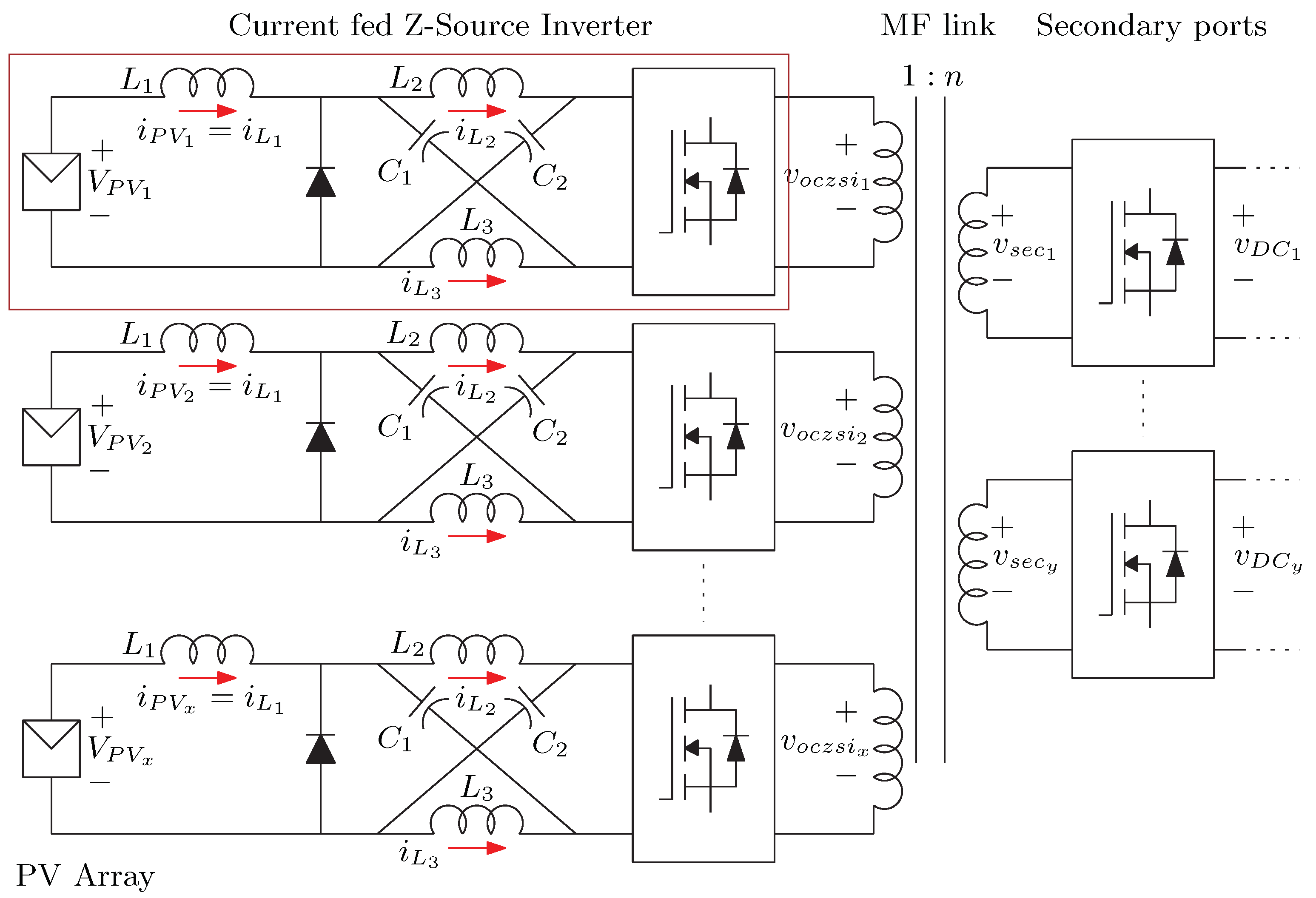
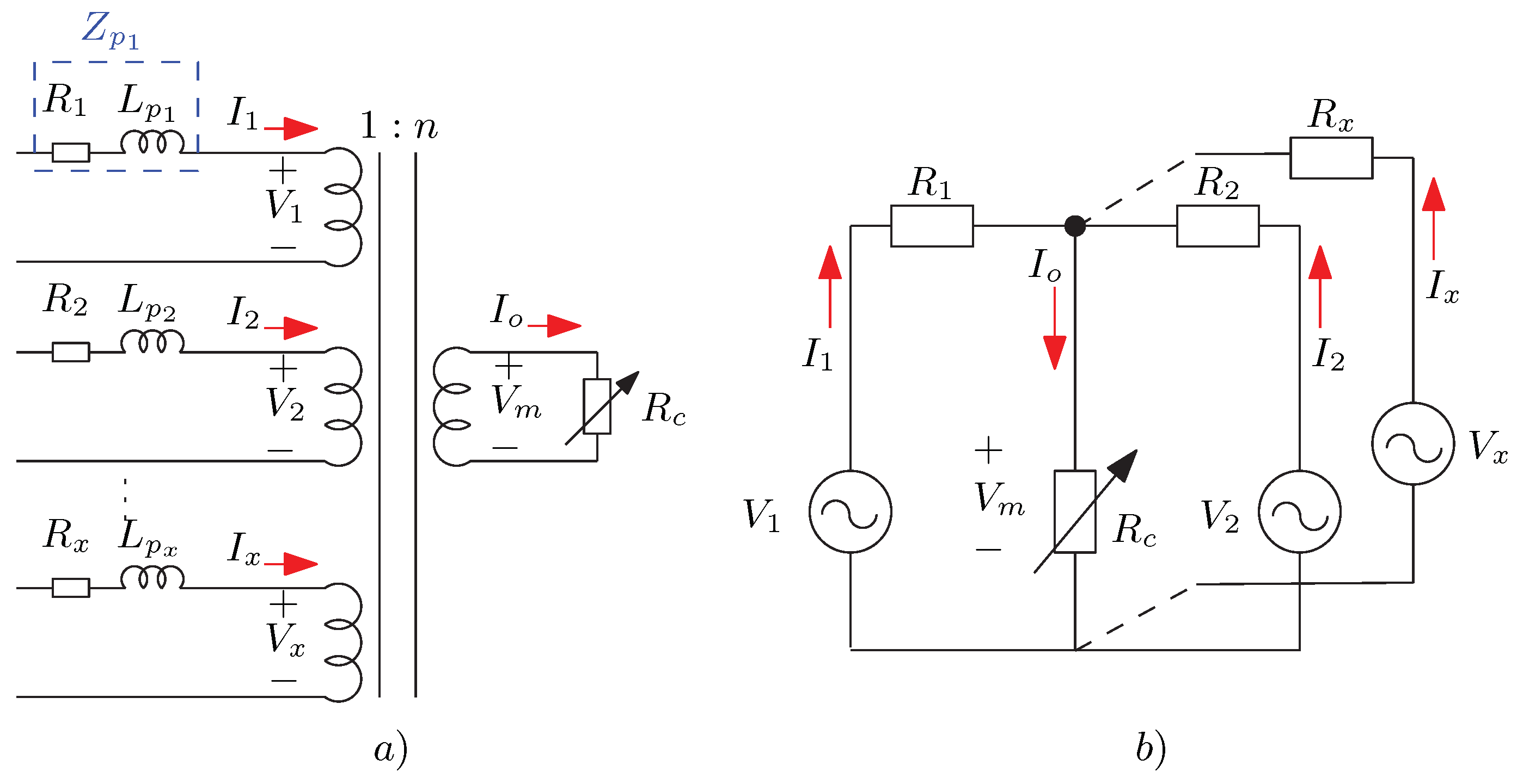
The system considered in this work is shown in
Figure 1 and consists in three power stages: Low voltage DC-AC stage consists in a PV array, followed by an elevation stage based on a current-fed Z-source inverter (CZSI) that performs MPPT and sets the voltage for the inverter who will drive the MF link; MF Link is an elevation AC-AC stage which provides multiport configuration integrated by multiple isolated and magnetically coupled inputs and outputs. The MF Link can manage
x primary ports and
y secondary ports, only restricted by the physical space and power the magnetic core of the transformer can handle. In this study, three input ports where selected since is the minimum number of modules in order to validate that different power levels can be processed in
x modules and not only flowing between two modules, and in order to show that output ports are balanced, two ports where selected.
The focus of this paper is derived from [
26] and presents the analysis of a multiport isolated link in asymmetrical input power transference conditions using CZSI modules to manage the energy. This work shows CZSI analysis, simulation and experimental results to validate the analysis performed. This proposal offers reduction of power stage by using CZSI modules energized by unbalanced PV systems, reliable magnetic isolation with a multiport link to meet standard requirements and, naturally balanced output ports and isolated sources for grid-connected oriented applications.
2. Current-Fed Z-Source Inverter Operation and Design
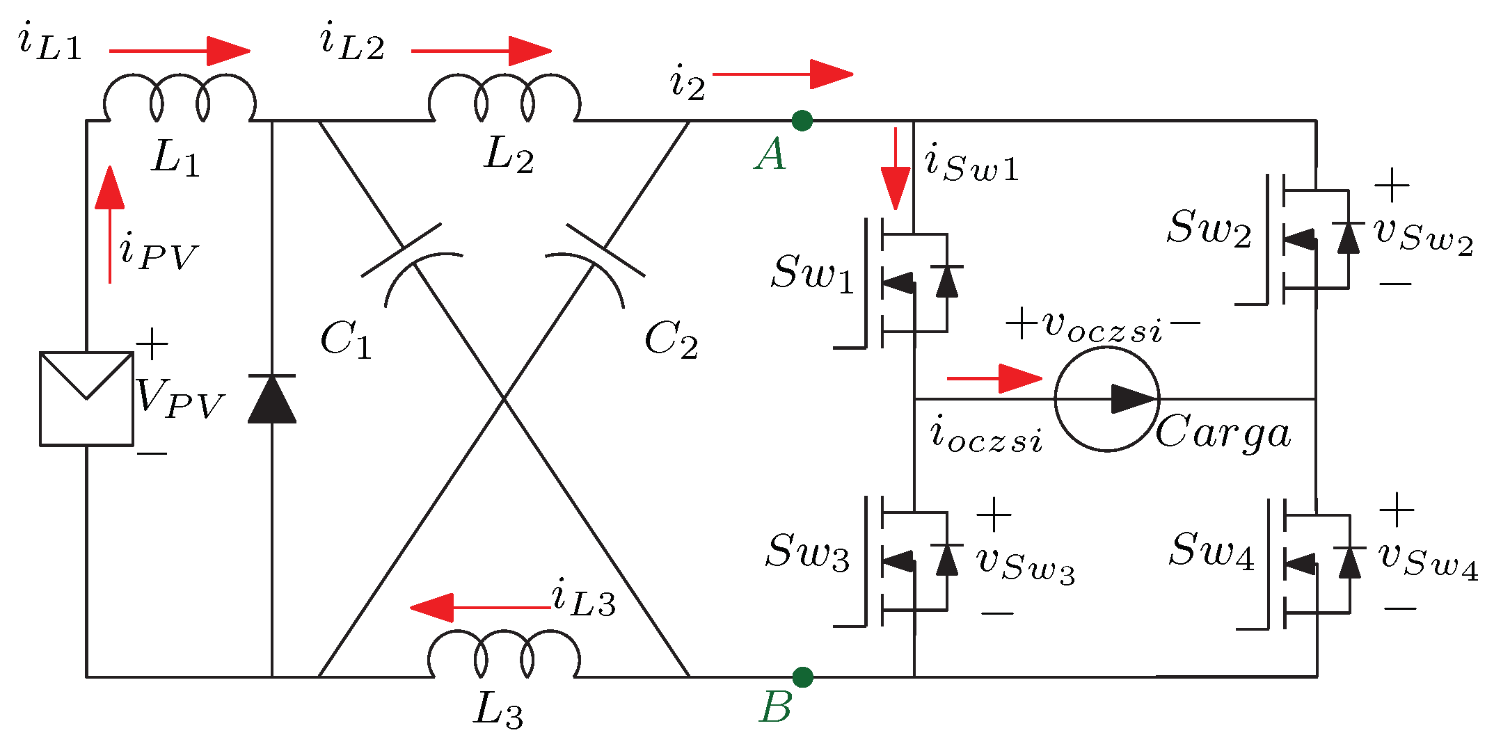
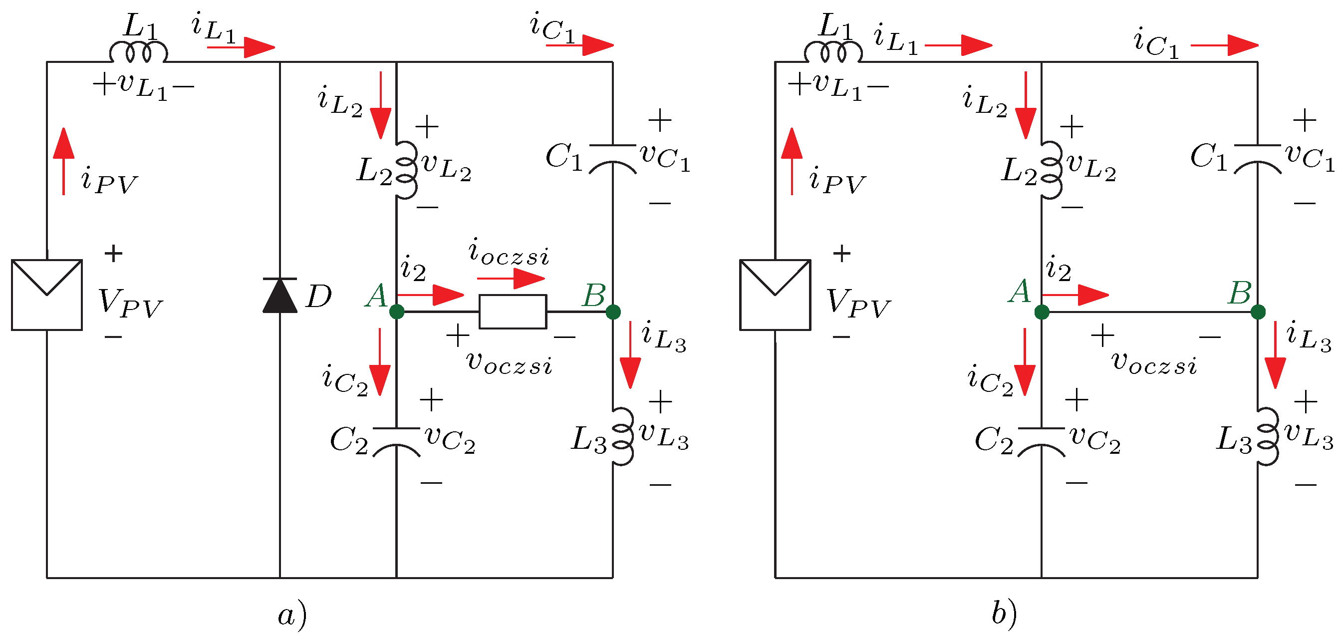
In
Figure 2, the CZSI circuit is presented and
Figure 3 shows the equivalent circuits for operation states. In steady state, average voltage in
,
and
remains zero as well as current in
and
over a switching period
T. The CZSI presents two main operation states: conduction and shoot-through; in conduction state mode (
and
ON and
and
OFF,
Figure 3a), current across inductors
,
and
is given by PV array
, and the voltage across the capacitors is set by the PV source
. During conduction state,
is charging with
, to supply current for the impedance network later.
In shoot-through state (All switches are ON,
Figure 3b),
and
rises as
falls since
supplies the current,
remains constant in
, limited by inductance
L. In this time, voltages in inductors are imposed by
. The capacitor voltage decrease in
and is limited by a capacitance
C. As it can be seen, that the Z LC circuit is always in conduction and the switches are the ones that control operation modes, an hence, the output voltage. The required shoot-through duty cycle
for a desired
can be found by the following expression:
where
is the peak value of
. The voltage boost for the CZSI is directly modified by
; therefore, by manipulating this duty cycle the MPPT can be performed and the DC-AC conversion remains in a single stage.
Output voltage can be obtained through Equation (
1), as it is a function of
; higher values of
produces higher gain limited to 2
.
RMS voltage is obtained by:
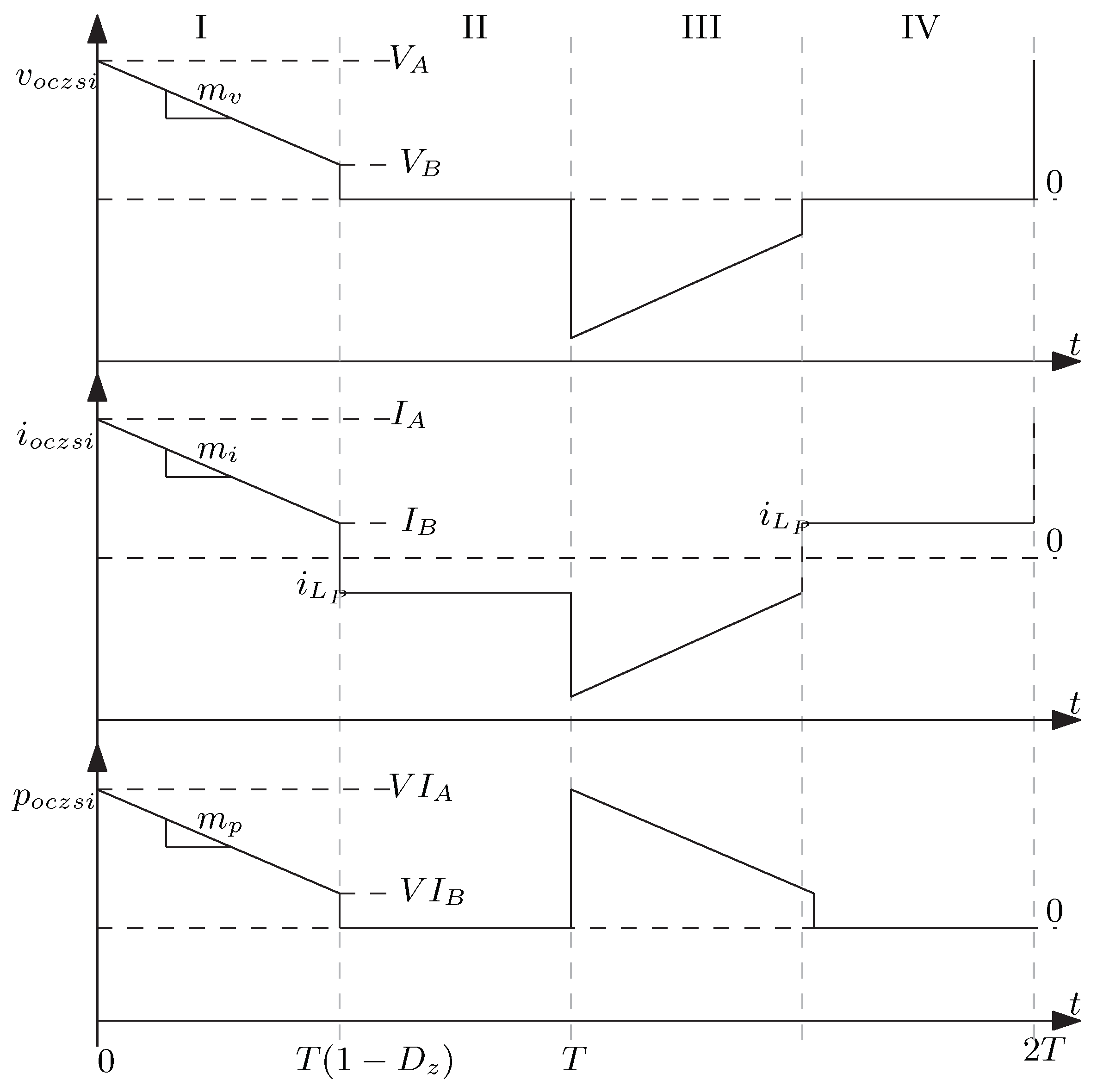
The shoot through time is shared by all of the modules due to the parallel connection, thus if one of the windings is in OV, the rest will be in OV as well. The last results in all of the windings sharing the duty cycle at the higher value.
The effect of
in switches is that during
, half of the current
given by:
is conducted by all switches. During
, current in switches is
. In conduction mode,
has a ripple
with a slope given by:
where
and
are peak values of
(
Figure 4). However,
is affected by winding impedance
Z composed by the leakage inductance
and the winding resistance, producing a non-zero current
(
Figure 4). The RMS current for
is given by:
By solving Equation (
5),
is given by:
where
is the upper
value,
the lower value, and
the leakage inductance.
In
Figure 5a, a simplified representation of a multiport configuration consisting on
x primary windings transformer and a single output is shown. Voltages
,
through
are the RMS value of CZSI modules output voltage
, and
is the secondary voltage
. In the MF link, the sum of average power supplied to each primary port must match the average power on the secondary ports, thus for a single output:
expanding the concept to
y secondary ports, the sum of the average power on each secondary output must also match the sum of the average input power:
For multilevel converters applications, it can be considered that power in each secondary port is balanced since they all have the same number of turns and the same output voltage. Secondary ports also share the same current since the all supply the same load, thereby Equation (
8) can be expressed as:
The parallel configuration shows that when a module is in shoot-through state, the remaining modules will share this state, thus voltage will be zero for all of the windings, resulting in an identical equivalent value for all input CZSI modules. The last implies that all the cells will have very similar values of .
The imposed duty cycle will be the higher value of all CZSI modules for the MPP, thus having different references is not necessary. Current levels will be in function of the power supplied by the PV array, thus different in all primary ports.
Despite the different power levels on the modules, the non-zero current associated to , remains similar for all windings since it is product of parasitic elements, and it is assumed that all windings are homogeneous.
Semiconductor Sizing for CZSI Modules
The voltage and current stress on semiconductors are defined by the operation mode of the CZSI module. The voltage stress for the semiconductors on CZSI conduction mode, is the voltage
and can be found with Equation (
1) and zero for shoot-through mode:
For selection purposes, a security factor of 50% can be added to
and is given by:
The current across the semiconductors, also depends on operation mode and can be expressed by:
The maximum current that semiconductors must conduct is the peak value of
plus a security factor of 25%. The current to be considered when choosing a device is given by:
3. Power Transfer under Unbalanced Conditions
An issue of having the whole installed capacity divided in strings is that the power in each array of PV panels can be unbalanced. Let’s consider a two input modules scenario, where and are CZSI modules output power and are different from each other.
A simple scheme is given in
Figure 5b for analysis purposes. Resistance
R is considered equal for all windings and thus
. From
Figure 5b, the voltage on the secondary side can be computed by:
where
n is the turn ratio and,
and
are the RMS values of
in modules 1 and 2 respectively. Such voltages cannot be arbitrary set to extract two different power levels on each loop, since (
14) has to be fulfilled. If the voltage
is imposed, then
will be in function of the desired power, thus
is a variable voltage source. To find a combination of
and
, that will allow different power transfer on modules, first
must be found in terms of
with (
14). Then
can be computed from:
By solving (
15) for
, a voltage value for
to transfer
can be found. For more than two modules or windings, a similar analysis can be performed. One module has a fixed voltage, and all the subsequent modules adapt their voltage to meet the power transference needed.
Therefore the current for
x given modules, (
17) can be solved for
:
Once expressions for output voltage and current are given, power on each winding can be calculated. Based on
Figure 4, the average power is given by:
where
and
are the upper and lower
values respectively. Apparent power S is expressed by:
From (
20) it can be observed that the
component is associated to reactive power, and since all cells have similar values of
(because all windings are identical) the component in
will be the same for all modules, an thus, have similar reactive power levels on all cells despite power level.
4. Results
Once the operation principle has been presented and the design equations given, simulation studies in PSIM, and experimental tests were performed with the parameters shown in
Table 1. Simulations were performed considering the schematic in
Figure 1; a PV system with a MF link including 3 primary ports and 2 secondary ports with a turn ratio of 1:7. A variable DC load is applied to each secondary port in order to extract 300 W from each PV array to get a total output power of 900 W, also, each CZSI module has a switching frequency ok 20 kHz with an input voltage of 50 V.
After the validation through simulations, a prototype has been built. The experimental prototype consists in two input CZSI modules energized by a PV array of two 250W PV panel in order to get a total power of 500 W and 50 V input voltage at MPP. Turn ration in the multiport transformer and reference parameters were retained from simulation studies.
4.1. Simulation Results
In first instance, the system’s performance was evaluated under balanced conditions using a PV array of 2 panels in series obtaining 50 V, 6.6 A, 300 W with an irradiance of 1 kW/m
applied to each CZSI module, and a variable load is applied to each secondary port in order to extract the maximum power around 900 W. In
Figure 6 the voltage
on modules 1, 2 and 3 are presented, and it can be see that they have a
value of 80 V. In the secondary side, the voltages
and
shows the same waveform with the voltage gain due to MF link’s turn ratio, an thus the voltage in all of the ports remains balanced. From Equation (
1), the voltage in conduction mode can be estimated in 80 V for the
in the simulation, and from Equation (
2), its RMS value of 62.3 V can be found.
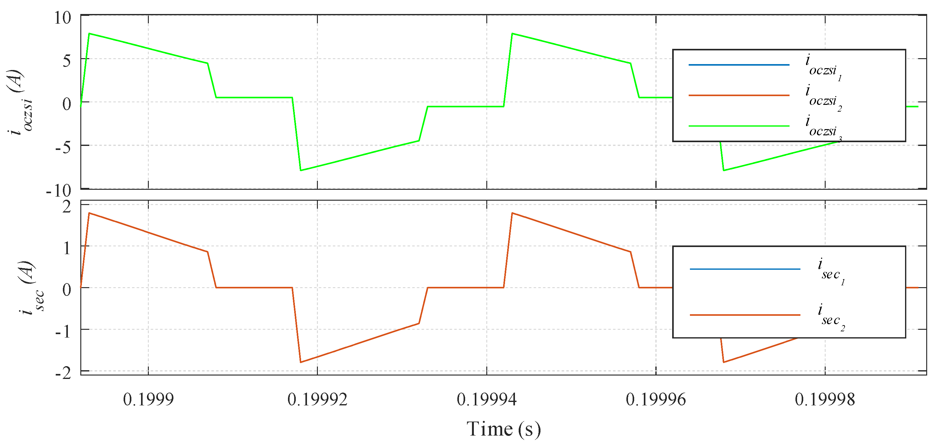
Since the study is in balanced power conditions, the same current
is expected on the three CZSI modules and RMS value can be estimated from Equations (
3) and (
6) to be around 5.6 A and 4.8 A respectively.
Figure 7 validates that under balanced conditions the current on primary modules are equal. It can be observed that during shoot-through times, there is a non-zero current on CZSI modules output and in conduction mode. On the other hand, the current on the secondary ports, does not present non-zero current in shoot-through times and thus the effect of parasitic elements on MF link are decoupled from primary side.
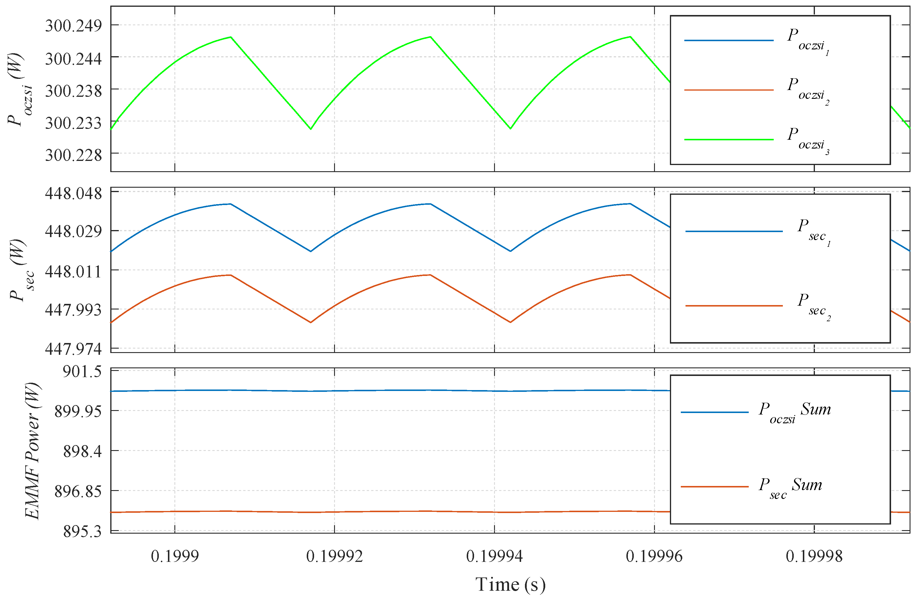
Figure 8 presents the average power on primary and secondary ports. First, the average output power on CZSI modules are shown in the first graphic and all of them are overlapped as expected for balanced conditions. In the same fashion, the average power in secondary side is balanced in both secondary outputs, and finally it can be observed that the sum of the average power of the three CZSI modules, matches with the sum of the average power on the secondary ports, and the difference between both is attributed to parasitic resistance in the MF link.
Once the operation under balanced conditions are validated, power imbalance studies were carried out. In order to appreciate the power imbalance, different irradiance were applied to each CZSI module: 900 W/m for module 1, 500 W/m in module 2, and 300 W/m to module 3. Variable loads were kept on each secondary output in order to obtain the maximum power extraction. Also a fixed 0.37 in all modules was set to put the system in MPP; since the higher is imposed to all coupled modules, a master-slave configuration is used, selecting the module with higher irradiance as the master.
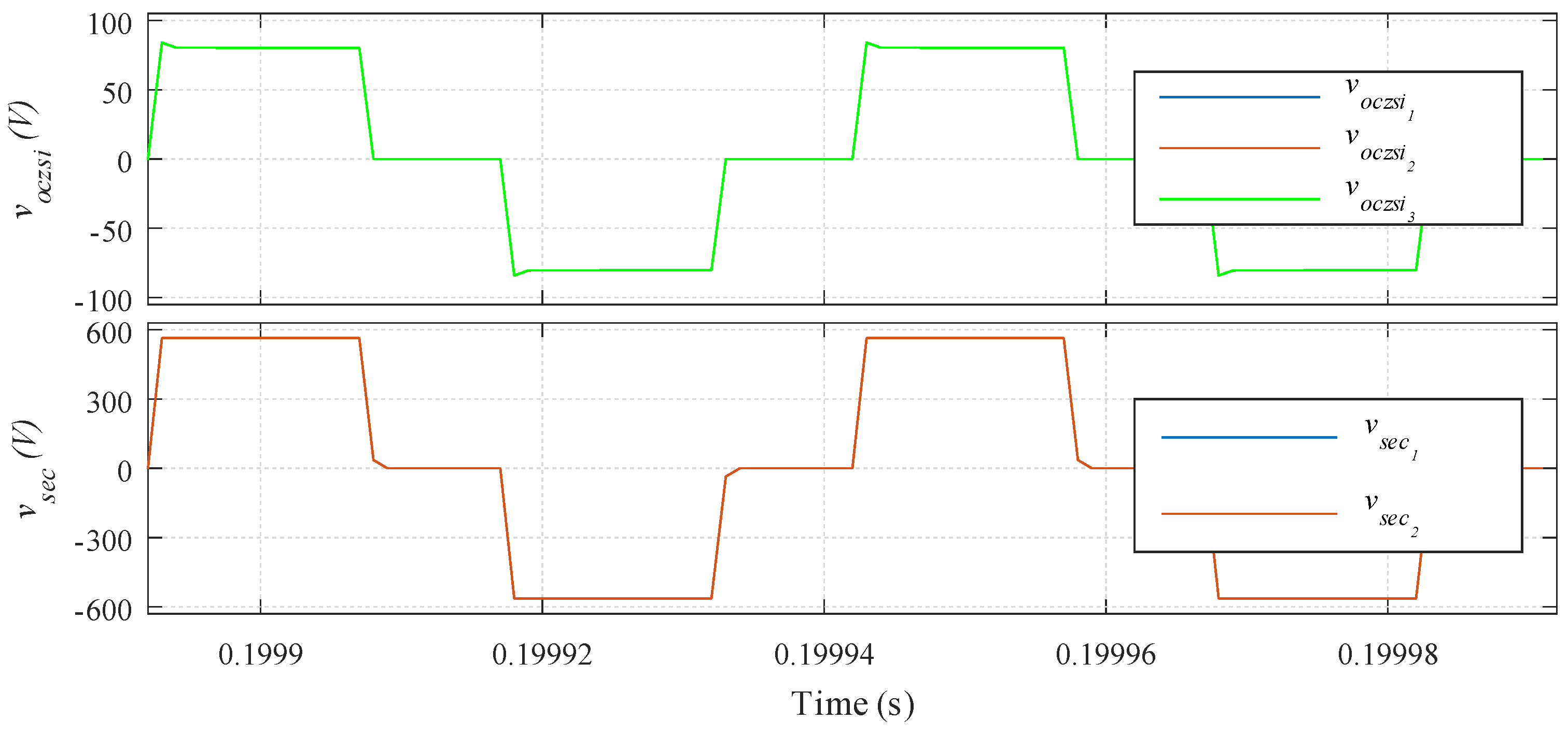
Voltages in primary and secondary ports in steady state are shown in
Figure 9. Voltage in primary ports are the output of CZSI modules and all three of them presents the same
value of 80 V during conduction state, and zero voltage in shoot-through states despite the imbalance applied. Similarly, the voltage on the secondary side has the same waveform with the gain of the MF link in the magnitude, passing from 80 V peak on primary side to 560 V peak on the secondary side. This validates that voltage balance is kept in primary and secondary ports despite power imbalance.
Figure 10 shows the steady state current on primary and secondary ports and it can be observed that currents
,
and
are different in function of the power supplied by the corresponding PV array. The non-zero current can be see during shoot-through state produced by parasitic elements in MF link. Considering, all primary ports have the same voltage, and each one has different current values, it validates that each port is managing different power levels. Despite the imbalance in CZSI modules, the second graphic shows that the current on secondary ports are equal without non-zero current during shoot-through states, which validates a balanced and decoupled power on secondary ports.
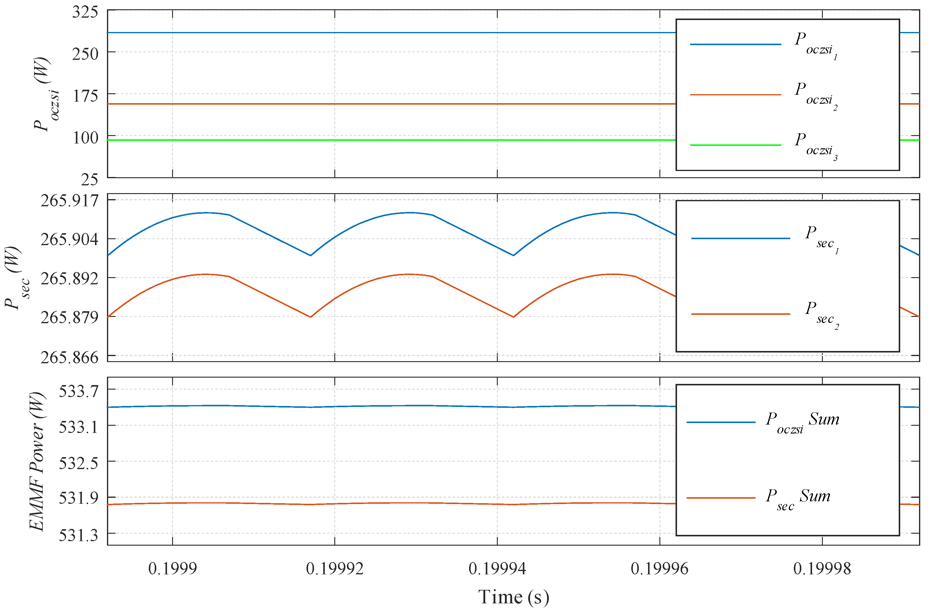
Figure 11 shows the power in primary ports as well as the average power in secondary ports. It can be see that each module has a different average power in primary side, in contrast to the secondary side that has exactly the same average power in both secondary ports.
When comparing the sum of the average power on primary and secondary side it is basically the same, but similar to balanced conditions, a small difference can be observed due to leakage inductance which produces the non-zero current present in primary side but not in secondary side. Finally a summary of the results obtained in the simulation studies is presented in
Table 2.
4.2. Experimental Results
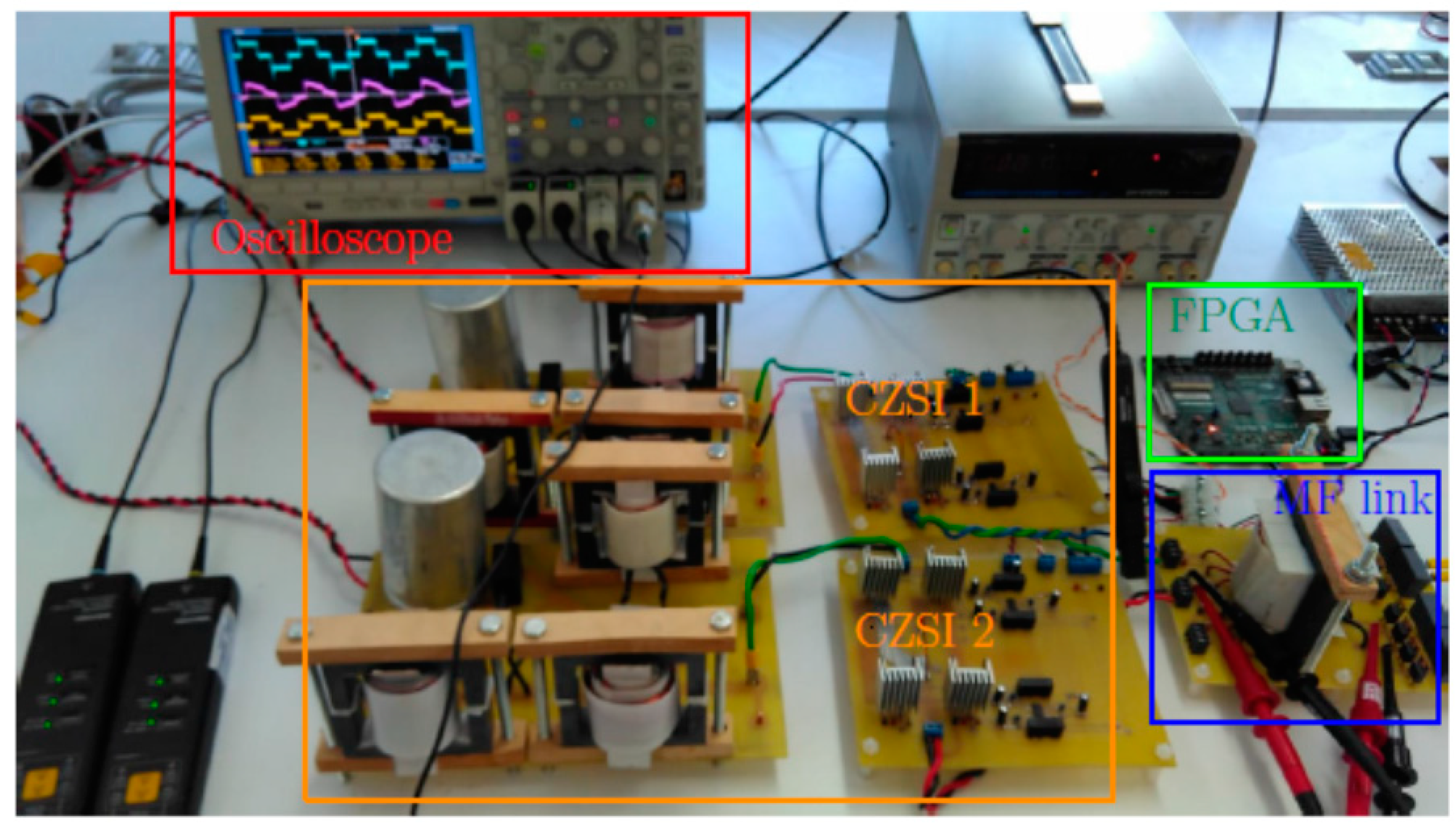
Once the CZSI modules and MF link were validated through simulations, an experimental prototype has been tested in multiport configuration. The prototype is shown in
Figure 12 and consists in 2 input CZSI modules, a magnetic link and two secondary cells with a diode full-wave rectifier on the output. The MF link consist on a multiport transformer with 15 turns on each primary port and 106 turns on each secondary port, built in a N27 E-80 ferrite core. Each CZSI module is energized by a PV panel array consisting on two 30 V, 8,33 A, 250 W panels connected in series achieving 60V at its MPP. Tests were carried out applying a 940
resistive load to the output in order to demand 470 W at MPP. The CZSI modules were operated with a fixed
as marked in
Table 1, but due to ambient conditions, only 60% of the array power was produced. Despite the last, tests validates the behavior of the system with a PV system supply.
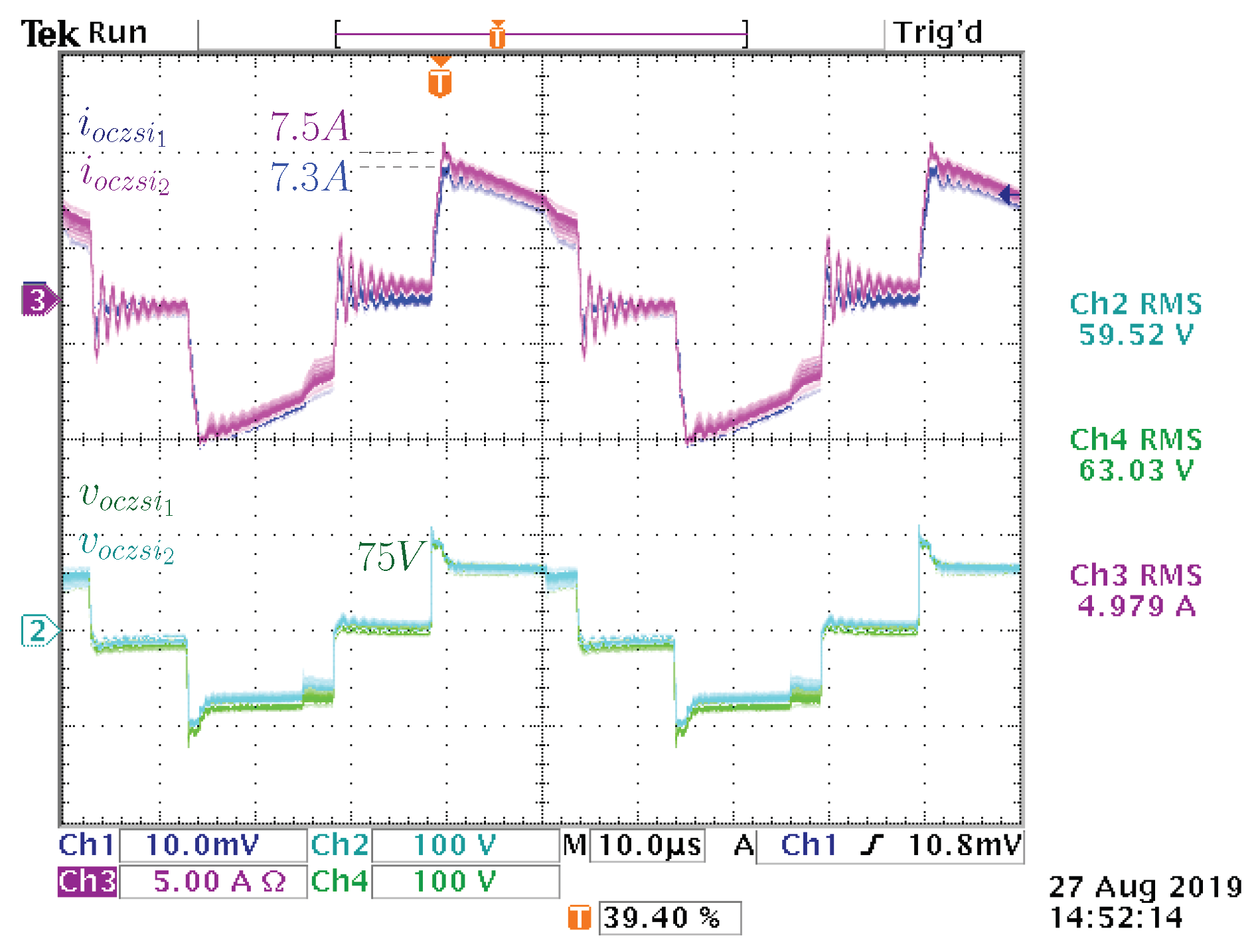
In
Figure 13 the performance of the prototype under balanced conditions is shown. The currents
and
are on channels 1 and 3 respectively, it can be see that they are overlapped with very small variations with a peak value of 7.5 A and 7.3 A on conduction mode, giving an approximate RMS value of 5 A; it can be noticed that the values are consistent with the simulation presented in
Figure 7 with a peak value around 7.5 A and descending to 4.5 A. A high-frequency component oscillation due to a resonance between the leakage inductance of the MF link and the parasitic capacitance of the MOSFET can be appreciated during shoot-through times. In channels 2 and 4, voltages
and
are shown and are also equal with a
near to 75 V for a more-less 60 V RMS on both modules. The
values obtained are similar to the ones presented in
Figure 6 and the behavior is consistent showing a small spike during conduction state. The similar values of both CZSI values confirm that both PV systems are in a balanced state. In balanced state, both modules extracted 300 W from each PV array for a 600 W output power.
Once the performance of the prototype was validated in balanced conditions, a test under power imbalance was performed using the same two PV panels arrays of the balanced test. The resistive load and duty cycle was also kept the same as before. Additionally, partial shade was applied to the PV panel array in module 2 in order to introduce the power imbalance.
In
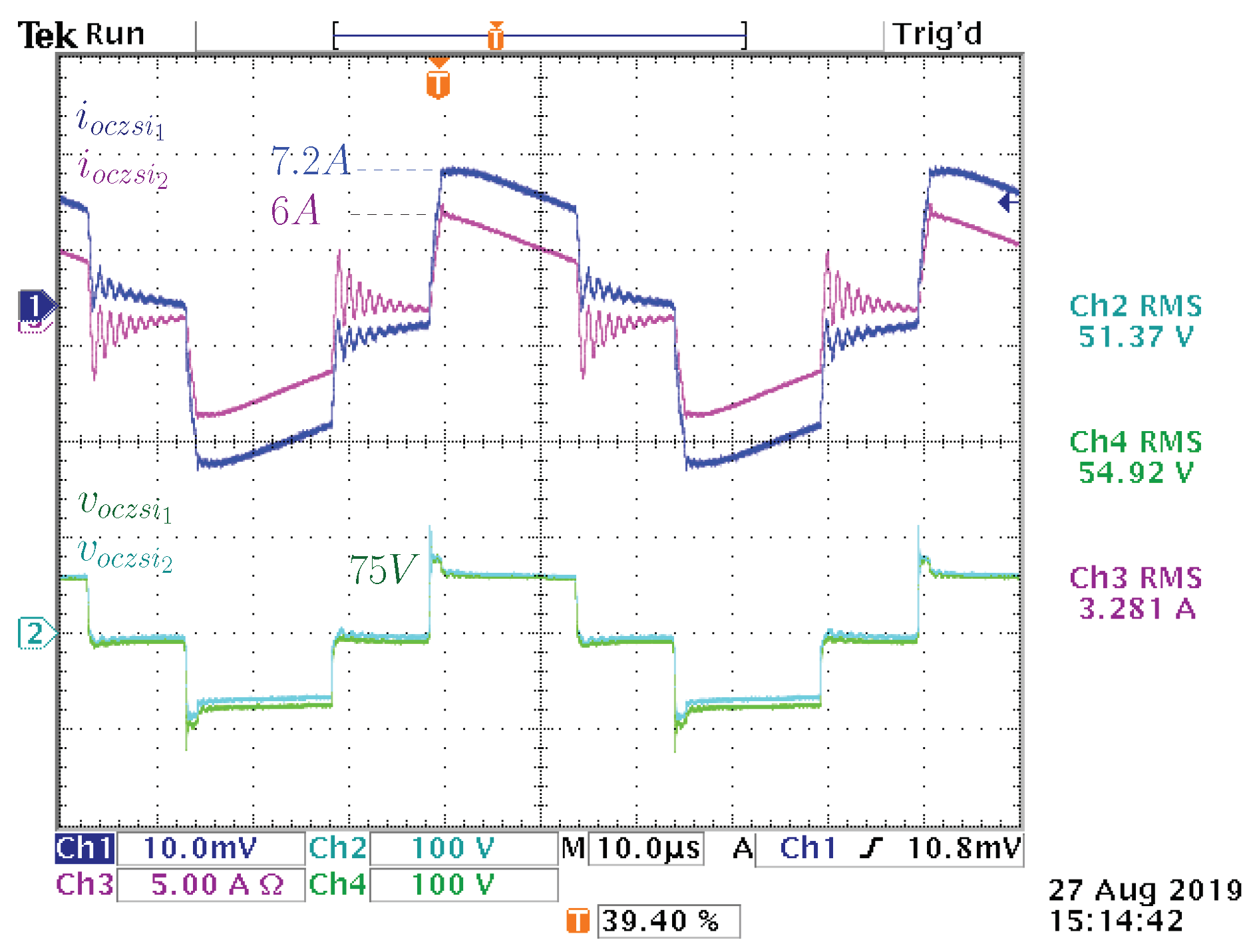
Figure 14, current
in module 1 and 2 can be observed on channel 1 and 3 respectively. It can be noted that the same high frequency oscillation due to resonance between MOSFET’s parasitic capacitance and the leakage inductance of the MF link in
Figure 13 is also present under unbalanced conditions. Different current levels can be clearly appreciated, with 7.2 A peak on
and 6 A peak on
. Despite both cells have different current levels,
stays on the same level as in balanced condition with 75 V
. A non-zero current in
during shoot-through times can be observed and is related to the parasitic elements of the transformer.
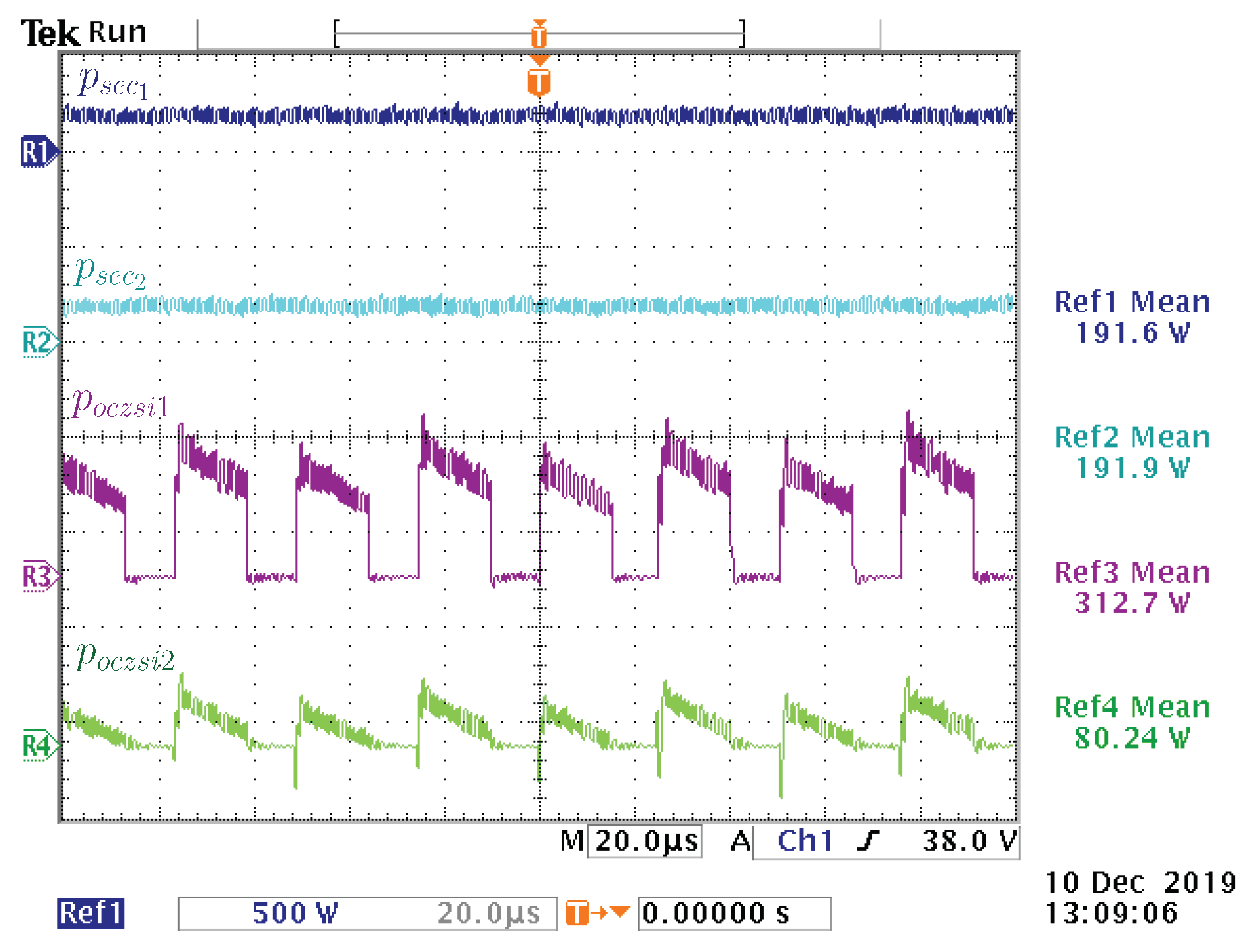
In
Figure 15 power in primary and secondary ports are presented. The first and second waveforms were taken after the diode full-wave rectifier and correspond to power in secondary ports 1 and 2 respectively; it can be see that they are equal in magnitude. The third and fourth waveform are the power in CZSI module 1 and 2 respectively, observe that they have different power levels and the sum matches the sum of power in the secondary side. The last validates that a balanced output can be generated despite power imbalances in the MF link inputs.
5. Discussion
From both simulation an experimental results, it was shown that current and voltage stress was kept in reasonable levels and only switches were affected by a voltage transitory. The last, is also present in boost-HB topologies, however over-current peaks are not present in CZSI as can be seen in
Figure 13 and
Figure 14, which suggest a lower current stress in semiconductor devices. In addition the shoot through operation gives more time to react to faults related to gate signals in switches: if the gate signals are lost due to external factor like irradiated noise from MF link or processor damage, the switches will be protected by the Z-source by limiting current until a protection flag is enabled. On the other hand, boost-HB topologies will just be damaged in case of losing gate signal, and thus suggesting that the CZSI enhance the reliability of the system.
For unbalanced power conditions, it can be seen that voltage between all PV arrays terminals remains similar for all the ports. However current supplied to each CZSI modules is different and is a function of the power supplied by the corresponding PV array. The voltage remains similar for all CZSI modules, as shown in simulation and experimental results. The current is the parameter that changes for the primary modules and thus the one that validates the transfer of different power levels in primary ports as shown in
Figure 10 and
Figure 13.
Despite the unbalanced power levels of the primary modules, the voltage is the same in secondary ports, but also the current is the same and thus the power on secondary side is balanced without additional actions, or modulation taken. The last is particularly useful for multilevel inverter applications where multiple isolated and balanced sources are required for proper operation. Topologies with galvanic isolation previously reported, usually implement multiple single-input single-output transformers in order to manipulate strings individually, this allows to follow MPP on each PV array and drive the transformer. However this produce different output on secondary side for each string and thus requires to be balanced by some added control strategy.


 ,
, 


