Article

A Compact Size Wideband RF-VGA Based on Second Generation Controlled Current Conveyors

by
J. del Pino
1,†,
Sunil L. Khemchandani
1,*,†,
D. Galante-Sempere
1,† and
C. Luján-Martínez
2,†
1
Departamento de Ingeniería Electrónica y Automática, Institute for Applied Microelectronics (IUMA), Universidad de Las Palmas de Gran Canaria, E-35017 Las Palmas de Gran Canaria, Spain
2
Departamento de Ingeniería Electrónica, Escuela Superior de Ingenieros, Universidad de Sevilla, E-41092 Las Palmas de Gran Canaria, Spain
*
Author to whom correspondence should be addressed.
These authors contributed equally to this work.
Electronics 2020, 9(10), 1600; https://doi.org/10.3390/electronics9101600
Submission received: 9 September 2020 / Revised: 28 September 2020 / Accepted: 29 September 2020 / Published: 30 September 2020
(This article belongs to the Special Issue CMOS Power Amplifier Design and Applications)

Abstract

:
This paper presents a methodology to design a wideband radio frequency variable gain amplifier (RF-VGA) in a low-cost SiGe BiCMOS 0.35 μ m process. The circuit uses two Class A amplifiers based on second-generation controlled current conveyors (CCCII). The main feature of this circuit is the wideband input match along with a reduced NF (5.5–9.6 dB) and, to the authors’ knowledge, the lowest die footprint reported (62 × 44 μ m2 area). The implementation of the RF-VGA based on CCCII allows a wideband input match without the need of passive elements. Due to the nature of the circuit, when the gain is increased, the power consumption is reduced. The architecture is suitable for designing wideband, low-power, and low-noise amplifiers. The proposed design achieves a tunable gain of 6.7–18 dB and a power consumption of 1.7 mA with a ±1.5 V DC supply. At maximum gain, the proposed RF-VGA covers from DC up to 1 GHz and can find application in software design radios (SDRs), the low frequency medical implant communication system (MICS) or industrial, scientific, and medical (ISM) bands.

1. Introduction

In radio frequency integrated circuits, the design of wideband amplifiers has been intensively discussed over the past few decades [1]. The most widely used wideband amplifier architecture is the distributed amplifier, which requires high power consumption and a large area due to the considerable number of stages and the extensive use of inductors [2,3,4].
Another commonly used technique is the use of feedback amplifiers [5,6,7,8,9,10]. This solution offers a good return loss, but, due to the feedback, it is difficult to achieve a low noise figure with a reasonable power consumption.
As an alternative to these two previous topologies, some authors have proposed the design of wideband circuits by converting narrowband circuits into broadband [11,12,13]. This is usually achieved by modifying the input matching network to act as a broadband filter and replacing the narrowband load (typically a tank circuit) with any of the wideband RC load implementations: series-peaking, shunt-peaking, shunt-series-peaking, etc. [14,15,16]. Again, as in the case of the distribute amplifier technique, the main limitation of this solution is the area as they use a large number of inductors. Note that the issues of large area and high power consumption are aggravated when variable gain is desired.
To reduce the area constraints, some authors have proposed the use of common-base or common-gate wideband amplifiers [14,15,16]. These topologies take advantage of the fact that, in such configurations, it is possible to obtain a broadband input impedance equal to 50 Ω by properly biasing the transistor. However, the gain and noise figure are determined by this biasing and consequently fixed to a certain value.
At system level, when implementing a wideband analog RF front-end, the most popular scheme includes a wideband low noise amplifier (LNA) followed by a variable gain amplifier (VGA). This maximizes the dynamic range of the upcoming stages and prevents the saturation of the receiver if a high-powered signal is received [17]. In these cases, the implementation of a wideband RF-VGA is of upmost interest.
This work addresses the design of a very compact, low power, low voltage, and high bandwidth RF-VGA using second generation controlled current conveyors. A CCCII is a four terminal device that can perform many useful analog signal processing functions when arranged with other electronic elements in specific circuit configurations [18]. CCCIIs have been successfully used in high frequency current mode applications such as filters [19] and LNAs [20]. The proposed radio frequency variable gain amplifier (RF-VGA) is based in the CCCII proposed in [21] and has been designed and fabricated in a low cost 0.35 μ m SiGe BiCMOS technology. The rest of the paper goes as follows: Section 2 reviews the CCCII and describes the proposed RF-VGA topology and the design methodology, Section 3 focuses on the circuit performance and the analysis of the obtained results; finally, some conclusions are drawn in Section 4.

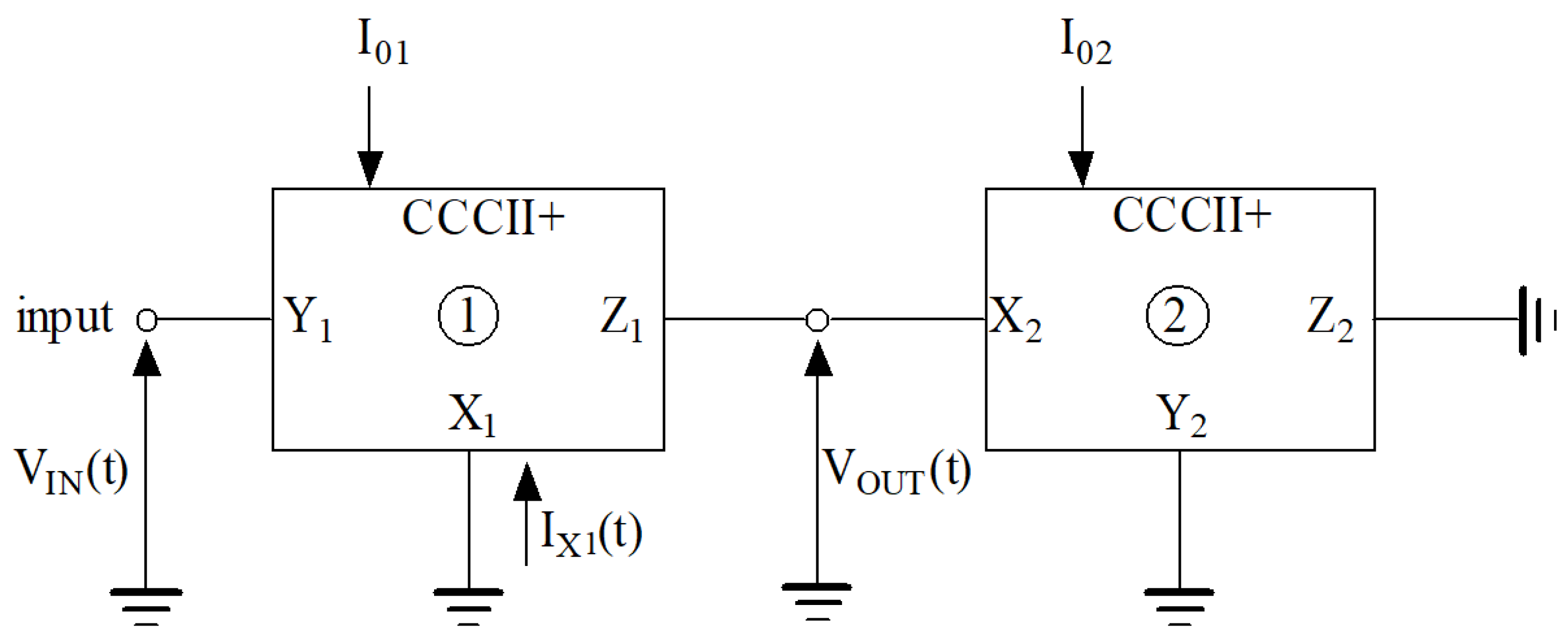
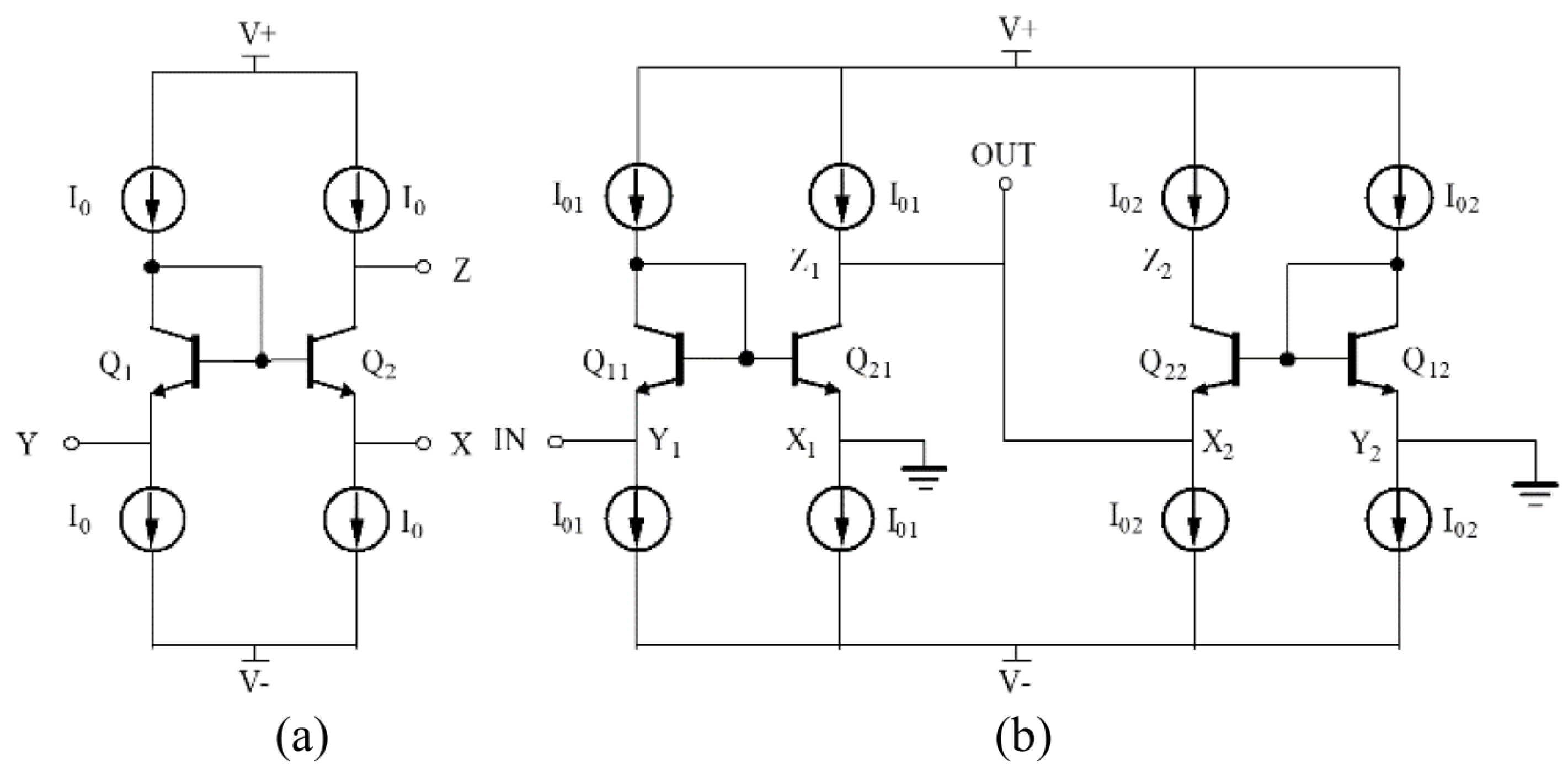
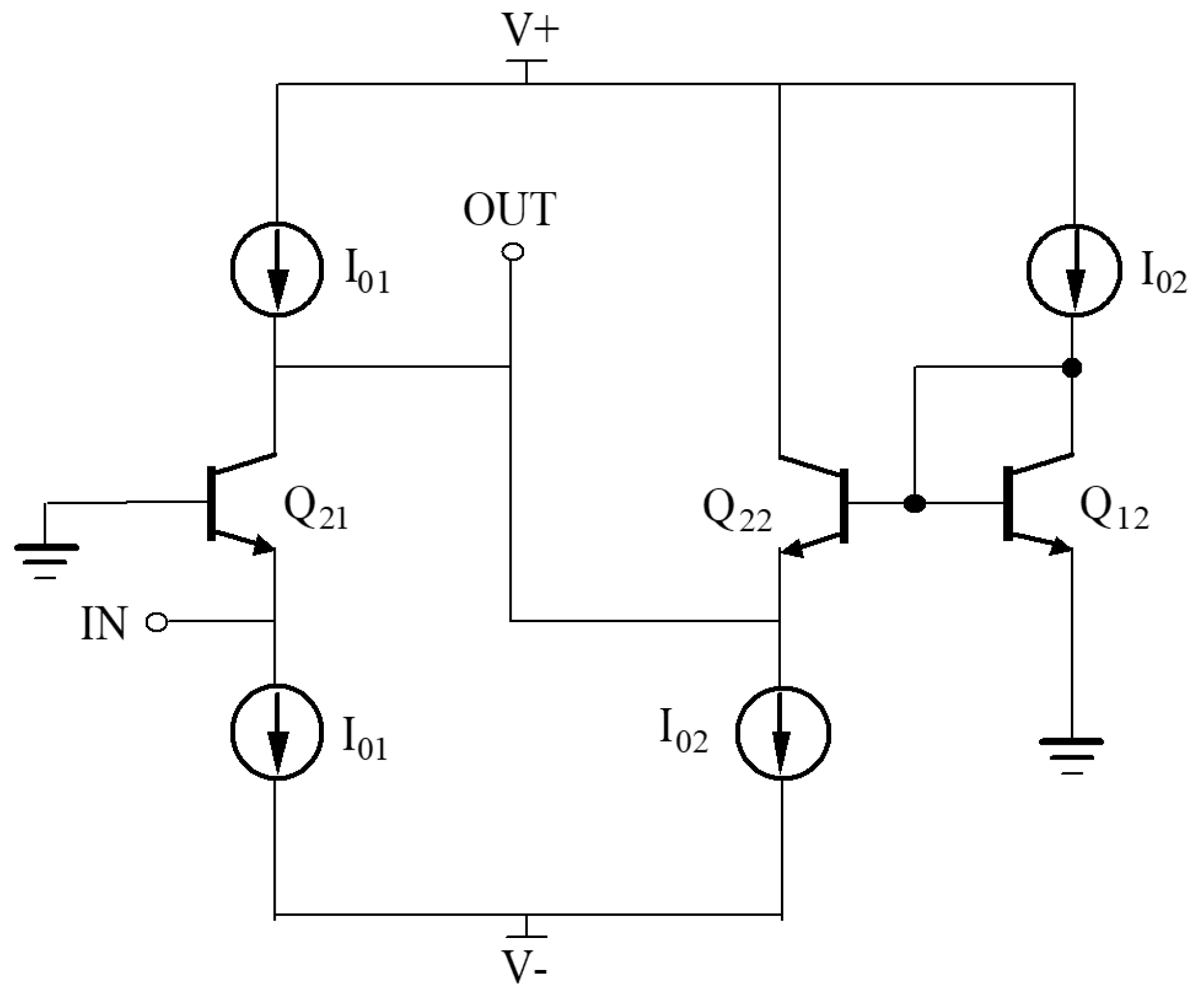
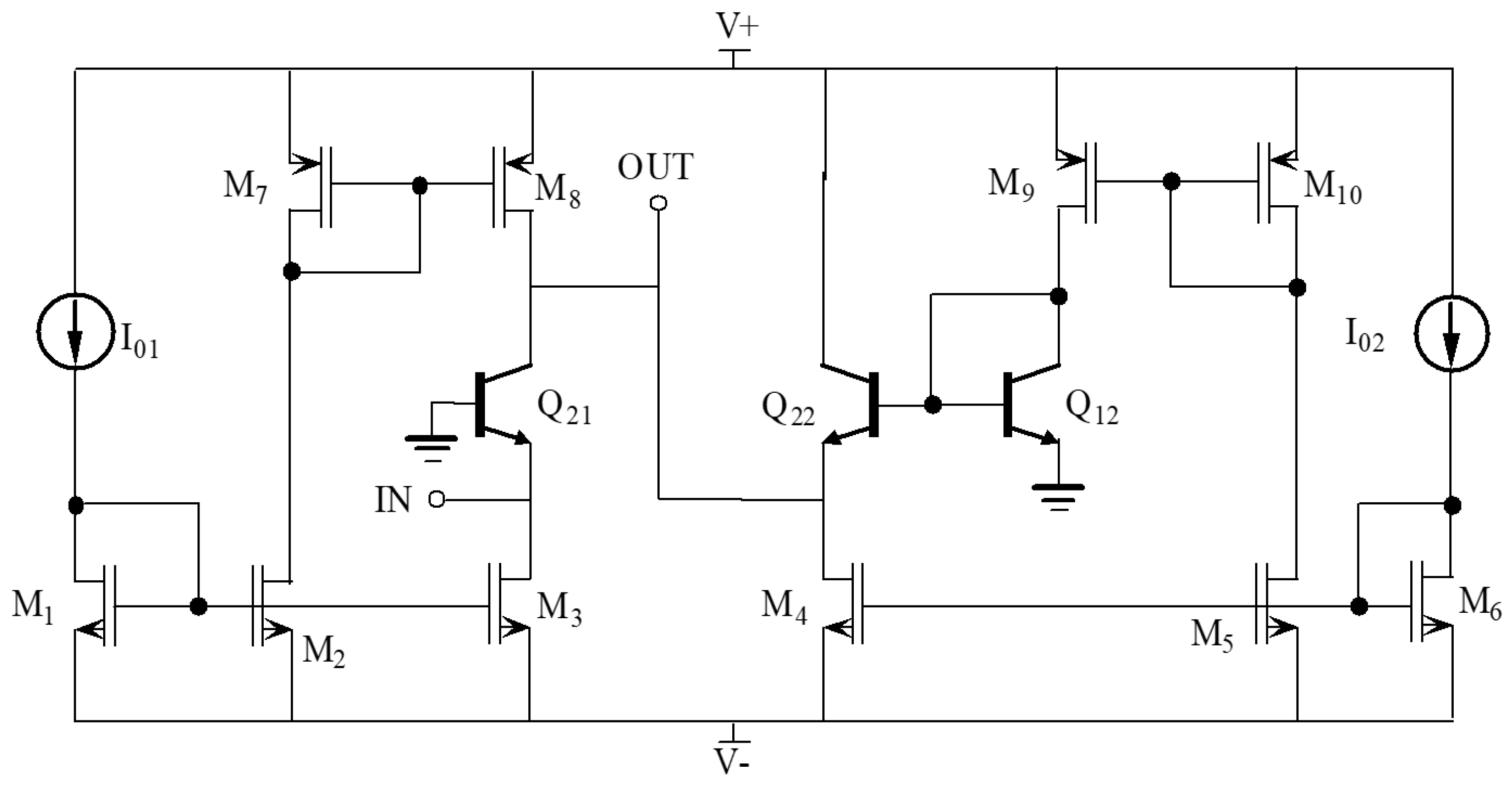
2. RF-VGA Based on the Current Conveyor

CCCIIs can be used to implement numerous functions, such as filtering, amplification, or impedance transformation. They also provide better performance than traditional OTAs, namely, improved power consumption and larger cut-off frequency [19].
A CCCII is a device with three ports (X, Y and Z) and a DC bias current ( I 0 ). Each port is characterized by an impedance ( Z X , Z Y and Z Z ) resulting from the implementation of the conveyor with non-ideal components. These impedances are defined by parasitic elements, which are highly dependent on the selected technology of fabrication and the bias current I 0 . Thus, the concept of controlled current conveyor appears due to this dependence on I 0 . The relationship that governs the interactions between the ports of the conveyor is defined as follows:
  • between ports X and Z the device acts as a current follower,
  • between ports Y and X it operates as a voltage follower,
  • between ports Z and Y it behaves as a transconductor.
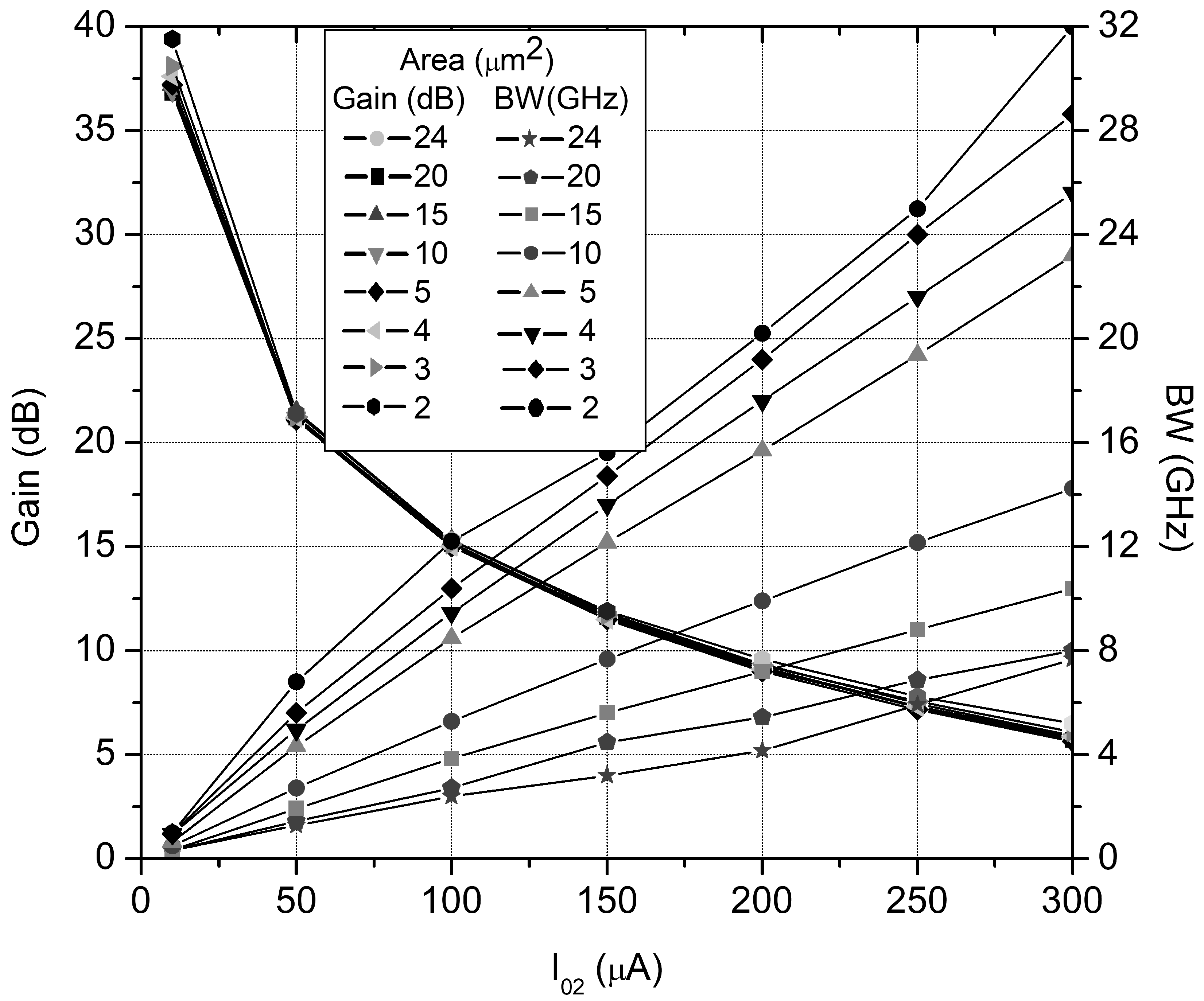
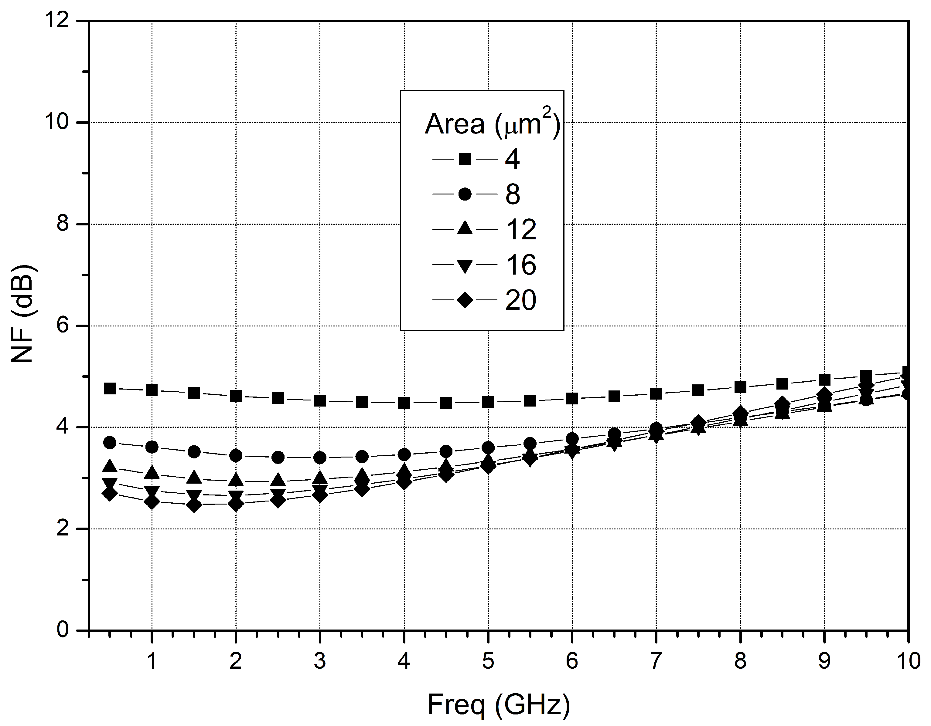
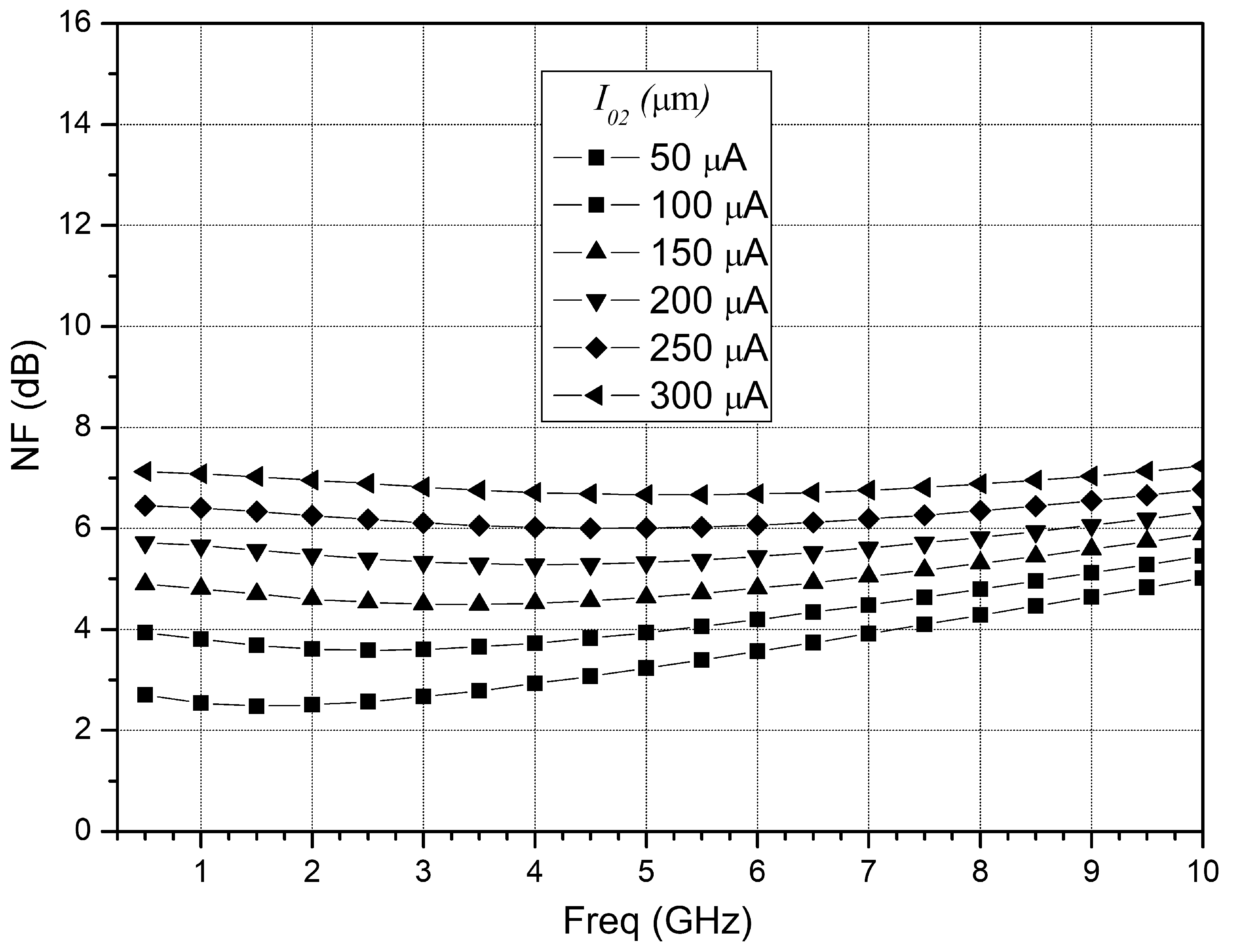
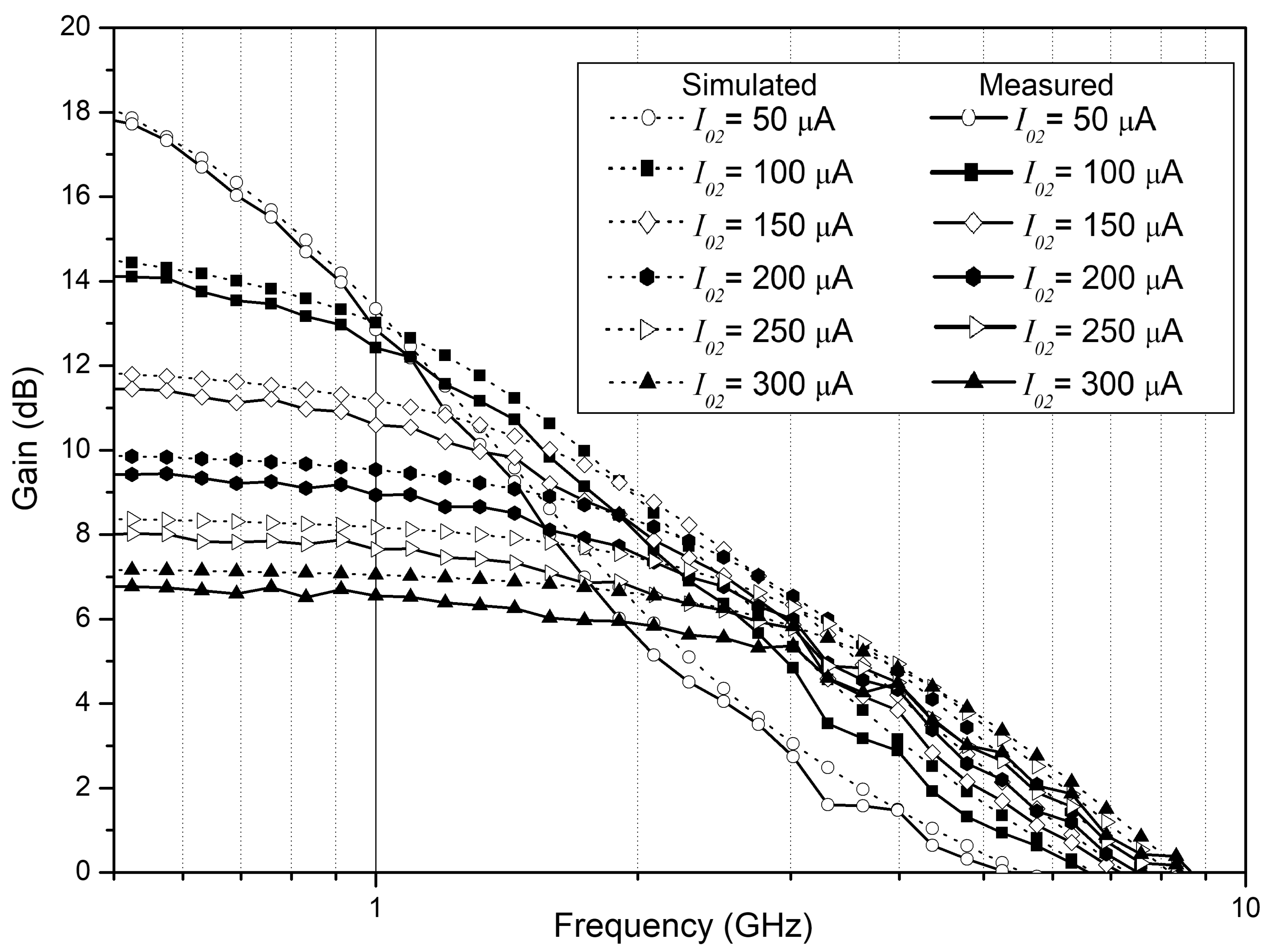
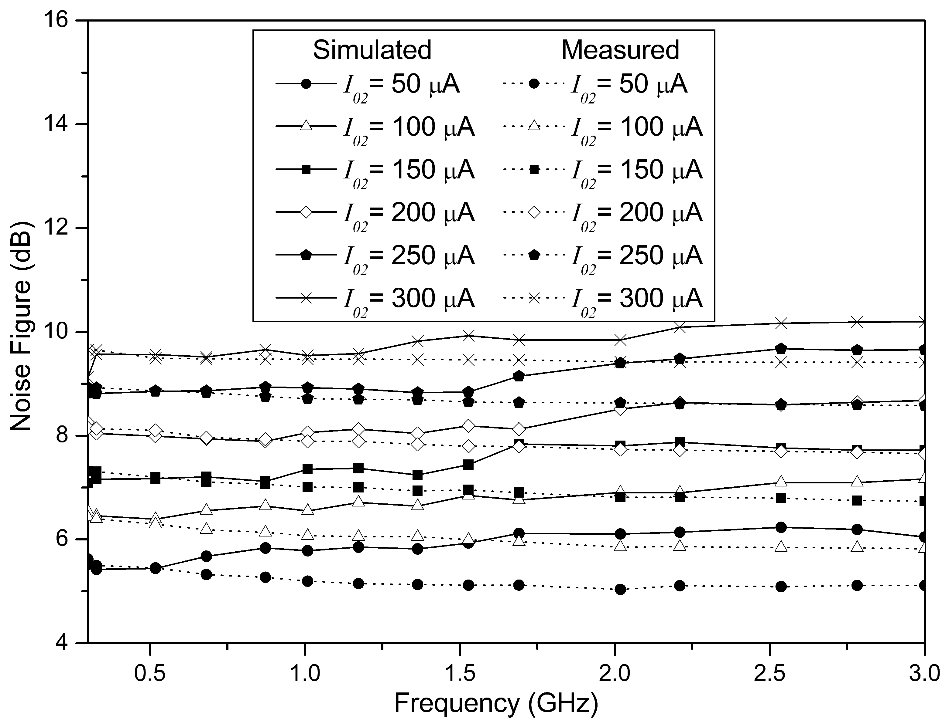
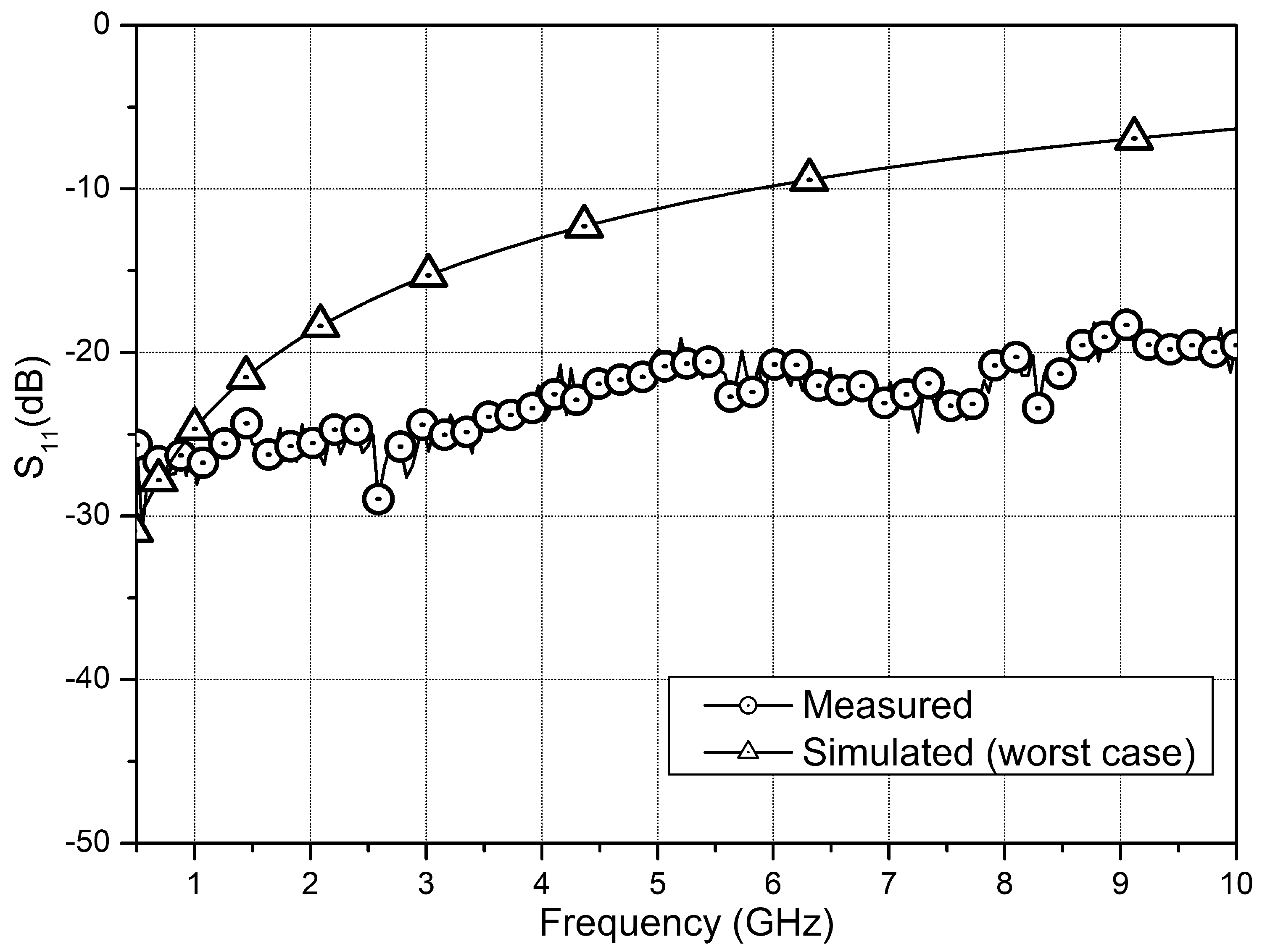
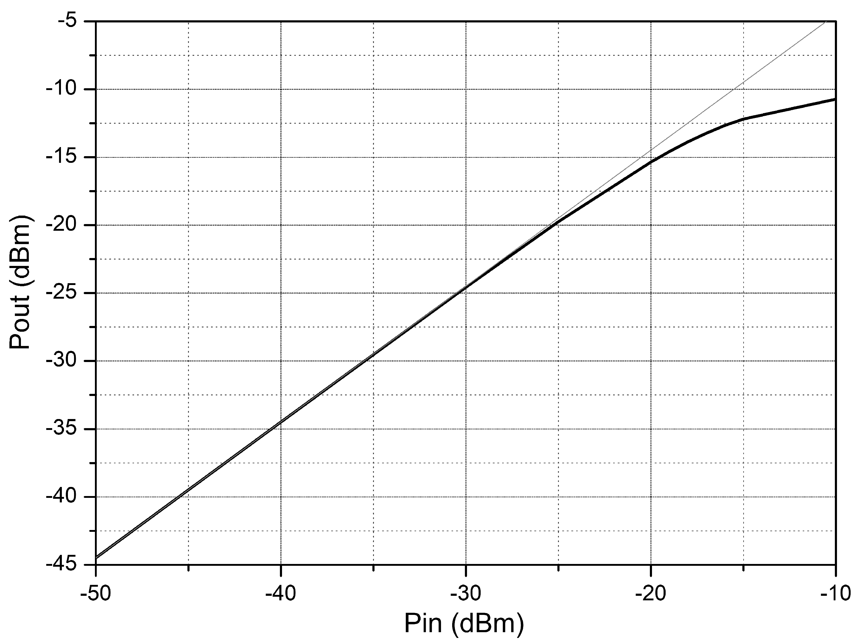
The matrix that defines these relationships is given by
I Y V X I Z = Y Y ( I 0 ) 0 0 β ( s ) Z X ( I 0 ) 0 0 α ( s ) Y Z ( I 0 ) · V Y I X V Z
where Y Y is the conductance of port Y, and Y Z , the conductance of port Z. In addition, the terms α ( s ) and β ( s ) represent the unity current and voltage transfer functions. The resistive component of Z X (defined as R X ) is particularly relevant since it can be used to define the interaction between ports.
Variable gain amplifiers can be implemented using CCCIIs [19,20,21], where the gain tuning is performed by means of adjusting the bias current of the conveyor. The dependence of R X on the bias current I 0 can be exploited to provide wideband input matching without including a single passive component, resulting in a circuit with a very low input return loss. This situation is desirable in scenarios where the amplifier is the first integrated circuit in the reception path. For example, if a preceding LNA is added externally, the proposed RF-VGA facilitates impedance matching with this element, and the signal coming from the LNA is received with a very low loss. In addition, the proposed design can potentially obtain a high cut-off frequency and low die footprint due to the reduced number of active devices needed to implement the conveyor.
To implement an RF-VGA, two CCCII blocks are connected as shown in Figure 1 [20]. Provided that the impedances Z X 1 and Z X 2 are entirely resistive, V I N ( t ) is transformed into a current I I N ( t ) . This current is then converted into a voltage signal again thanks to Z X 2 . Due to the relationship between R X and the bias current I 0 , it can be proved that the gain G of the amplifier reduces to:
G = V O U T ( t ) V I N ( t ) = I 01 I 02
Since the node Y 1 presents a high input impedance [19], the input signal is applied at node X 1 . By doing so, the input impedance is reduced and can be controlled by the bias current I 01 . Thus, the input impedance Z I N of the RF-VGA can be adjusted by means of adjusting the value of the bias current I 01 , which is fixed to obtain | Z I N | = 50 Ω .
The value of the bias current I 01 can be fixed to perform wideband input matching, and so the gain can be adjusted by setting the value of I 02 . Due to the inversely proportional relationship given by (2), it is possible to increase the gain by reducing the bias current I 02 . Therefore, higher gain settings lead to lower power consumption. A simple Class-A implementation scheme with CCCIIs is shown in Figure 2a. To obtain the structure depicted in Figure 1, nodes Z 1 and X 2 must be connected together, yielding the circuit depicted in Figure 2b. As mentioned above, the input signal is applied at node X 1 to facilitate input matching, allowing the elimination of transistor Q 11 . The resulting scheme after simplification is presented in Figure 3. With this result, the number of BJTs is reduced as much as possible, yielding a higher cut-off frequency and a better noise performance [22]. The required values of the bias current I 01 obtained in simulation to achieve a 50 Ω input impedance are plotted in Figure 4 for various transistor areas from the 0.35 μ m SiGe design kit used.
The voltage gain and the bandwidth of the RF-VGA are plotted in Figure 5. The values between 100 μ A and 250 μ A present a trade-off between gain and bandwidth and can be used to determine the optimal combination of device area and bias current I 02 . When I 02 augments, the gain of the circuit drops while the bandwidth raises. The gain is not significantly affected by the variation in the transistor area, but, as expected, the bandwidth is increased if the area is reduced. Although the RF-VGA may be preceded by an LNA, its noise figure (NF) is one of the most relevant parameters in the design. If the LNA gain is low, the RF-VGA must provide a reduced NF and high gain to avoid degradation of the receiver performance.
Depending on the application of interest, a trade-off between gain, noise, and bandwidth must be considered by the designer. In this implementation, the number of elements in the signal path is kept as low as possible (only tree BJTs), and there is a total absence of passive elements. Consequently, the noise introduced by spurious elements is minimized and the main noise contribution is due to the input transistor Q 21 . Figure 6 depicts the simulated NF of the circuit for different transistor areas, where it is shown that the NF decreases when the device area is increased. The noise figure of the RF-VGA is also plotted against I 02 in Figure 7 for a transistor area of 20 μ m2. Note that the noise figure is strongly dependent on the bias current, so that, when I 02 increases, the gain is reduced and the NF augments. If a high gain and a low NF is desired, a lower I 02 and a higher transistor area are required. However, this situation limits the achievable bandwidth since a low bias current combined with a high aspect ratio yields a reduced frequency performance (see Figure 5). As a result, a trade-off between noise figure, gain, and bandwidth is present and should be considered depending on the design specifications.
The final RF-VGA schematic is shown in Figure 8, where the current sources have been replaced with MOS transistors. The RF-VGA was designed and laid out in a BiCMOS SiGe 0.35 μ m process with a DC supply of ±1.5 V. The layout of the circuit is presented in Figure 9. The layout was realized taking into account critical aspects of analog RFICs, such as circuit symmetry and transistor matching techniques to reduce PVT variations. The selected areas for each transistor were chosen to achieve a maximum gain of 18 dB and a 900 MHz bandwidth with a total current consumption below 2 mA. The size of Q 21 is 20 μ m2, which is twice the size of Q 12 and Q 22 , with 10 μ m2 each. The aspect ratio of the NMOS and PMOS transistors is 20/1 ( μ m/ μ m).

3. Measurements

Probe pads were added for on–wafer measurements. Two ground-signal-ground (GSG) and two signal-ground-signal (SGS) pads structures with 150 μ m pitch were used. The DC supply is ±1.5 V and the amplifier draws a current of 1.7 mA. The total chip size of the RF-VGA including pads is 800 × 430 μ m2, but the core of the circuit occupies an area as low as 62 × 44 μ m2. The voltage gain of the RF-VGA is plotted in Figure 10 for a frequency range of DC–3 GHz vs. bias current I 02 . A good agreement between measurement and simulation can be found with an error below ±1.1 dB in the entire band. As expected, when I 02 is increased, the gain of the circuit decreases while the bandwidth raises. The simulation and measurement results of the NF of the proposed design are depicted in Figure 11. As can be seen, the NF increases with the bias current I 02 . A reduced bias current (i.e., higher gain) is needed if a low noise figure is required. As mentioned above, the drawback is a reduction in the bandwidth of the amplifier. In many applications, it is desirable to extend the bandwidth thus a multistage approach or a bandwidth enhancement technique would be needed to obtain a high-gain and wide-band. For NF, the error between simulation and measurement is below 1.4 dB.
Another key parameter for the performance of the RF-VGA is the input return loss. When the LNA is implemented externally, the RF-VGA is the first integrated device in the receiver; thus, a broadband 50 Ω input match is required. The simulated and measured S 11 are shown in Figure 12, where the measured magnitude for the S 11 is better than 20 dB for frequencies up to 10 GHz.
The linearity of the proposed RF-VGA was evaluated by measuring the input 1-dB compression point ( P 1 d B ) using a test tone of 666 MHz. The measurement results for maximum gain settings ( I 01 = 600 μ A and I 02 = 50 μ A) are plotted in Figure 13, obtaining a value of –20.18 dBm for the input P 1 d B .
A summary of the performance of the proposed RF-VGA versus I 02 is presented in Table 1 for I 01 = 550 μ A and V D C = ± 1.5 V. A brief overview of similar works available in the literature is given in Table 2 [23,24,25,26,27,28,29,30]. With the exception of [26], which uses 40 nm technology, our work has better bandwidth. Compared with other authors, a good trade-off between gain and bandwidth is obtained. We have achieved a competitive noise figure, not exceeding 9.6 dB for the worst case. The power consumption is small, but not the lowest one, this is because the others authors have used more advanced technologies. To the best of the authors’ knowledge, the present work achieves the lowest area occupation reported in the literature while showing competitive performances in terms of gain, NF and BW with a power consumption similar to that of other proposed solutions.

4. Conclusions

A very compact, low power, low voltage and high bandwidth RF-VGA based on the cascade connection of two CCCII blocks has been presented. The circuit was implemented in a standard low cost SiGe BiCMOS 0.35 μ m process. A gain control from 6.7 to 18 dB is obtained varying the bias current of the circuit. The present work achieves, to the authors’ knowledge, the lowest area occupation. For a polarization current I 02 of 50 μ A, the circuit achieves a power consumption of 1.7 mA with a ±1.5 V DC supply, an input return loss better than 20 dB from DC up to 10 GHz and a noise figure from 5.5 dB at maximum gain settings to 9.6 dB at minimum gain settings. Finally, the measured P 1 dB is −20.18 dBm. The RF-VGA achieves a very competitive trade-off between gain, noise figure, input return loss, power consumption, and die footprint, making this architecture suitable for the design of compact wide-band, low-power, and low-noise variable gain amplifiers.

Author Contributions

J.d.P., S.L.K., D.G.-S. and C.L.-M., these authors contributed equally to this work. All authors have read and agreed to the published version of the manuscript.

Funding

This work was funded in part by the Spanish Ministry of Science, Innovation and Universities (RTI2018-099189-B-C22) and by the Canary Agency for Research, Innovation and Information Society (ACIISI) of the Canary Islands Government by ProID2017010067 and TESIS2019010100 grants.

Conflicts of Interest

The authors declare no conflict of interest.

Abbreviations

The following abbreviations are used in this manuscript:
BWbandwidth
CCIIsecond-generation current conveyor
CCCIIsecond-generation controlled current conveyor
ISMindustrial, scientific and medical
LNAlow noise amplifier
MICSmedical implant communication system
RF-VGAradio frequency variable gain amplifier
SDRsoftware design radio
VGAvariable gain amplifier

References

  1. Díaz, R.; Khemchandani, S.L.; Vázquez, H.; Suárez, F. Design Of Low-Noise Amplifiers for Ultra-Wideband Communications, 1st ed.; McGraw-Hill Professional: New York, NY, USA, 2014; ISBN 978-007-182-312-8. [Google Scholar]
  2. Ballweber, B.M.; Gupta, R.; Allstot, D.J. A fully integrated 0.5–5.5 GHz CMOS distributed amplifier. IEEE J. Solid-State Circuits 2000, 35, 231–239. [Google Scholar] [CrossRef]
  3. Guan, X.; Nguyen, C. Low-power-consumption and high-gain CMOS distributed amplifiers using cascade of inductively coupled common-source gain cells for UWB systems. IEEE Trans. Microw. Theory Tech. 2006, 54, 3278–3283. [Google Scholar] [CrossRef]
  4. Pino, J.D.; Khemchandani, S.L.; Mateos-Angulo, S.; Mayor-Duarte, D.; San-Miguel-Montesdeoca, M. Area Efficient Dual-Fed CMOS Distributed Power Amplifier. Electronics 2018, 7, 139. [Google Scholar] [CrossRef] [Green Version]
  5. Feng, C.; Yu, X.P.; Lu, Z.H.; Lim, W.M.; Sui, W.Q. 3–10 GHz self-biased resistive-feedback lna with inductive source degeneration. Electron. Lett. 2013, 49, 387–388. [Google Scholar] [CrossRef]
  6. Lee, J.; Cressler, J.D. A 3–10 GHz SiGe resistive feedback low noise amplifier for UWB applications. In Proceedings of the 2005 IEEE Radio Frequency Integrated Circuits (RFIC) Symposium-Digest of Papers, Long Beach, CA, USA, 12–14 June 2005; pp. 545–548. [Google Scholar] [CrossRef]
  7. Kim, C.-W.; Kang, M.-S.; Anh, P.T.; Kim, H.-T.; Lee, S.-G. An ultra-wideband CMOS low noise amplifier for 3–5-GHz UWB system. IEEE J. Solid-State Circuits 2005, 40, 544–547. [Google Scholar] [CrossRef]
  8. Vázquez, H.G.; Khemchandani, S.L.; Pulido, R.; Goñi-Iturri, A.; del Pino, J. A wideband active feedback LNA with a modified 3D inductor. Microw. Opt. Technol. Lett. 2010, 52, 1561–1567. [Google Scholar] [CrossRef]
  9. Sahafi, A.; Sobhi, J.; Koozehkanani, Z.D. Linearity improvement of gm-boosted common gate LNA: Analysis to design. Microelectron. J. 2016, 56, 156–162. [Google Scholar] [CrossRef]
  10. Jafarnejad, R.; Jannesari, A.; Nabavi, A.; Sahafi, A. A low power low noise amplifier employing negative feedback and current reuse techniques. Microelectron. J. 2016, 49, 49–56. [Google Scholar] [CrossRef]
  11. Ismail, A.; Abidi, A.A. A 3–10-GHz low-noise amplifier with wideband LC-ladder matching network. IEEE J. Solid-State Circuits 2004, 39, 2269–2277. [Google Scholar] [CrossRef]
  12. Bevilacqua, A.; Niknejad, A.M. An ultrawideband CMOS low-noise amplifier for 3.1–10.6-GHz wireless receivers. IEEE J. Solid-State Circuits 2004, 39, 2259–2268. [Google Scholar] [CrossRef]
  13. Chen, Z.; Gao, H.; Leenaerts, D.M.W.; Milosevic, D.; Baltus, P.G.M. A 16–43 GHz low-noise amplifer with 2.5–4.0 dB noise figure. In Proceedings of the IEEE Asian Solid-State Circuits Conference (A-SSCC), Toyama, Japan, 7–9 November 2016; pp. 349–352. [Google Scholar] [CrossRef] [Green Version]
  14. Shekhar, S.; Walling, J.S.; Allstot, D.J. Bandwidth Extension Techniques for CMOS Amplifiers. IEEE J. Solid-State Circuits 2006, 41, 2424–2439. [Google Scholar] [CrossRef]
  15. Li, Z.; Wang, C.; Li, Q.; Wang, Z. 60 GHz low-power LNA with high gm × Rout transconductor stages in 65 nm CMOS. Electron. Lett. 2017, 53, 279–281. [Google Scholar] [CrossRef]
  16. Pi, D.; Chun, B.; Heydari, P. A Synthesis-based Bandwidth Enhancing Technique for CML Buffers/Amplifiers. In Proceedings of the 2007 IEEE Custom Integrated Circuits Conference, San Jose, CA, USA, 16–19 September 2007; pp. 467–470. [Google Scholar] [CrossRef]
  17. Abidi, A.A. The path to the software-defined radio receiver. IEEE J. Solid-State Circuits 2007, 42, 954–966. [Google Scholar] [CrossRef]
  18. Sedra, A.; Smith, K. A second-generation current conveyor and its application. IEEE Trans. Circuit Theory 1970, 17, 132–134. [Google Scholar] [CrossRef]
  19. Fabre, A.; Saaid, O.; Wiest, F.; Boucheron, C. High frequency applications based on a new current controlled conveyor. IEEE Trans. Circuits Syst. I. Fundam. Theory Appl. 1996, 43, 82–91. [Google Scholar] [CrossRef]
  20. Seguin, F.; Godara, B.; Alicalapa, F.; Fabre, A. A gain-controllable wide-band low-noise amplifier in low-cost 0.8 μm Si BiCMOS yechnology. IEEE Trans. Microw. Theory Tech. 2004, 52, 154–160. [Google Scholar] [CrossRef]
  21. Seguin, F.; Fabre, A. 2 GHz controlled current conveyor in standard 0.8 μm BiCMOS technology. Electron. Lett. 2001, 37, 329–330. [Google Scholar] [CrossRef]
  22. Lee, S.; Choi, I.; Kim, H.; Kim, B. A Sub-mW Fully Integrated Wide-Band Receiver for Wireless Sensor Network. IEEE Microw. Wirel. Compon. Lett. 2015, 25, 319–321. [Google Scholar] [CrossRef]
  23. Wang, Y.; Afshar, B.; Ye, L.; Gaudet, V.C.; Niknejad, A.M. Design of a low power, inductorless wideband variable-gain amplifier for high-speed receiver systems. IEEE Trans Circuits Syst. I Regul. Pap. 2011, 59, 696–707. [Google Scholar] [CrossRef]
  24. Park, H.; Lee, S.; Lee, J.; Nam, S. A 0.1–1 Ghz CMOS variable gain amplifier using wideband negative capacitance. IEICE Trans. Electron. 2009, 92, 1311–1314. [Google Scholar] [CrossRef]
  25. Liu, H.; Boon, C.C.; He, X.; Zhu, X.; Yi, X.; Kong, L.; Heimlich, M.C. A wideband analog-controlled variable-gain amplifier with db-linear characteristic for high-frequency applications. IEEE Trans. Microw. Theory Tech. 2019, 64, 533–540. [Google Scholar] [CrossRef]
  26. Elkholy, M.; Shakib, S.; Dunworth, J.; Aparin, V.; Entesari, K. A wideband variable gain LNA with high OIP3 for 5G using 40-nm bulk CMOS. IEEE Microw. Wirel. Compon. Lett. 2017, 28, 64–66. [Google Scholar] [CrossRef]
  27. Baumgratz, F.D.; Saavedra, C.; Steyaert, M.; Tavernier, F.; Bampi, S. A wideband low-noise variable-gain amplifier with a 3.4 dB NF and up to 45 dB gain tuning range in 130-nm CMOS. IEEE Trans. Circuits Syst. II Exp. Briefs 2019, 66, 1104–1108. [Google Scholar] [CrossRef]
  28. Li, Y.; Zhang, C.; Gao, S.; Yue, W. Design of Broadband LNA and RFVGA for DVB Receiver Tuner using CMOS 0.18-μm Process. In Proceedings of the 2019 IEEE Asia-Pacific Microwave Conference (APMC), Singapore, 10–13 December 2019; pp. 1363–1365. [Google Scholar] [CrossRef]
  29. Asgari, V.; Belostotski, L. Wideband 28-nm CMOS Variable-Gain Amplifier. IEEE Trans. Circuits Syst. I Regul. Pap. 2020, 37, 37–47. [Google Scholar] [CrossRef]
  30. Kong, L.; Liu, H.; Zhu, X.; Boon, C.C.; Li, C.; Liu, Z.; Yeo, K.S. Design of a Wideband Variable-Gain Amplifier With Self-Compensated Transistor for Accurate dB-Linear Characteristic in 65 nm CMOS Technology. IEEE Trans. Circuits Syst. I Regul. Pap. 2020, 1–12. [Google Scholar] [CrossRef]
Figure 1. Connection of two CCCII blocks to provide voltage amplification.
Electronics 09 01600 g001
Figure 2. Class-A CCCII basic schematic (a) and topology of a voltage-mode amplifier using two basic class-A blocks (b).
Electronics 09 01600 g002
Figure 3. Schematic of the RF-VGA after simplification.
Electronics 09 01600 g003
Figure 4. Bias current I 01 vs. transistor size to obtain an input impedance of 50 Ω .
Electronics 09 01600 g004
Figure 5. Simulated gain and bandwidth results of the RF-VGA at V D C = ± 1.5 V.
Electronics 09 01600 g005
Figure 6. Noise figure vs. transistor area.
Electronics 09 01600 g006
Figure 7. Noise figure vs. I 02 for a transistor with 20 μ m2.
Electronics 09 01600 g007
Figure 8. Schematic of the proposed RF-VGA.
Electronics 09 01600 g008
Figure 9. Die micro-photograph of the RF-VGA.
Electronics 09 01600 g009
Figure 10. Measured and simulated gain of the RF-VGA for different bias currents I 02 .
Electronics 09 01600 g010
Figure 11. Measured and simulated NF of the RF-VGA for different bias currents I 02 .
Electronics 09 01600 g011
Figure 12. Measurement and simulation of the input return loss S 11 for for I 01 = 600 μ A and I 02 = 50 μ A.
Electronics 09 01600 g012
Figure 13. Measurement of the input 1-dB compression point for I 01 = 600 μ A and I 02 = 50 μ A.
Electronics 09 01600 g013
Table 1. Summary of measured results with I 01 = 550   μ A and V D C = ± 1.5  V.
I02 [ μ A]50100150200250300
Gain [dB]181411.49.486.7
BW [GHz]0.851.31.92.73.264.3
NF [dB]5.56.57.288.99.6
| Z o u t | [ Ω ] 50025617513310590
Table 2. Performance comparison.
ReferenceGain [dB]BW [GHz]NF [dB]Vdd [V]Power [mW]Area [mm2]Technology
[23]−10–50217–301.02.50.01390 nm CMOS
[24]−28–2313.9–5.21.58.20.0510.18  μ m CMOS
[25]2–242–2.224–291.23.50.01065 nm CMOS
[26]18.4–27.19.33.3–4.41.121.5–31.40.2640 nm CMOS
[27]−25–200.2–3.33.4–201.2190.15130 nm CMOS
[28]−54–460.98–2.158–150.5390.18  μ m CMOS
[29]4.6–120.4–4.53–91.522.5128 nm FDSOI CMOS
[30]−19–21417–471.23.50.01265 nm CMOS
This work6.7–180.85–4.35.5–9.6±1.55.10.0030.35 μ m BiCMOS

