Article

Power Efficiency Improvement of Three-Phase Split-Output Inverter Using Magnetically Coupled Inductor Switching

Division of Electronic Engineering, Chonbuk National University, Jeonju 561-756, Korea
*
Author to whom correspondence should be addressed.
Electronics 2019, 8(9), 969; https://doi.org/10.3390/electronics8090969
Submission received: 22 July 2019 / Revised: 28 August 2019 / Accepted: 29 August 2019 / Published: 30 August 2019
(This article belongs to the Special Issue Design and Optimization of High-Frequency Power Converter)

Abstract

:
The conventional three-phase split-output inverter (SOI) has been used for grid-connected applications because it does not require dead time and has no shoot-through problems. Recently, the conventional inverter uses the silicon carbide (SiC) schottky diodes for the freewheeling diodes because of its no reverse-recovery problem. Nevertheless, in a practical design, the SiC schottky diodes suffer from current overshoots and voltage oscillations. These overshoots and oscillations result in switching-power losses, decreasing the power efficiency of the inverter. To alleviate this drawback, we present a three-phase SOI using magnetically coupled inductor switching technique. The magnetically coupled inductor switching technique uses one auxiliary diode and coupled inductor for each switching leg in the three-phase SOI. By the operation of the coupled inductor, the main diode current is shifted to the auxiliary diode without the reverse-recovery process. The proposed inverter reduces switching-power losses by alleviating current overshoots and voltage oscillations of SiC schottky diodes. It achieves higher power efficiency than the conventional inverter. We discuss experimental results for a 1.0 kW prototype inverter to verify the performance of the proposed inverter.

1. Introduction

The standard three-phase voltage source inverter (VSI) has been widely used for grid-connected applications [1,2,3]. It has two power switches in same switching-leg that present a shoot-through problem. A dead-time is essentially required for two power switches in same switching-leg to prevent the shoot-through switching state. Dead-time distorts the output waveforms and reduces the pulse-width modulation (PWM) [4]. Even with the dead-time compensation, a shoot-through switching state is the problem of VSI, which reduces the system’s reliability [5].
Figure 1 shows the circuit diagram of the conventional three-phase split-output inverter (SOI) [6,7]. It can operate without the above-mentioned shoot-through problem to decouple two series-connected power switches by splitting the inverter switching leg. Recently, SOIs have adopted wide bandgap devices such as silicon carbide (SiC) metal-oxide semiconductor field-effect transistors (MOSFETs) for S1~S6 and SiC schottky diodes for D1~D6 due to their higher electric-breakdown filed strength, and higher thermal conductivity [6]. The material properties of SiC have made the SiC device the focal point of high temperature, high frequency, and power efficiency [8]. The SiC devices can achieve higher power density, and system efficiency compared with Si devices [9,10]. Especially, the SiC schottky diodes have been used for the freewheeling diodes of the conventional inverter because they do not have reverse-recovery problem [11]. However, in a practical design, the SiC schottky diodes exhibited current overshoots and voltage oscillations due to the resonant RLC circuit formed between the diode parasitic resistance, stray inductance, and diode parasitic capacitance [12]. These current overshoots and voltage oscillations cause switching-power losses for the switch and diode, which reduce the power efficiency of the system.
To minimize the switching-power losses, additional snubber circuits are required, as described in [13,14,15,16]. They can be classified into two cases—passive snubber circuits [13,14] and active snubber circuits [15,16]. The RC snubber circuit presented in [13] dissipates the switching-power losses, reducing the power efficiency of the inverter. The passive lossless snubber circuit presented in [14] employs an LC snubber circuit for each switching device to achieve zero-current turn on and zero-voltage turn off. However, the passive lossless snubber circuit requires many passive components and increases system complexity and cost. The snubber circuit in [15] uses a capacitor to store the energy due to switching losses. This solution is attractive because of its simple circuit structure and reduced component count. However, when an inductor is utilized to limit di/dt, it is inevitable to have an overcurrent through the snubber diodes because of the commutations of the other switching legs. The active-clamping technique has been applied in [16]. Conduction and switching losses are reduced because of the active snubber circuit that provides zero-voltage switching conditions for all switches. However, the voltage stress of power devices is increased higher than the dc-link voltage. Passive snubber circuit and active snubber circuit approaches require many switching devices to reduce switching-power losses. It causes a high cost and complicates the layout design of the inverter. The proposed inverter is compared with the recently presented approaches as well as the conventional approaches. RCD snubber can be classified as the switch-side snubber and the bus-side snubber [17]. The RCD snubber presented in [17] is used because of its simple topology, high reliability, and low cost. However, the series resistor in the snubber circuit makes contributes to energy loss, similar to the reference [13]. The three-phase quasi-Z-source inverter (qZSI) presented in [18] is used due to effectively reduced number of switch commutations, resulting in reduced switching-power losses. However, modulation methods of the qZSI are more complicated than the standard VSI. The zero-voltage switching (ZVS) three-phase four-wire inverter presented in [19,20] can achieve the zero-voltage switching operation of all switches, including the main switches and the auxiliary switch. However, the voltage stress of power devices is higher than the input dc voltage, similar to the reference [16].
To solve the above-mentioned shortcomings, we present a three-phase SOI using magnetically coupled inductor switching technique. Figure 2 shows the circuit diagram of the proposed inverter. In the proposed inverter, for each switching leg, by using only one auxiliary diode and adding one coupled winding to the inductor, the current through the original diode can be steered to an auxiliary diode and can be reduced to zero before the power switch is turns on. The leakage inductors in the coupled inductor are used for di/dt control. The proposed inverter mitigates current overshoots and voltage oscillations of SiC schottky diodes, reducing switching-power losses. It achieves higher power efficiency than does the conventional inverter. Also, the advantages of the proposed inverter are compared with not only conventional inverter but also other approaches [13,14,15,16]. The proposed inverter is better than others in respect of the number of components, switching-power loss, and efficiency. Section 2 describes the configuration, operation, control, and modulation of the proposed inverter. Section 3 discusses the simulation results, experimental results, and power-loss analysis for a 1.0 kW prototype inverter. Finally, the conclusion is presented in Section 4.

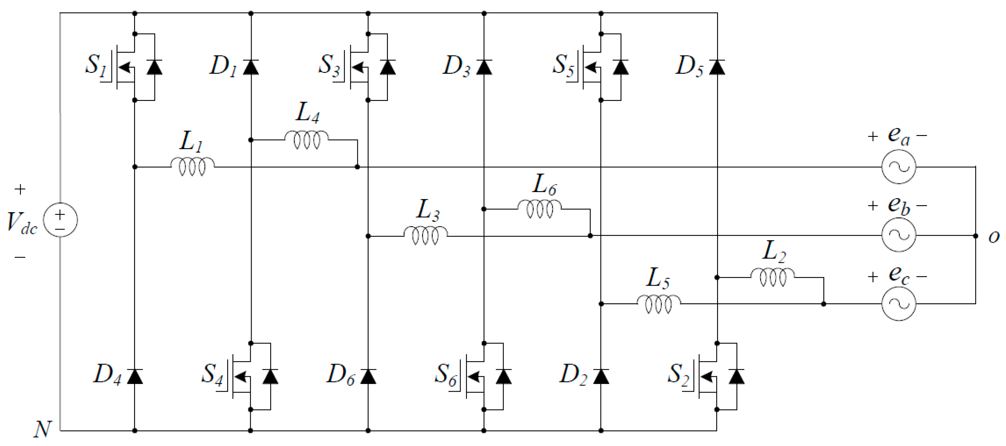
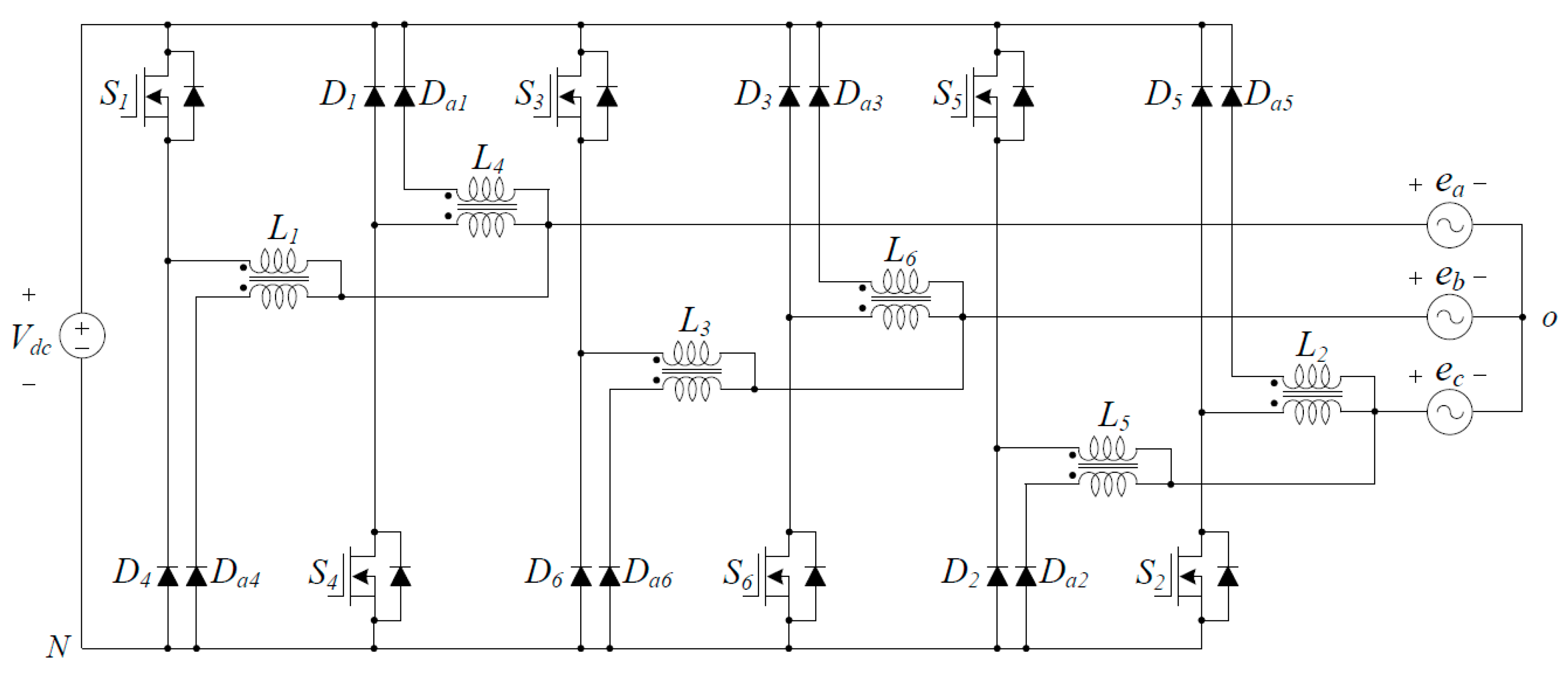
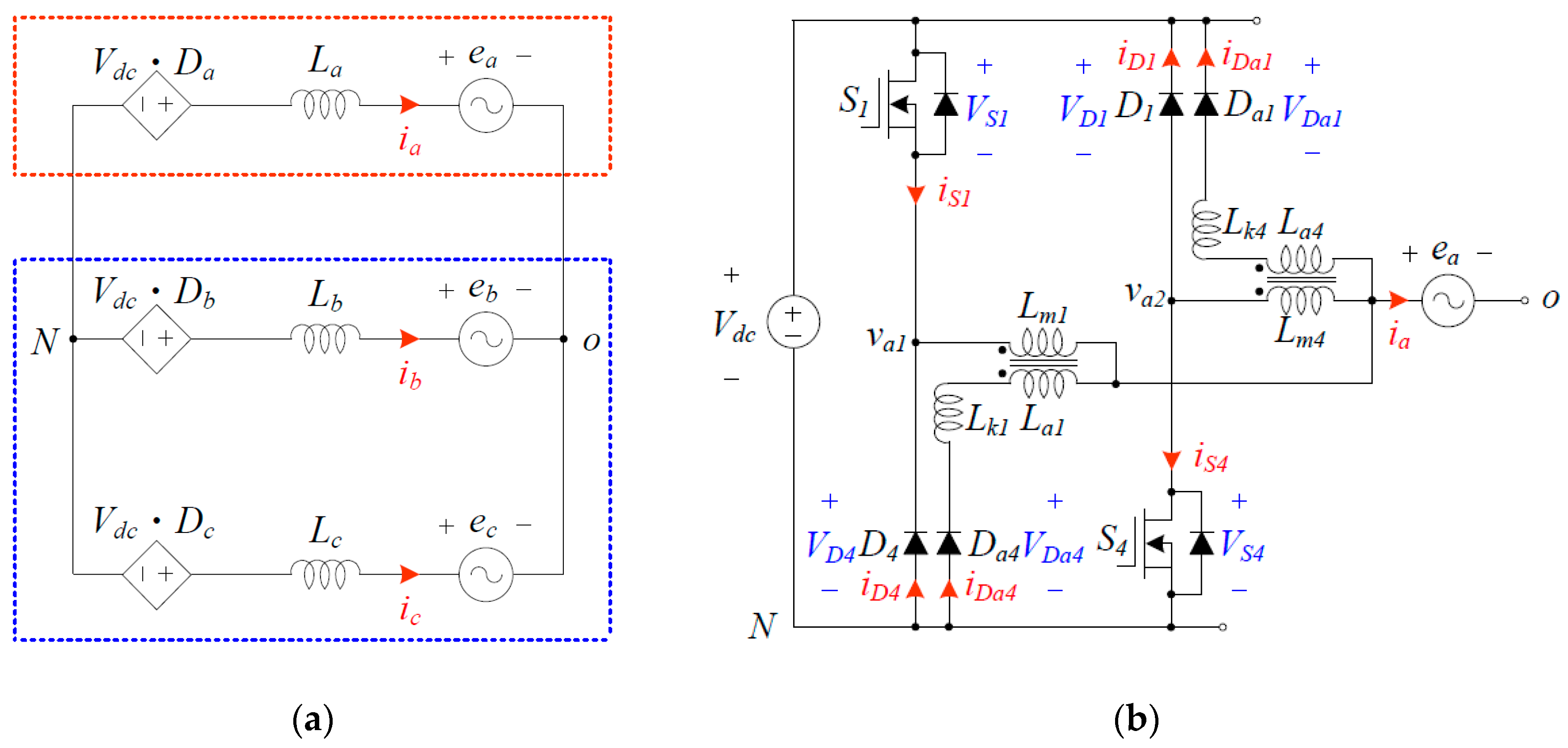
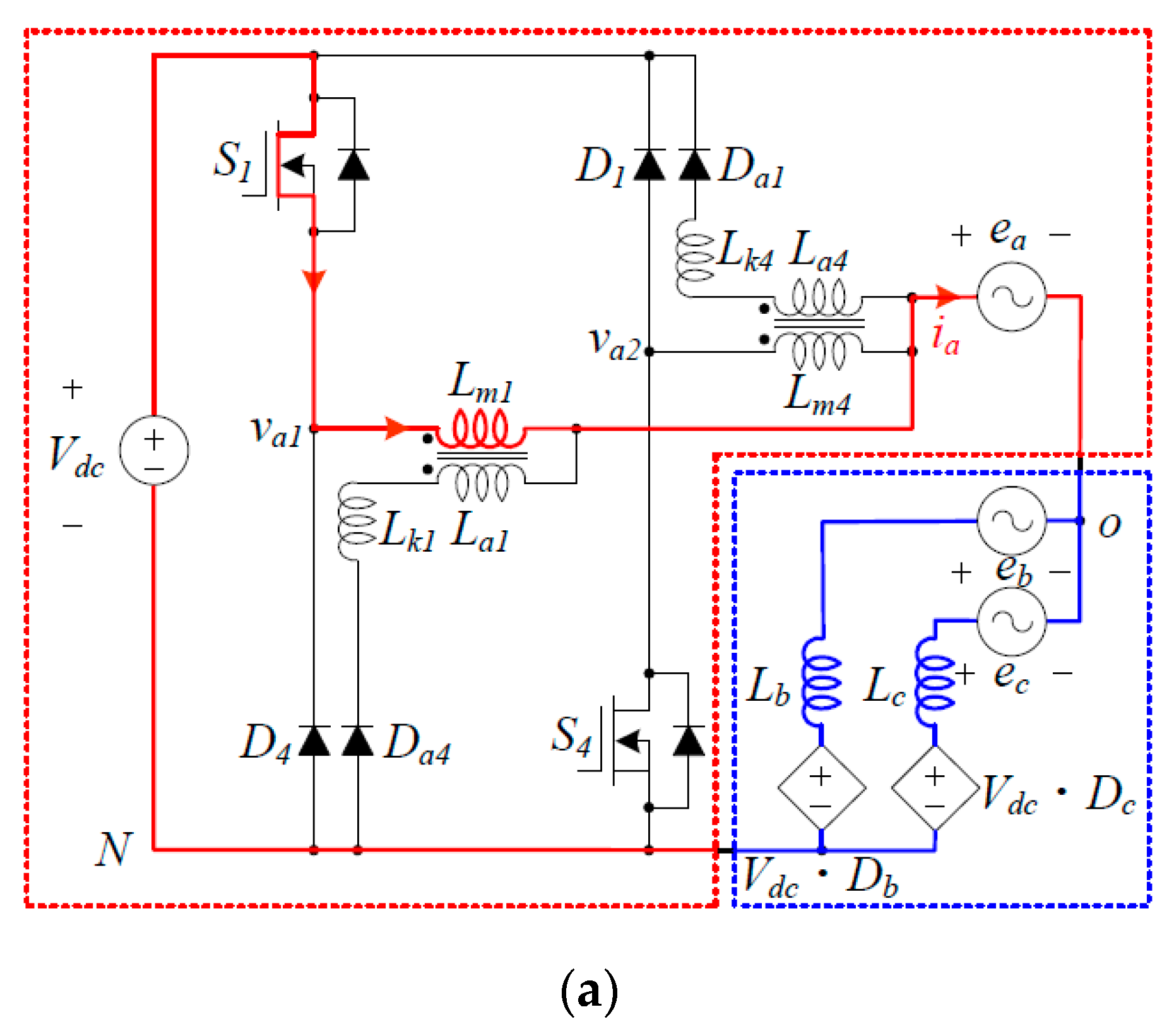
2. Proposed Inverter

2.1. Inverter Configuration

Figure 2 shows the circuit diagram of the proposed inverter. The proposed inverter consists of SiC MOSFETs (S1~S6), SiC schottky diodes (D1~D6), auxiliary SiC schottky diodes (Da1~Da6), and coupled inductors (L1~L6). The main and auxiliary windings of each coupled inductor are connected together. They are also connected to the mid-junction of each switching leg. Vdc is the dc-link voltage. N is the negative dc-link voltage. ea, eb, and ec are the phase voltage. o is the neutral point of the three-phase voltage. Dead-time is not necessary because when S1 operates, S4 is always turned off and vice versa. The output waveforms are more sinusoidal, and the energy is transferred more perfectly without the dead-time compensation. Assumed that the switching frequency is much higher than the grid frequency, the three-phase switching legs can be considered as three-phase voltage-controlled voltage-sources. Its equivalent switching-cycle average model can be derived, as shown in Figure 3a. In Figure 3a, Da, Db, and Dc are the duty ratio for switches S1, S3, and S5, respectively. ia, ib, and ic are the phase current, respectively. Figure 3b shows the circuit diagram for A-phase, which shows the reference directions of currents and voltages. The circuit diagram in Figure 3b can be applies to the B-phase and C-phase equivalently. The coupled inductors are modeled as a combination of the magnetizing inductors (Lm1~Lm6), auxiliary winding inductors (La1~La6), and leakage inductors (Lk1~Lk6). The auxiliary winding has a slightly larger number of turns than does the main winding. The leakage inductors are considered to be at the auxiliary winding of the coupled inductor.

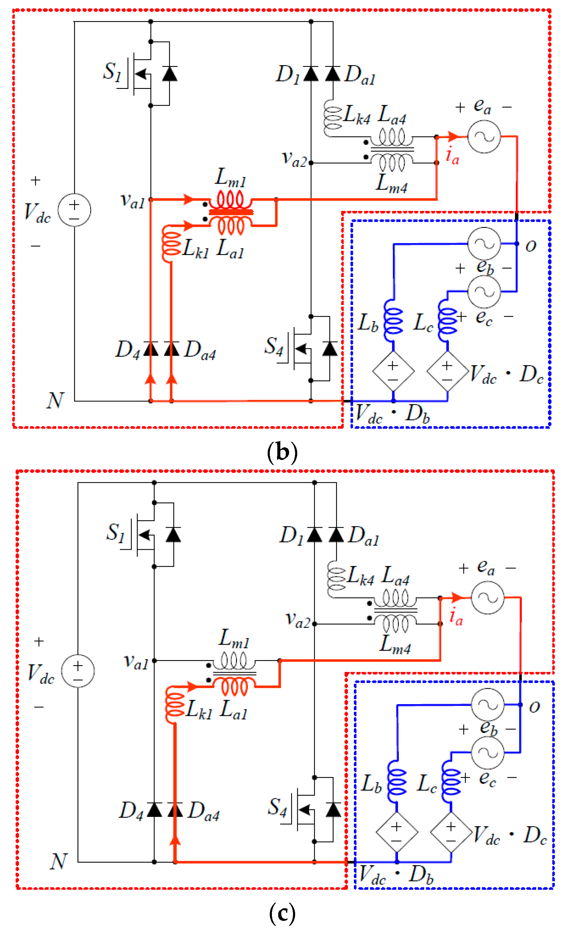
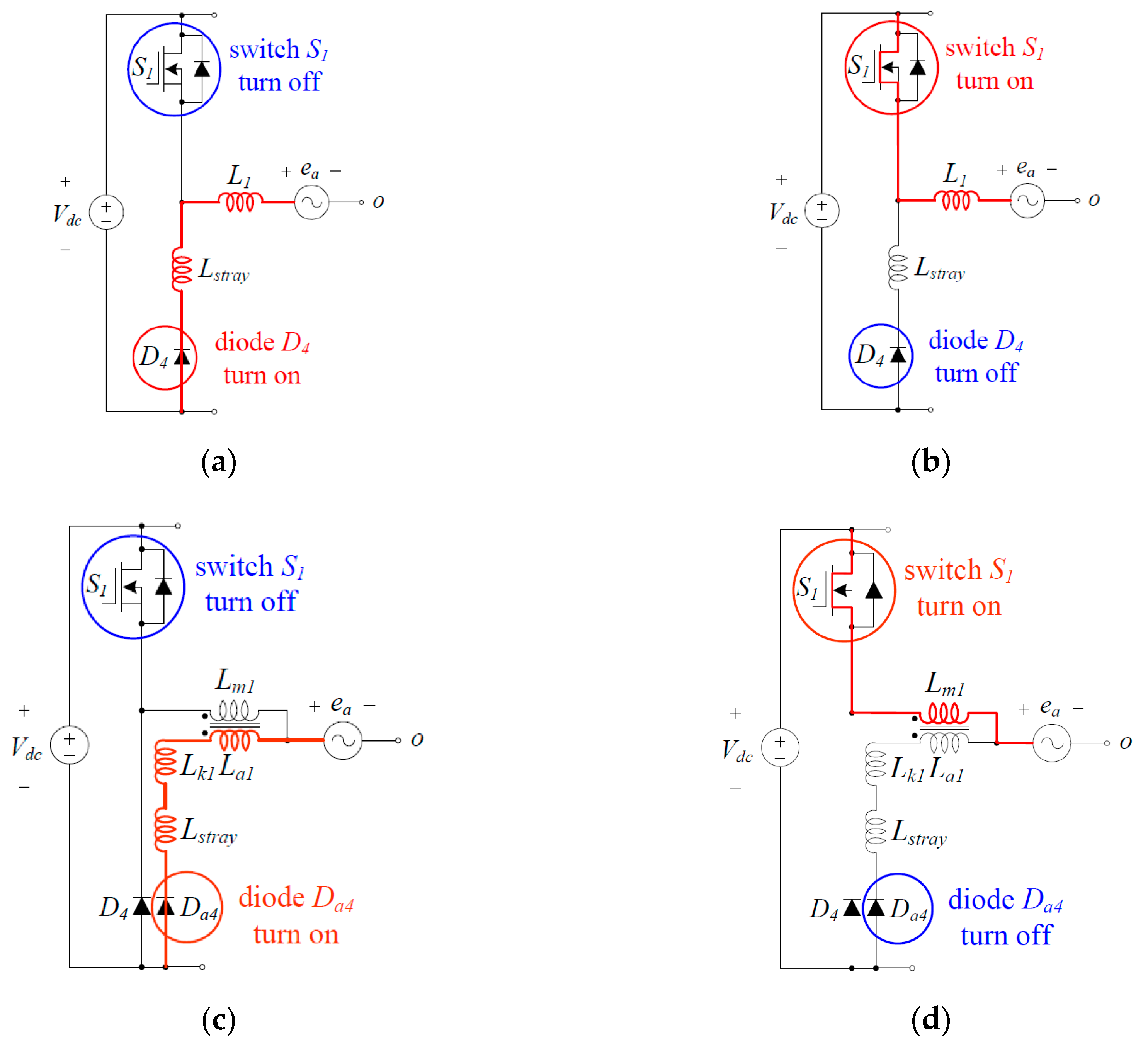
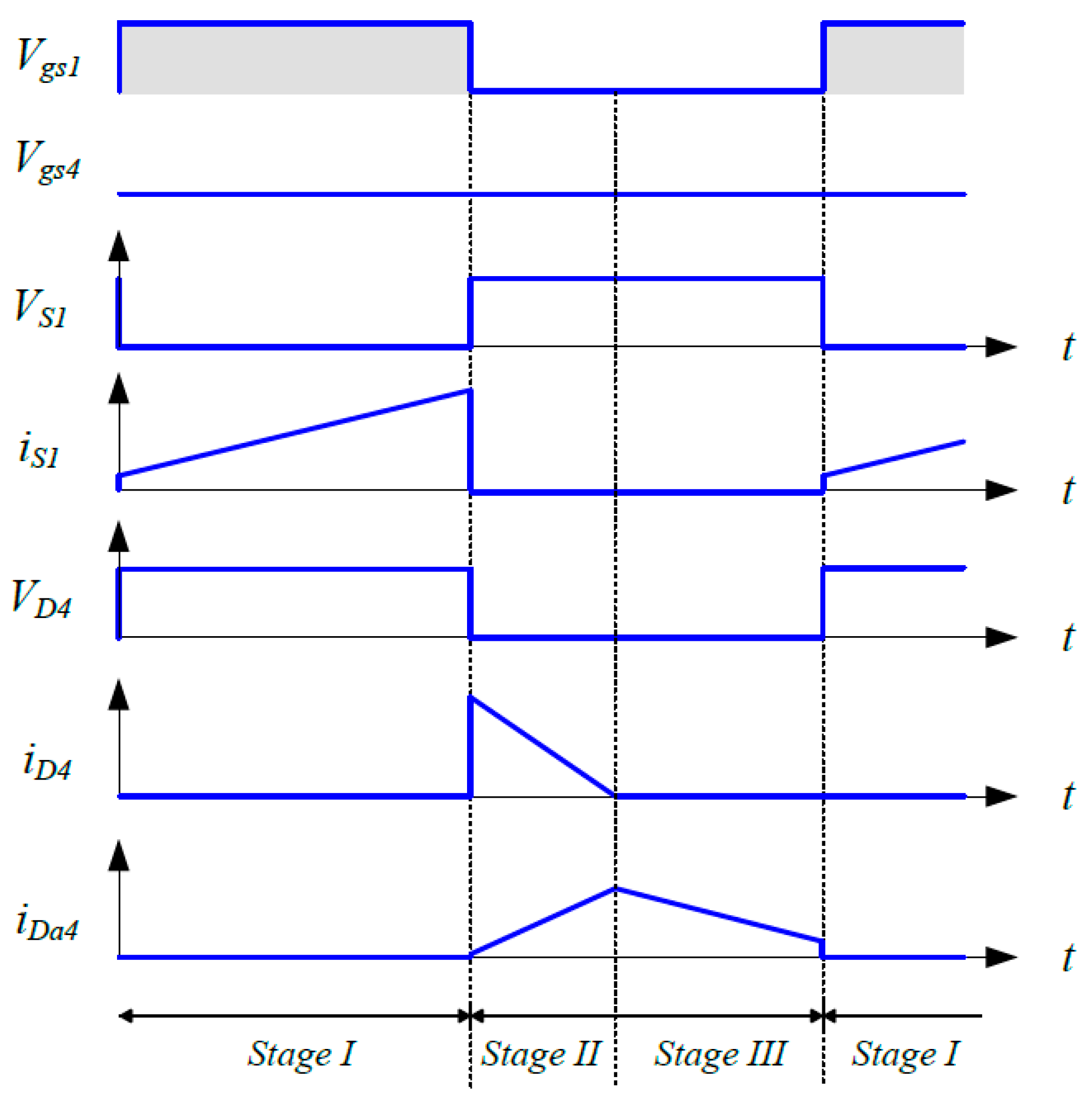
2.2. Steady-State Operation

Figure 4 shows switching-circuit diagrams of the proposed inverter during one switching period Ts for the positive cycle of the phase voltage ea. The operations of switching devices are determined by the phase current. Take A-phase, for example; when ia is positive, S1, D4, and Da4 are the operating devices, and when ia is negative, S4, D1, and Da1 are the operating devices. Figure 5 shows the steady-state operation waveforms during Ts for the positive cycle of the phase voltage ea. Stage I, Stage II, and Stage III in Figure 4 represent the current paths when ia is positive. Figure 5 shows the corresponding steady-state operation waveforms when ia is positive.
In Stage I, the switch S1 is turned on and the diodes D4 and Da4 are turned off. When S1 is turned on, the energy of the magnetizing inductor Lm1 is linearly charged by the dc-link voltage Vdc. Since diodes D4 and Da4 are reverse-biased, L1 operates like a simple inductor even though it is a coupled inductor. The phase current ia flows through Vdc, S1, Lm1, and ea. In this Stage I, the auxiliary winding of the coupled inductor L1 does not work.
In Stage II, the switch S1 is turned off and the diodes D4 and Da4 are turned on. Because S1 is turned off, the energy stored in the magnetizing inductor Lm1 is released to the output side through the main diode D4 and auxiliary diode Da4. In this Stage II, both main and auxiliary windings of the coupled inductor L1 work. When S1 is turned off, the main diode D4 is immediately turned on by the inductor current freewheeling. By the auxiliary winding of the coupled inductor L1, the voltage across the auxiliary winding is produced in an ideal turns ratio relationship. Then, auxiliary diode Da4 is turned on. The phase current ia flows through Lm1, ea, and D4. Simultaneously, ia flows through La1, ea, Da4, and Lk1. Because the auxiliary winding of the coupled inductor L1 has a slightly larger number of turns than does the main winding, a positive voltage is applied to the leakage inductor Lk1. The current of the main diode D4 keeps decreasing to zero current and the current through Lk1 increases linearly. The current-shifting process from the main diode D4 to the auxiliary diode Da4 begins.
In Stage III, the main diode D4 is turned off and auxiliary diode Da4 is still turned on. If the leakage inductor Lk1 is provided with sufficient charge voltage and time, the phase current ia is completely shifted to the new branch through diode Da4. Since switch S1 is still turned off and current of the main diode D4 is zero, L1 operates like a simple inductor even though it is a coupled inductor, and no current flows through Lm1. By the operation of coupled inductor, the main diode current is shifted to the auxiliary diode without the reverse-recovery process. The auxiliary diode current iDa4 decreases linearly. This switching state ends when S1 is turned on again.
The steady-state operation for the negative cycle of the phase voltage ea is not descried here, because it can be explained similarly to the steady-state operation of the positive cycle of the phase voltage ea.
Since the phase currents flow simultaneously, the steady-state operation principle applies to the B-phase and C-phase. For the B-phase, when ib is positive, S3, D6, and Da6 are the operating devices, and when ib is negative, S6, D3, and Da3 are the operating devices. For the C-phase, when ic is positive, S5, D2, and Da2 are the operating devices, and when ic is negative, S2, D5, and Da5 are the operating devices. For each switching leg, by using only one auxiliary diode and adding one coupled winding to the inductor, the current through the original diode can be steered to an auxiliary diode and can be reduced to zero before the switch turns on. The leakage inductor of the coupled inductor is used to control the di/dt.
In a practical design, the SiC schottky diodes suffer from significant current overshoots and voltage oscillations due to the resonance of RLC circuit formed by the diode parasitic resistance, stray inductance, and diode capacitance. Figure 6 shows the switching characteristic of the SiC schottky diode for one switching-leg. Lstray is the parasitic stray inductance. Figure 6a,b show the switching characteristic of the conventional inverter when the diode D4 is turned on and turned off, respectively. Figure 6c,d show the switching characteristic of the proposed inverter when the diode Da4 is turned on and turned off, respectively. The steady-state operation of the proposed inverter is changed from Stage III to Stage I. In the conventional inverter, when the switch has started operating again as shown Figure 6b, the parasitic capacitances of the switch and the parasitic RLC circuit of the diode D4 including Lstray resonate within the switching leg. Thus, the switch peak current and diode reverse-recovery peak current are quite high. These high currents cause switching-power losses, which reduce the power efficiency. On the other hand, in the proposed inverter, before the switch is turns on, the current through the original diode is already zero and the switch current flows through the magnetizing inductor. Thus, the reverse-recovery peak current and reverse-recovery time of the main diode are reduced. The current rising rate of the switch will be lowered, which can reduce the turn-on switching-power loss of the switch. Also, the current through the auxiliary diode at the end of Stage III can be limited by the leakage inductor of the auxiliary winding. Therefore, the reverse-recovery peak current and reverse-recovery time of the auxiliary diode are also reduced.

2.3. Contol and Modulation

The proposed inverter provides smooth powering and controls the phase currents ia, ib, and ic for the unity power factor. The phase voltages ea, eb, and ec are expressed as
e a = E cos ( ω t ) ,
e b = E cos ( ω t 2 3 π ) ,
e c = E cos ( ω t 4 3 π )
where E is the maximum phase voltage and ω is angular frequency. The phase-leg voltages vao, vbo, and vco are expressed as
v i o = { v i 1 when v i o > 0 v i 2 when v i o 0
where i = a, b, c. The voltage equations in the stationary a-b-c frame are
e a = L d i a d t + v a o ,
e b = L d i b d t + v b o ,
e c = L d i c d t + v c o
where coupled inductor L (=L1~L6) has the same value. The voltage equations in the synchronous d-q frame are
[ e d e q ] = [ cos ( ω t ) sin ( ω t ) sin ( ω t ) cos ( ω t ) ] 2 3 [ 1 1 2 1 2 0 3 2 3 2 ] [ e a e b e c ] = [ cos ( ω t ) sin ( ω t ) sin ( ω t ) cos ( ω t ) ] ( L d d t ) [ cos ( ω t ) sin ( ω t ) sin ( ω t ) cos ( ω t ) ] 1 [ i d i q ] + [ v d v q ] = L d d t [ i d i q ] ω L [ i q i d ] + [ v d v q ] .
The grid voltages of the synchronous d-q frame are ed = E and eq = 0. For the unity power factor, it is desirable that the iq be zero. Then iq is controlled with the zero reference current iq* = 0. The voltage equations from (5) to (7) are transformed from the stationary a-b-c frame to the synchronous d-q frame as follows
E = L d i d d t + ω L i q + v d ,
0 = L d i q d t ω L i d + v q .
The proportional and integral-type controllers do not work well as rapid tracking controllers in (9) and (10). To solve this problem, the following decoupling control is used as
v d = E ω L i q + Δ v d ,
v q = ω L i d + Δ v q
with the addition of the current controller (11) and (12) to the inverter (9) and (10), respectively, the input-output relations of the inverter become first-order decoupled linear systems as
0 = L d i d d t + Δ v d ,
0 = L d i q d t + Δ v q
where the output signals Δvd and Δvq of the current controllers
Δ v d = k p d ( i d * i d ) + k i d ( i d * i d ) d t ,
Δ v q = k p q ( i q * i q ) + k i q ( i q * i q ) d t
where kpd and kpq are proportional control gains and kid and kiq are integral control gains, respectively. In terms of the conduction times Ta, Tb, and Tc of switches S1, S3, and S5, the voltages vaN, vbN, and vcN are expressed as
v a N = V d c T s T a ,
v b N = V d c T s T b ,
v c N = V d c T s T c .
The neutral-point voltage voN of the balanced three-phase system is obtained by the superposition theorem as
v o N = 1 3 V d c T s ( T a + T b + T c ) .
The relation of the stationary a-b-c voltage components and the conduction times of switches are derived as
[ v a o v b o v c o ] = [ v a N v o N v b N v o N v c N v o N ] = 1 3 V d c T s [ 2 1 1 1 2 1 1 1 2 ] [ T a T b T c ] .
In Region 1, substituting Tc = 0 into equation (21) when using V0 (0 0 0) as the zero vector, the conduction times of switches are obtained as
[ T a T b T c ] = T s V d c [ v a o v c o v b o v c o 0 ]
where the stationary a-b-c voltage components are given by
[ v a o v b o v c o ] = [ 1 0 1 2 3 2 1 2 3 2 ] [ cos ω t sin ω t sin ω t cos ω t ] [ v d v q ] .
Applying a similar procedure to all regions, the conduction times of switches for modulating the required space vector are simplified as
[ T a T b T c ] = T s V d c [ v a o v min v b o v min v c o v min ] = [ T s T s T s ] [ v max v a o v max v b o v max v c o ]
where vmin = min (vao, vbo, vco) and vmax = max (vao, vbo, vco). Figure 7 shows the control block diagram of the proposed inverter. The conduction times Ta, Tb, and Tc of switches S1, S3, and S5 for three-phase PWM pulses are generated by the space-vector modulation technique without a computational burden such as square root and arctangent.

3. Simulation and Experimental Results

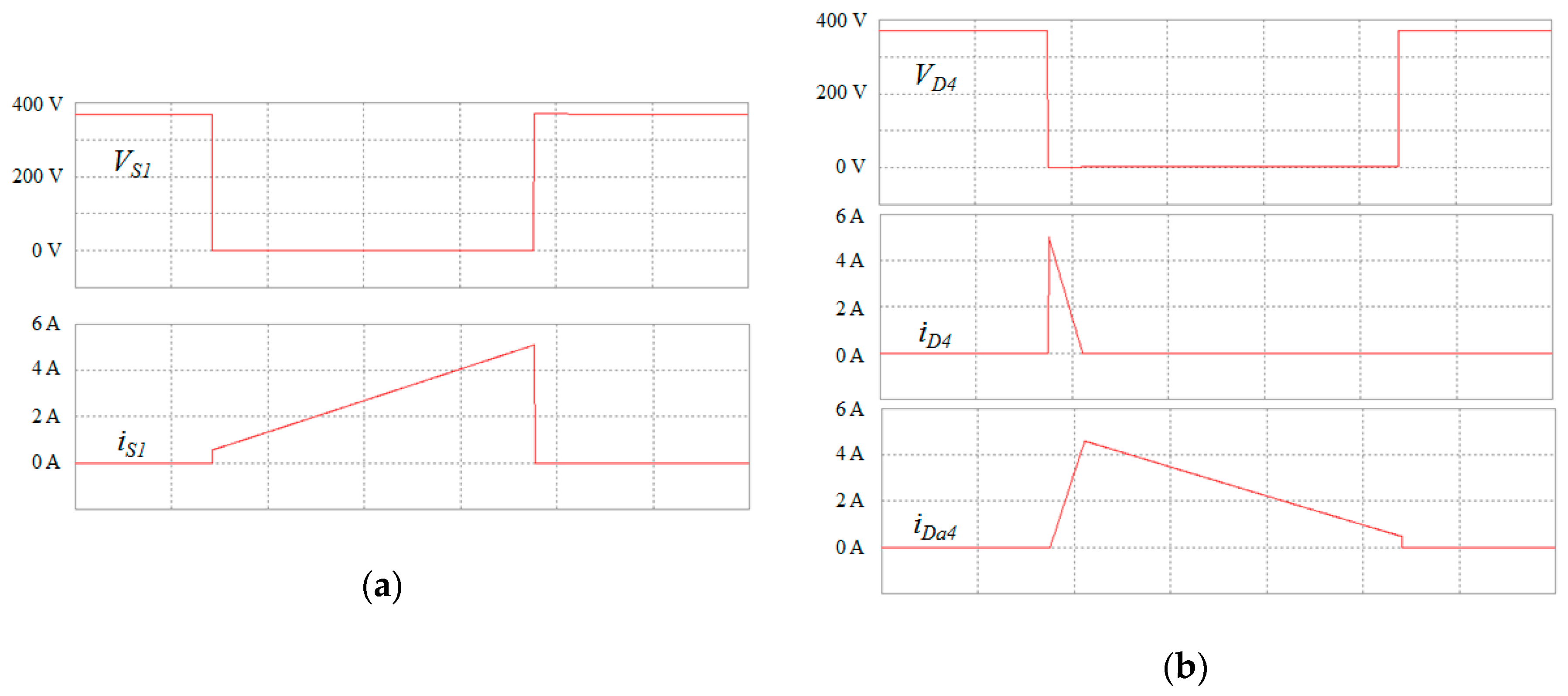
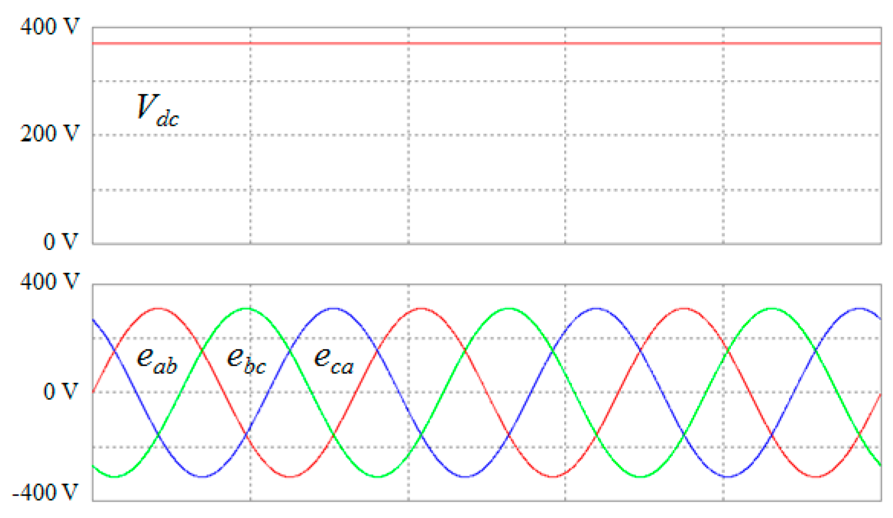
3.1. Simulation Results

We executed a computer simulation for steady-state operation of the conventional inverter and the proposed inverter by using Physical Security Information Management (PSIM) software [21]. Table 1 shows the electrical specifications of the inverters. The dc-link voltage Vdc should be higher than the peak line-to-line voltage of the inverter. Then, the inverters will require minimum dc-link voltage of 311 V. In addition, the voltage margin, modulation index, and device voltage rating must be taken into account. Thus, we selected the dc-link voltage of 370 V.
Figure 8 shows the simulation results of the conventional inverter in Figure 1 when Vdc is 370 V, ea, eb, and ec are 127 Vrms. Figure 8a shows VS1 and iS1. Figure 8b shows VD4 and iD4. As shown in Figure 8a,b, VS1 and VD4 are clamped to Vdc, and the slope of iS1 and iD4 is opposite.
Figure 9 and Figure 10 show the simulation results of the proposed inverter when Vdc is 370 V, ea, eb, and ec are 127 Vrms. Figure 9a shows VS1 and iS1. Figure 9b shows VD4, iD4, and iDa4. As shown in Figure 9a,b, the VS1 and VD4 are clamped to Vdc and the current through the original diode can be steered to an auxiliary diode and can be reduced to zero before the switch turns on. Figure 10 shows eab, ebc, eca, and Vdc. Balanced line-to-line voltages are equal in magnitude and frequency and out of phase with each other by 120°.

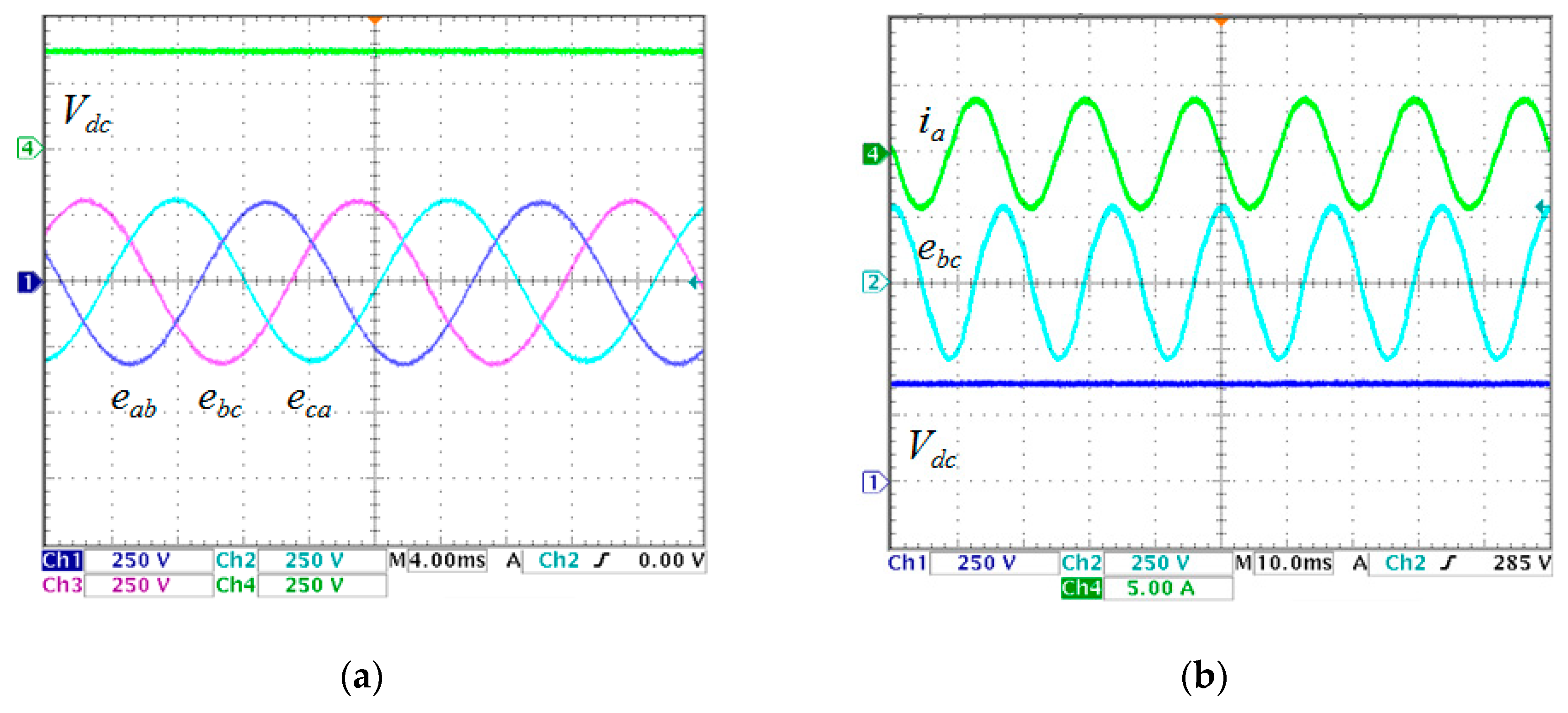
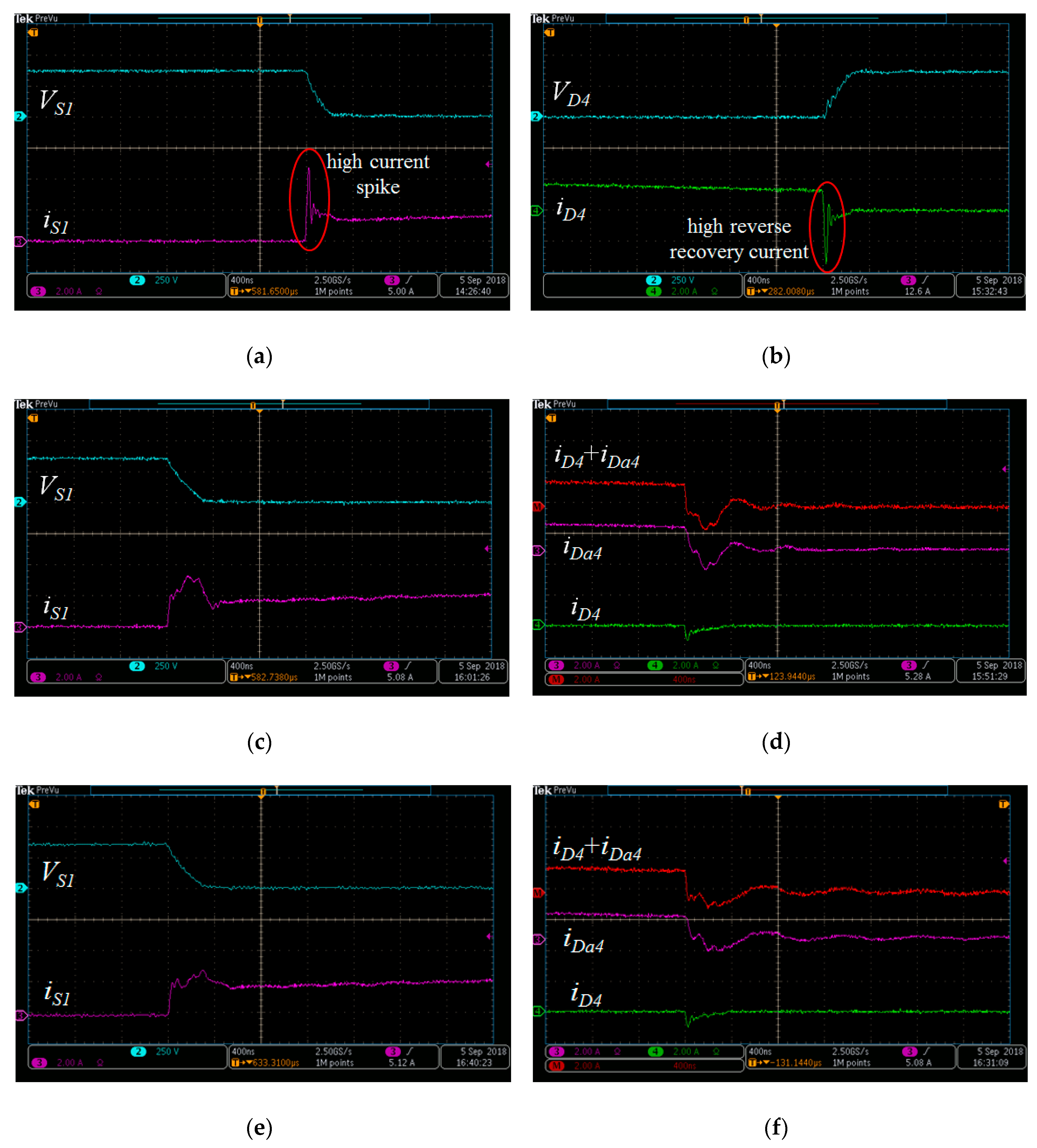
3.2. Experimental Results

To evaluate the performance of the proposed inverter, we built and tested a 1.0 kW prototype inverter. The conventional inverter was also designed for the performance comparison with the proposed inverter. The electrical specifications of the prototype inverter are shown in Table 1. Table 2 shows the component parameters of the prototype inverter. The hardware prototype is divided into two parts: the microprocessor-based control circuit and the power circuit. We have implemented the control block diagram of the proposed inverter, as shown in Figure 7, by using a dsPIC30F6015 (Microchip Technology, Chandler, AZ, USA) 16-bit fixed point digital signal controller. We have measured the signals using an analog to digital converter in the microprocessor. The controllers have been executed for every sample period of 100 μs.
Figure 11 shows the experimental waveforms of the conventional inverter in Figure 1 when Vdc is 370 V, and ea, eb, and ec are 127 Vrms. Figure 11a shows VS1 and iS1. Figure 11b shows VD4 and iD4. The switch peak current and diode reverse-recovery peak current are quite high. As shown in Figure 11a,b, switching-power losses related to switch current and diode reverse-recovery current are increased, reducing the power efficiency of the inverter.
Figure 12 shows the experimental waveforms of the proposed inverter in Figure 2 when Vdc is 370 V, and ea, eb, and ec are 127 Vrms. Figure 12a shows VS1 and iS1. Figure 12b shows VD4 and iD4. As shown in Figure 12a,b, the switch peak current and diode reverse-recovery peak current are reduced, as is the reverse-recovery time. Therefore, switching-power loss related to the switch current and diode reverse-recovery current are dramatically reduced. Figure 12c shows iD4 + iDa4, iD4 and iDa4 with Lk = 5 µH. Figure 12d shows iD4 + iDa4, iD4 and iDa4 with Lk = 15 µH. As shown in Figure 12c,d, the experimental waveforms show the significant performance improvement attained by controlling the diode di/dt.
Figure 13 shows the experimental waveforms of the conventional inverter in Figure 1 and the proposed inverter in Figure 2 when Vdc is 370 V, and ea, eb, and ec are 127 Vrms. Figure 13a shows VS1 and iS1 in the conventional inverter of the enlarged Figure 11a. Figuere 13b shows VD4 and iD4 in the conventional inverter of the enlarged Figure 11b. We observed in Figure 13a,b that there is a high switch current spike and the diode reverse-recovery current is increased, as shown in Figure 11a,b, which reduces the power efficiency of the inverter. Especially, Figure 13b shows significant output oscillations of the SiC schottky diode, which result from the ringing formed between the diode parasitic capacitance, parasitic stray inductance, and diode resistance. Figure 13c shows VS1 and iS1 with Lk = 5 µH in the proposed inverter of the enlarged Figure 12a. Figure 13d shows iD4 + iDa4, iD4 and iDa4 with Lk = 5 µH in the proposed inverter of the enlarged Figure 12c. Figure 13e shows VS1 and iS1 with Lk = 15 µH in the proposed inverter. Figure 13f shows iD4 + iDa4, iD4 and iDa4 with Lk = 15 µH in the proposed inverter of the enlarged Figure 12d. We observed from Figure 13c to 13f that the switch peak current and diode reverse-recovery peak current are reduced, as is the reverse-recovery time, as shown in Figure 12a,b. Also, the current oscillation has been much alleviated because the current through the original diode can be steered to an auxiliary diode by using magnetically coupled inductors.
Figure 14 shows the experimental waveforms of the proposed inverter when Vdc is 370 V, ea, eb, and ec are 127 Vrms. Figure 14a shows eab, ebc, eca, and Vdc. Balanced line-to-line voltages are equal in magnitude and frequency and out of phase with each other by 120°. Figure 14b shows ia, ebc, and Vdc for a 1.0 kW output power.
Figure 15 shows the measured power efficiencies for the conventional inverter in Figure 1, the proposed inverter with Lk = 5 µH, and the proposed inverter with Lk = 15 µH, respectively. Figure 15a shows the power efficiencies of the inverters for different output power levels when Vdc is 370 V, and ea, eb, and ec are 127 Vrms. The conventional inverter has the power efficiency of 97.6% at the rated power. On the other hand, the proposed inverter with Lk = 5 µH has improved power efficiency, achieving a power efficiency of 98.0% at the rated power. The proposed inverter improves the power efficiency by 0.4% compared to the conventional inverter by using magnetically coupled inductor switching technique. The proposed inverter with Lk = 15 µH has achieved a power efficiency of 98.2% for a 1.0 kW output power. Figure 15b shows the power efficiencies of the proposed inverter for different leakage inductances when Vdc is 370 V, and ea, eb, and ec are 127 Vrms. The leakage inductances of the proposed inverter have major impact on the results. As shown in Figure 15b, the proposed inverter with Lk = 15 µH has achieved the highest efficiency compared to the extra leakage inductance. Both the proposed inverter with Lk = 10 µH and Lk = 20 µH have achieved a power efficiency of 98.1% at the rated power. If the leakage inductance is lower than 5 µH, the proposed inverter does not operate normally. On the other hand, if the leakage inductance is higher than 15 µH, the conduction loss of the coupled inductor increases, decreasing the power efficiency. The minimum value of the leakage inductance that the proposed inverter can operate normally is 5 µH, and the maximum value of the leakage inductance that the proposed inverter can achieve high efficiency is 15 µH. Figure 15c shows the power efficiencies of the inverters for different dc-link voltage levels at the rated power. As shown in Figure 15c, the maximum power efficiency of the inverters is dc-link voltage of 370 V at the rated power. If the dc-link voltage is lower than 370 V, the modulation index is very high. High modulation index causes switching-power loss, decreasing the power efficiency. On the other hand, if the dc-link voltage is higher than 370 V, the voltage stress of switching devices is very high. The use of high-rating switching devices causes the high cost as well as low efficiency.

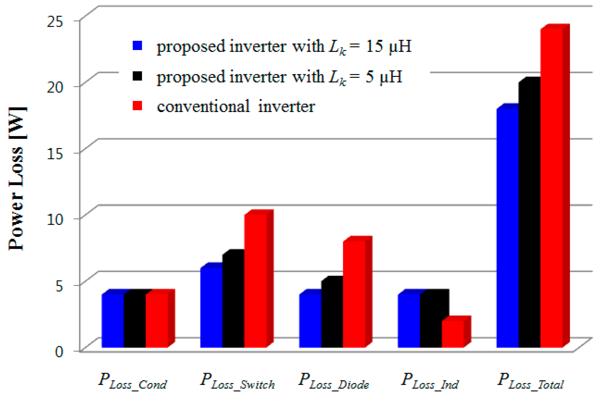
3.3. Power Loss Analysis

In order to analysis the power loss for a switching device, switching characteristics are presented, as shown in Figure 16. Figure 16a shows the switching waveforms and instantaneous switching-power loss. During the turn-on transition of the switching device, the current build-up consists of a short delay time td(on) followed by the current rise time tri. The voltage falls to a small on-state value of Von with a voltage fall time of tfv. Then, the energy dissipated in the device during this turn-on transition can be approximated as
W c ( o n ) 1 2 V I t c ( o n )
where it is recognized that no energy dissipation occurs during the turn-on delay interval td(on). During the turn-off transition period of the switching device, the voltage build-up consists of a turn-off delay time td(off) and a voltage rise time trv. The current falls to zero with a current fall time tfi. Then, the energy dissipated in the device during this turn-off transition can be written as
W c ( o f f ) 1 2 V I t c ( o f f )
where any energy dissipation during the turn-off delay interval td(off) is ignored since it is small compared to Wc(off). Therefore, the average switching-power loss Ps because of these transitions can be approximated from (25) and (26) as
P s = 1 2 V I f s ( t c ( o n ) + t c ( o f f ) ) .
Figure 16b shows the current waveform for a power diode. The time interval trr is the reverse-recovery time, the current Irr is the reverse-recovery current, iF is forward current, and iR is the reverse current. Therefore, reverse-recovery charge Qr can be approximated as
Q r 1 2 I r r t r r .
Figure 17 compares the loss breakdown plots of the inverters for a 1.0 kW output power. The proposed inverter with Lk = 15 µH achieves the power efficiency of 98.2% at 1.0 kW, resulting in power losses of 18 W. The proposed inverter with Lk = 5 µH achieves the power efficiency of 98.0%, resulting in power losses of 20 W. On the other hand, the conventional inverter achieves the power efficiency of 97.6%, resulting in power losses of 24 W. PLoss_Cond is the conduction losses of switching devices including SiC MOSFETs and SiC schottky diodes. PLoss_Switch is the switching losses of the SiC MOSFETs. PLoss_Diode is the reverse-recovery loss of the SiC schottky diodes. PLoss_Ind is the core losses of the coupled inductors. PLoss_Total is the total power losses. The core losses of the proposed inverter because of the coupled inductors are high compared with those of the conventional inverter. However, the switching losses and the reverse-recovery losses of the proposed inverter are reduced remarkably.
Table 3 shows the comparison results of different approaches for reducing switching-power losses. It shows that the required components in each switching leg, advantages, and drawbacks. Compared with the proposed inverter, the RC snubber in [13] has a simple structure and low cost, but its efficiency very low because it dissipates the switching-power loss in the resistor. Passive lossless snubber in [14] can achieve zero-current turn on and zero-voltage turn off, but it requires many components and increases system complexity. Moreover, additional feedback circuit is required. Undeland snubber in [15] has a relatively simple structure, but it requires additional circuits of regenerative and dissipative. Active-clamping circuit in [16] provides zero-voltage switching conditions for all switches, but voltage stress of power devices is increased higher than the dc-link voltage. The use of high-rating switching devices causes the high cost as well as low efficiency. The proposed inverter is compared with the recently presented approaches as well as the conventional approaches. Compared with the proposed inverter, the bus-side RCD snubber presented in [17] has the advantages of simple topology, high reliability, and low cost. However, the series resistor in the snubber circuit makes contributes to energy loss, similar to the reference [13]. The qZSI presented in [18] effectively reduced number of switch commutations, resulting in reduced switching-power losses. However, modulation methods of the qZSI are more complicated than the proposed inverter. The ZVS three-phase four-wire inverter presented in [19,20] can achieve the zero-voltage switching operation of all switches, including the main switches and the auxiliary switch. However, the voltage stress of power devices is higher than the input dc voltage, similar to the reference [16]. For such a reason, the proposed inverter is superior to other different approaches in the state of art.

4. Conclusions

We have proposed a three-phase SOI with SiC devices using magnetically coupled inductor switching. The proposed inverter improves the power efficiency by using a magnetically coupled inductor switching technique. The current through the original diode can be steered to a new branch to reduce the significant output oscillations of the conventional inverter. We have discussed the configuration, steady-state operation, control, and modeling of the proposed inverter. In addition, the proposed solution is compared not only with conventional solutions [13,14,15,16] but also with recent solutions [17,18,19,20]. The proposed solution reduces switching-power losses simply and effectively, compared to the previous solutions, which require additional circuits, complex modulation methods, and high voltage stresses of power device. We have designed and tested a 1.0 kW prototype inverter to verify the performance of the proposed inverter. The proposed inverter improves the power efficiency more than does the conventional inverter by alleviating the voltage oscillations of SiC schottky diodes.

Author Contributions

M.-K.Y. and W.-Y.C.; Data curation, M.-K.Y.; Project administration, W.-Y.C.; Supervision, W.-Y.C.; Writing–original draft, M.-K.Y.

Funding

This research was supported by the National Research Foundation of Korea (NRF-2016R1D1A3B03932350).

Conflicts of Interest

The authors declare no potential conflict of interest.

References

  1. Chen, M.; Xu, D.; Zhang, T.; Shi, K.; He, G.; Rajashekara, K. A Novel DC Current Injection Suppression Method for Three-Phase Grid-Connected Inverter Without the Isolation Transformer. IEEE Trans. Ind. Electron. 2018, 65, 8656–8666. [Google Scholar] [CrossRef]
  2. Afshari, E.; Moradi, G.R.; Rahimi, R.; Farhangi, B.; Yang, Y.; Blaabjerg, F.; Farhangi, S. Control Strategy for Three-Phase Grid-Connected PV Inverters Enabling Current Limitation Under Unbalanced Faults. IEEE Trans. Ind. Electron. 2017, 64, 8908–8918. [Google Scholar] [CrossRef]
  3. Kantar, E.; Hava, A.M. Optimal Design of Grid-Connected Voltage-Source Converters Considering Cost and Operating Factors. IEEE Trans. Ind. Electron. 2016, 63, 5336–5347. [Google Scholar] [CrossRef]
  4. Lewicki, A. Dead-Time Effect Compensation Based on Additional Phase Current Measurements. IEEE Trans. Ind. Electron. 2015, 62, 4078–4085. [Google Scholar] [CrossRef]
  5. Khan, A.A.; Cha, H. Dual-Buck-Structured High-Reliability and High-Efficiency Single-Stage Buck–Boost Inverters. IEEE Trans. Ind. Electron. 2018, 65, 3176–3187. [Google Scholar] [CrossRef]
  6. Yan, Q.; Yuan, X.; Geng, Y.; Charalambous, A.; Wu, X. Performance Evaluation of Split Output Converters With SiC MOSFETs and SiC Schottky Diodes. IEEE Trans. Power Electron. 2017, 32, 406–422. [Google Scholar] [CrossRef]
  7. Sun, P.; Liu, C.; Lai, J.-S.; Chen, C.-L.; Kees, N. Three-Phase Dual-Buck Inverter With Unified Pulsewidth Modulation. IEEE Trans. Power Electron. 2012, 27, 1159–1167. [Google Scholar] [CrossRef]
  8. Singh, R.; Cooper, J.A.; Melloch, M.R.; Chow, T.P.; Palmour, J.W. SiC power schottky and PiN diodes. IEEE Trans. Electron Devices. 2002, 49, 665–672. [Google Scholar] [CrossRef]
  9. Biela, J.; Schweizer, M.; Waffler, S.; Kolar, J.W. SiC versus Si—Evaluation of Potentials for Performance Improvement of Inverter and DC–DC Converter Systems by SiC Power Semiconductors. IEEE Trans. Ind. Electron. 2011, 58, 2872–2882. [Google Scholar] [CrossRef]
  10. Oswald, N.; Anthony, P.; McNeill, N.; Stark, B.H. An Experimental Investigation of the Tradeoff between Switching Losses and EMI Generation With Hard-Switched All-Si, Si-SiC, and All-SiC Device Combinations. IEEE Trans. Power Electron. 2014, 29, 2393–2407. [Google Scholar] [CrossRef]
  11. Ho, C.N.-M.; Breuninger, H.; Pettersson, S.; Escobar, G.; Canales, F. A Comparative Performance Study of an Interleaved Boost Converter Using Commercial Si and SiC Diodes for PV Applications. IEEE Trans. Power Electron. 2013, 28, 289–299. [Google Scholar] [CrossRef]
  12. Alatise, O.; Parker-Allotey, N.-A.; Hamilton, D.; Mawby, P. The Impact of Parasitic Inductance on the Performance of Silicon–Carbide Schottky Barrier Diodes. IEEE Trans. Power Electron. 2012, 27, 3826–3833. [Google Scholar] [CrossRef]
  13. Salem, T.E.; Wood, R.A. 1000-H Evaluation of a 1200-V, 880-A All-SiC Dual Module. IEEE Trans. Power Electron. 2014, 29, 2192–2198. [Google Scholar] [CrossRef]
  14. Zhang, H.; Wang, Q.; Chu, E.; Liu, X.; Hou, L. Analysis and Implementation of A Passive Lossless Soft-Switching Snubber for PWM Inverters. IEEE Trans. Power Electron. 2011, 26, 411–426. [Google Scholar] [CrossRef]
  15. Sperb, J.D.; Zanatta, I.X.; Michels, L.; Rech, C.; Mezaroba, M. Regenerative Undeland Snubber Using a ZVS PWM DC–DC Auxiliary Converter Applied to Three-Phase Voltage-Fed Inverters. IEEE Trans. Ind. Electron. 2011, 58, 3298–3307. [Google Scholar] [CrossRef]
  16. Mezaroba, M.; Martins, D.C.; Barbi, I. A ZVS PWM three-phase inverter with active clamping technique using the reverse recovery energy of the diodes. In Proceedings of the IEEE Annual Power Electronics Specialists Conference (PESC, 2004), Aachen, Germany, 20–25 June 2004; pp. 4785–4790. [Google Scholar]
  17. Lee, Y.K.; Kim, J.K.; Cho, E.S. Design of Bus-Side RCD Snubber Circuit for Three-Phase High-Power Inverters. Can. J. Electr. Comput. Eng. 2018, 41, 55–61. [Google Scholar]
  18. Abdelhakim, A.; Davari, P.; Blaabjerg, F.; Mattavelli, P. Switching Loss Reduction in the three-Phase Quasi-Z-Source Inverters Utilizing Modified Space Vector Modulation Strategies. IEEE Trans. Power Electron. 2018, 33, 4045–4060. [Google Scholar] [CrossRef]
  19. He, N.; Zhu, Y.; Zhao, A.; Xu, D. Zero-Voltage-Switching Sinusoidal Pulsewidth Modulation Method for Three-Phase Four-Wire Inverter. IEEE Trans. Power Electron. 2019, 34, 7192–7205. [Google Scholar] [CrossRef]
  20. Shi, K.; Zhao, A.; Deng, J.; Xu, D. Zero-Voltage-Switching SiC-MOSFET Three-Phase Four-Wire Back-to-Back Converter. IEEE J. Emerging Sel. Top. Power Electron. 2019, 7, 722–735. [Google Scholar] [CrossRef]
  21. Powersim Inc. PSIM User’s Guide, Version 9.0, Release2. 2010. Available online: https://www.google.com.hk/url?sa=t&rct=j&q=&esrc=s&source=web&cd=2&cad=rja&uact=8&ved=2ahUKEwiPzOnG6pjkAhWi3mEKHedFD8YQFjABegQIBxAC&url=https%3A%2F%2Fwww.myway.co.jp%2Fproducts%2Fpsim%2Fdlfiles%2Fpdf%2FPSIM_User_Manual_V9.0.2.pdf&usg=AOvVaw0PXhhbMuDyBD5tERrVhvAl (accessed on 1 March 2010).
Figure 1. Circuit diagram of the conventional three-phase split-output inverter.
Electronics 08 00969 g001
Figure 2. Circuit diagram of the proposed inverter.
Electronics 08 00969 g002
Figure 3. Switching-cycle average model and circuit diagram of the proposed inverter with reference directions of currents and voltages for A-phase: (a) switching-cycle average model; (b) circuit diagram for A-phase.
Electronics 08 00969 g003
Figure 4. Switching-circuit diagrams of the proposed inverter during Ts for the positive cycle of the phase voltage ea: (a) Stage I, (b) Stage II; (c) Stage III.
Electronics 08 00969 g004aElectronics 08 00969 g004b
Figure 5. Steady-state operation waveforms corresponding to the switching circuit diagrams of the proposed inverter during Ts for positive cycle of the phase voltage ea.
Electronics 08 00969 g005
Figure 6. Switching characteristic of the SiC schottky diode for one switching leg: (a) D4 turn on of the conventional inverter; (b) D4 turn off of the conventional inverter (c); Da4 turn on of the proposed inverter; (d) Da4 turn off of the proposed inverter.
Electronics 08 00969 g006
Figure 7. Control block diagram of the proposed inverter.
Electronics 08 00969 g007
Figure 8. Simulation results of the conventional inverter: (a) VS1 and iS1; (b) VD4 and iD4.
Electronics 08 00969 g008
Figure 9. Simulation results of the proposed inverter: (a) VS1 and iS1; (b) VD4, iD4, and iDa4.
Electronics 08 00969 g009
Figure 10. Simulation results of the proposed inverter: eab, ebc, eca, and Vdc.
Electronics 08 00969 g010
Figure 11. Experimental waveforms of the conventional inverter: (a) VS1 and iS1; (b) VD4 and iD4.
Electronics 08 00969 g011
Figure 12. Experimental waveforms of the proposed inverter: (a) VS1 and iS1; (b) VD4 and iD4; (c) iD4 + iDa4, iDa4 and iD4 with Lk = 5 µH; (d) iD4 + iDa4, iDa4 and iD4 with Lk = 15 µH.
Electronics 08 00969 g012
Figure 13. Experimental waveforms of the conventional inverter and the proposed inverter: (a) VS1 and iS1 in the conventional inverter; (b) VD4 and iD4 in the conventional inverter; (c) VS1 and iS1 with Lk = 5 µH in the proposed inverter; (d) iD4 + iDa4, iDa4 and iD4 with Lk = 5 µH in the proposed inverter; (e) VS1 and iS1 with Lk = 15 µH in the proposed inverter; (f) iD4 + iDa4, iDa4 and iD4 with Lk = 15 µH in the proposed inverter.
Electronics 08 00969 g013
Figure 14. Experimental waveforms of the proposed inverter: (a) eab, ebc, eca and Vdc; (b) ia, ebc, and Vdc.
Electronics 08 00969 g014
Figure 15. Measured power efficiencies of the inverters: (a) for different output power levels when Vdc is 370 V, and ea, eb, and ec are 127 Vrms; (b) for different leakage inductances when Vdc is 370 V, and ea, eb, and ec are 127 Vrms; (c) for different dc-link voltage levels at the rated power.
Electronics 08 00969 g015
Figure 16. Switching characteristics: (a) switching waveforms and instantaneous switching-power loss; (b) current waveform for a power diode.
Electronics 08 00969 g016
Figure 17. Loss breakdown plots of the inverters for a 1.0 kW output power.
Electronics 08 00969 g017
Table 1. Electrical specifications of the inverters.
SymbolQuantityValue
Vdcdc-link voltage370 V
ea, eb, ecphase voltages60 Hz/127 Vrms
eab, ebc, ecaline-to-line voltages60 Hz/220 Vrms
fsswitching frequency50 kHz
Pooutput power1.0 kW
Table 2. Component parameters of the prototype inverter.
SymbolQuantityValue
S1~S6power switchesUJC06505K
D1~D6power diodesC3D20060D
Da1~Da6auxiliary power diodesC3D20060D
L1~L6 (= L)coupled inductorsCM508125
Lm1~Lm6 (= Lm)magnetizing inductances1.0 mH
La1~La6 (= La)auxiliary winding inductances1.1 mH
Lk1~Lk6 (= Lk)leakage inductances5~20 µH
Table 3. Comparison results of different approaches for reducing switching-power losses.
Components Advantages Drawbacks
RC snubber in [13]resistor × 1
capacitor × 1
simple structure, high reliability, and low costlow efficiency
Passive lossless snubber in [14]diode × 4
inductor × 2
capacitor × 2
coupled inductor × 2
zero-current turn on and zero-voltage turn offadditional circuit, complex structure, and high cost
Undeland snubber in [15]diode × 2
inductor × 1
capacitor × 1
simple structure of snubberadditional circuit, voltage and current oscillations
Active-clamping circuit in [16]switch × 1
inductor × 1
capacitor × 1
zero-voltage switchinghigh voltage stress of power device
Bus-side RCD snubber in [17]diode × 1
resistor × 1
capacitor × 1
simple structure, high reliability, and low costlow efficiency
qZSI in [18]diode × 1
inductor × 2
capacitor × 2
reduced number of switch commutationscomplex modulation method
ZVS four-wire inverter in [19,20]switch × 1
inductor × 1
capacitor × 1
zero-voltage switchinghigh voltage stress of power device
Proposed inverterdiode × 1
coupled inductor × 1
reducing switching-power losses-

