Article

Soft-Switching Bidirectional Three-Level DC–DC Converter with Simple Auxiliary Circuit

Division of Electronic Engineering, Chonbuk National University, Jeonju 561-756, Korea
*
Author to whom correspondence should be addressed.
Electronics 2019, 8(9), 983; https://doi.org/10.3390/electronics8090983
Submission received: 16 August 2019 / Revised: 29 August 2019 / Accepted: 2 September 2019 / Published: 3 September 2019
(This article belongs to the Special Issue Design and Optimization of High-Frequency Power Converter)

Abstract

:
This paper suggests a soft-switching bidirectional three-level DC–DC converter with a simple auxiliary circuit. The proposed converter uses auxiliary LC resonant circuits so that the power switches operate under a soft-switching condition. The resonant operation of the LC circuits makes power switches turn on at zero voltage, eliminating the turn-on switching power losses. The proposed converter improves the power efficiency, not using complex power switching circuits, but using simple LC resonant circuits. The operation of the proposed converter is described according to its operation modes. Experimental results for a 1.0 kW prototype are discussed to verify its performance. The proposed converter achieved the power efficiencies of 97.7% in the step-up mode and 97.8% in the step-down mode, respectively, for the rated load condition.

1. Introduction

The non-isolated bidirectional three-level DC–DC converter has been widely used for energy storage systems [1,2,3]. As shown in Figure 1, it uses four series-connected power switches and two series-connected capacitors [1]. Switch voltage stresses are reduced by half as power switches are stressed on half of the full DC-link voltage [2]. It can use lower voltage-rated power switches, which have better switching performance than the power switches in the two-level converters [3]. Aside from energy storage systems [4], the bidirectional three-level DC–DC converter has been utilized for ultra-capacitor applications [5] and various electric vehicle charging applications [6,7]. However, it still has switching power losses as it operates under a hard switching condition [8]. Particularly, in the case of using metal oxide semiconductor field effect transistors (MOSFETs), the turn-on switching losses are highly increased as the converter operates at high frequency and high output load condition [9].
In order to reduce switching power losses, the converter should operate under a soft switching condition [8]. The quasi-resonant switching technique can be adopted for reducing switching power losses [10,11,12,13]. By varying the switching frequency, power switches operate in a quasi-sinusoidal way [10]. The converter operates at the boundary of continuous and discontinuous conduction modes [11]. The turn-on switching losses can be reduced by turning on the switch at its minimum voltage [12]. However, the inevitable drawback of the quasi-resonant switching technique is that the variable frequency control complicates the design of the filter circuits and control loops [13].
An alternative method to reduce switching power losses is to adopt the active clamp switching technique [14,15,16]. Auxiliary power switches are used for making power switches to operate under a soft-switching condition [14]. Power switches can be turned on at zero voltage with a constant switching frequency [15]. However, the active clamp switching scheme increases the voltage stress of the power switch, increasing the voltage rating of the power switch, which is not desirable for three-level switching power converters [16]. Moreover, the actively clamped converters using the auxiliary power switch require additional gate driving circuits, which cause additional gate driving power losses [17]. On the other hand, in [18] and [19], the three-level zero-voltage switching DC–DC converters have been suggested without using auxiliary power switch. Extra power diodes are required for power switches to be turned on at zero voltage. However, the converter in [18] operates only in the step-down mode, while the converter in [19] operates only in the step-up mode. Thus, the converters in [18] and [19] are not suitable for the bidirectional power conversion applications. More recently, the triangular current mode control method [20] has been applied to the bidirectional three-level DC–DC converter [21]. Although it does not require any auxiliary circuits, it suffers from conduction losses due to the extremely high circulating current, which limits its practical uses.
This paper aims to suggest a soft-switching bidirectional three-level DC–DC converter, which can effectively reduce the switching power losses with a simple auxiliary circuit. Figure 2 shows the circuit diagram of the proposed converter where two LC resonant circuits are included. They allow zero-voltage switching of power switches, eliminating the turn-on switching power losses. The proposed converter operates under a soft-switching condition with a constant switching frequency. It does not use any auxiliary active or passive power semiconductor devices, which simplifies the converter design. The proposed converter reduces switching power losses and improves power efficiency, compared to the previous converters, which operate without any auxiliary circuits, suffering from high switching losses. Experimental results for a 1.0 kW prototype are discussed to verify its performance. The proposed converter achieved the power efficiencies of 97.7% in the step-up mode and 97.8% in the step-down mode, respectively, for the rated load condition. The key contributions of this paper are to introduce the proposed idea, to present its theoretical analysis, to evaluate its performance experimentally, and to discuss its utilization for industrial applications.

2. Proposed Converter

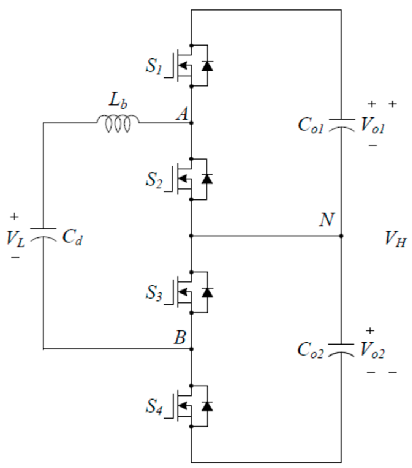
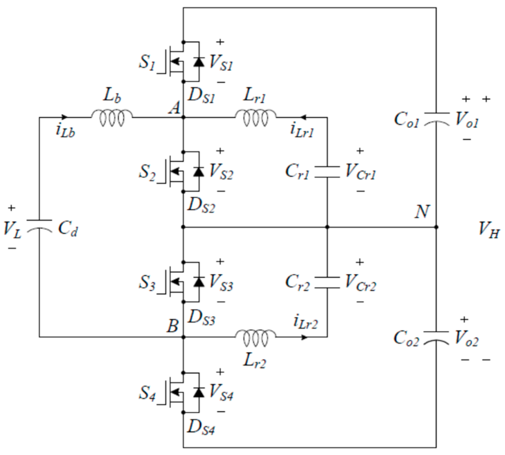
2.1. Circuit Configuration

Figure 2 shows the circuit diagram of the proposed converter. VL is the low voltage. VH is the high voltage. Cd, Lb, S1, S2, S3, S4, Co1, and Co2 consist of the bidirectional three-level DC–DC converter. Power switches (S1 ~ S4) include the body diodes (DS1 ~ DS4), respectively. Two identical LC circuits (Lr1 = Lr2 = Lr, Cr1 = Cr2 = Cr) are used for removing the turn-on switching losses of power switches. Power switches operate at a constant switching period Ts. The on-time of S1 (S2) is the same as the on-time of S4 (S3). The on-time of S1 (S2) is shifted by Ts/2 with respect to the on-time of S4 (S3). S1 (S3) and S2 (S4) operate complementary with a small dead time Td. The inductor Lb is large enough so that the inductor current iLb is continuous. The capacitors Cd, Co1, and Co2 are large enough so that the capacitor voltages VL, Vo1, and Vo2 are constant. It is assumed that Vo1 + Vo2 = VH and Vo1 = Vo2 = VH/2. The resonant frequency fr of the LC resonant circuit is assumed to be lower than the switching frequency fs of the converter. The capacitor voltages VCr1 and VCr2 are supposed to be constant during Ts.

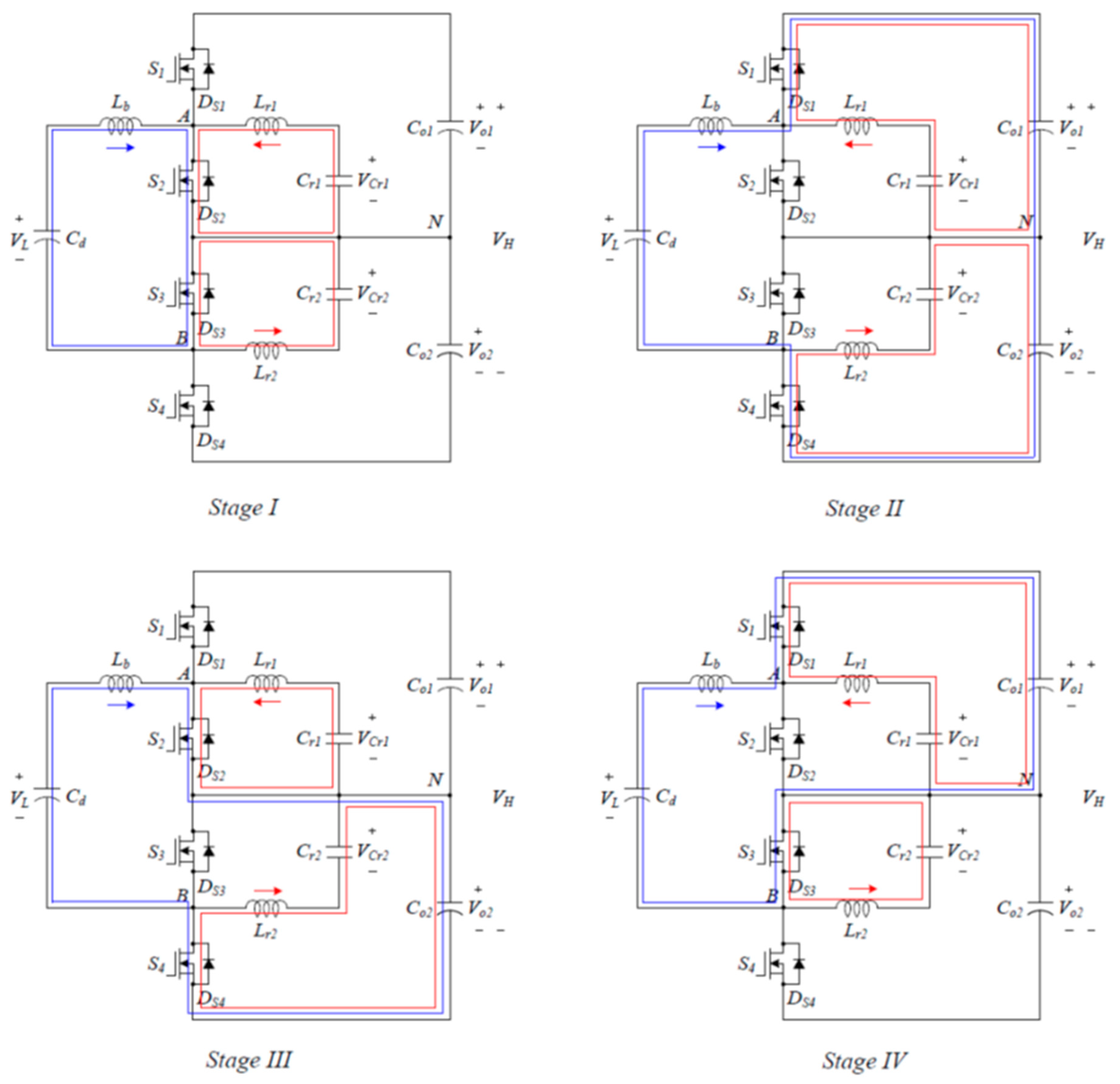
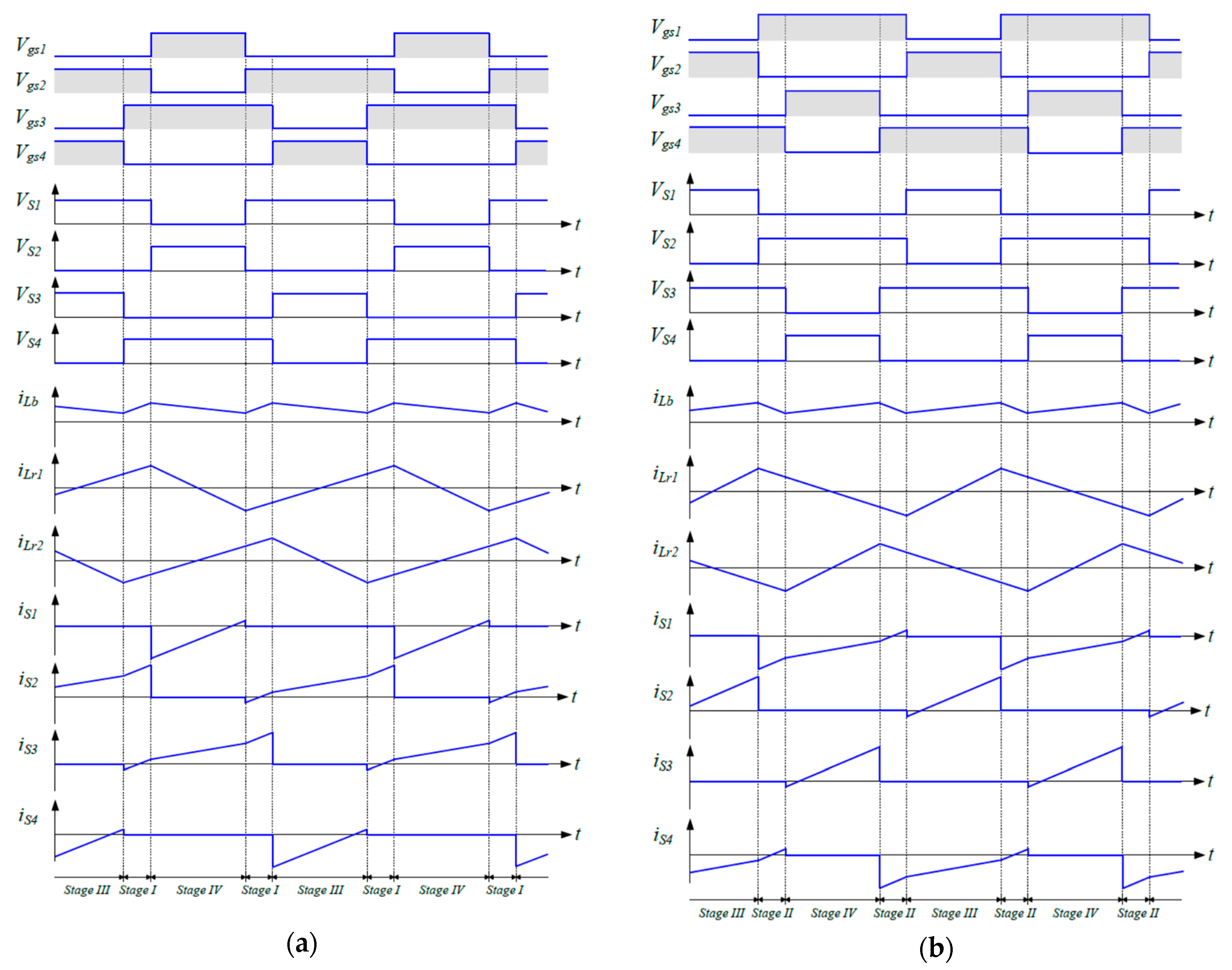
2.2. Control Operation

The proposed converter operates in a step-up mode when the electric power is transferred from VL to VH. As S2 and S3 are the main control switches, the duty cycle D is defined as the ratio between the on-time Ton of S2 (S3) and Ts. The proposed converter operates in a step-down mode when the electric power is transferred from VH to VL. S1 and S4 are the main control switches in the step-down mode. The duty cycle D is defined as the ratio between the on-time of S1 (S4) and Ts. Only the operation principles of the converter in the step-up mode are addressed here because the operation principles of the converter in both modes are analogous. Figure 3 shows the circuit diagrams of the proposed converter according to the switches’ states in the step-up mode. The proposed converter has four operation stages:
Stage I: The converter is in Stage I only when D > 0.5. S2 and S3 are turned on. S1 and S4 are turned off. iLb flows through Lb, S2, S3, and Cd. The following equation is obtained as
V L + L b d i L b d t = 0 .
iLr1 flows through Lr1, S2, and Cr1. The resonance between Lr1 and Cr1 is expressed as
V C r 1 + L r 1 d i L r 1 d t = 0 ,
C r 1 d V C r 1 d t = i L r 1 .
iLr2 flows through Lr2, Cr2, and S3. The resonance between Lr2 and Cr2 is expressed as
V C r 2 + L r 2 d i L r 2 d t = 0 ,
C r 2 d V C r 2 d t = i L r 2 .
S2 conducts iLb and iLr1, while S3 conducts iLb and iLr2.
Stage II: The converter is in Stage II only when D < 0.5. S2 and S3 are turned off. S1 and S4 are turned on. iLb flows through Lb, S1, Co1, Co2, S4, and Cd. The following equation is obtained as
V H + L b d i L b d t V L = 0 .
iLr1 flows through Lr1, S1, Co1, and Cr1. The resonance between Lr1 and Cr1 is expressed as
V C r 1 + L r 1 d i L r 1 d t + V o 1 = 0 ,
C r 1 d V C r 1 d t = i L r 1 .
iLr2 flows through Lr2, Cr2, Co2, and S4. The resonance between Lr2 and Cr2 is expressed as
V C r 2 + L r 2 d i L r 2 d t + V o 2 = 0 ,
C r 2 d V C r 2 d t = i L r 2 .
S1 conducts iLb and iLr1, while S4 conducts iLb and iLr2.
Stage III: S2 and S4 are turned on. S1 and S3 are turned off. iLb flows through Lb, S2, Co2, S4, and Cd. The following equation is obtained as
V o 2 + L b d i L b d t V L = 0 .
iLr1 flows through Lr1, S2, and Cr1 in a similar way to Stage I. iLr2 flows through Lr2, Cr2, Co2, and S4 in a similar way to Stage II. S2 conducts iLb and iLr1, while S4 conducts iLb and iLr2.
Stage IV: S1 and S3 are turned on. S2 and S4 are turned off. iLb flows through Lb, S1, Co1, S3, and Cd. The following equation is obtained as
V o 1 + L b d i L b d t V L = 0 .
iLr1 flows through Lr1, S1, Co1, and Cr1 in a similar way to Stage II. iLr2 flows through Lr2, Cr2, and S3 in a similar way to Stage I. S1 conducts iLb and iLr1, while S3 conducts iLb and iLr2.
Figure 4 shows the operation waveforms of the converter in the step-up mode, for D > 0.5 and D < 0.5, respectively. Vgs1, Vgs2, Vgs3, and Vgs4 are the gate signals for S1 ~ S4, respectively. iS1, iS2, iS3, and iS4 are the switch currents for S1 ~ S4, respectively.

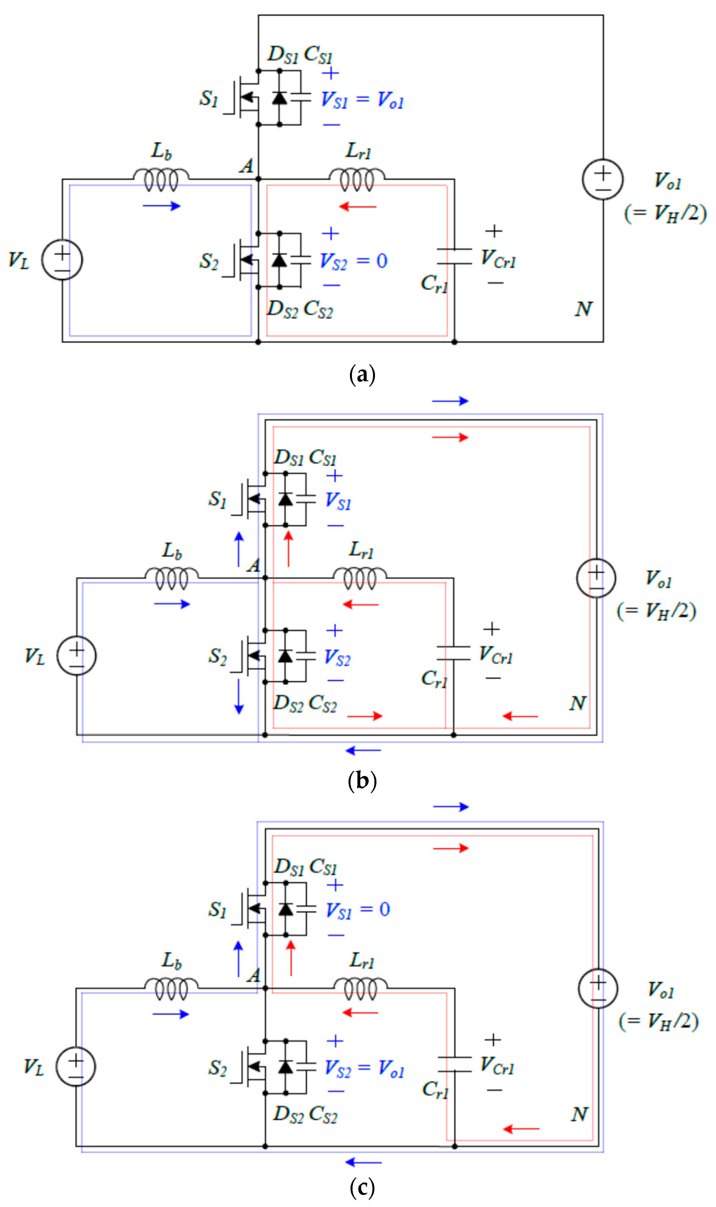
2.3. Soft-Switching Condition

Figure 5 shows the equivalent circuit diagrams of the proposed converter for the turn-on switching transition for S1. This switching transition period corresponds to the switching time from Stage I to Stage IV in the step-up mode. CS1 and CS2 are the parasitic output capacitances of S1 and S2, respectively. As shown in Figure 5a, CS1 has been charged to Vo1 as iLb and iLr1 flow through S2. Figure 5b shows the circuit diagram for the switching transition moment when S2 is turned off. iLb and iLr1 are split up between the capacitances, charging CS2 and discharging CS1. CS1 is completely discharged by iLb and iLr1, which flows in reverse through S1. The switch voltage VS1 becomes zero before S1 is turned on. S1 can be turned on at zero voltage when a gating signal is applied to S1, as shown in Figure 5c. CS2 has been charged to Vo1 as iLb and iLr1 flow through S1. The switching transition for other power switches is analogous to the switching transition for S1.
The switch current iS becomes the sum of two inductor currents as iLb + iLr1 for S1 and S2 and iLb + iLr2 for S3 and S4, respectively. In order to achieve the zero-voltage switching, iS should flow in reverse through the body diode of the switch at the switching transition moment. Then, iS should be lower than the zero current at the switching transition moment. For the moment from Stage I to Stage IV, the zero-voltage switching condition for S1 can be expressed as
| i L b , a v g | + Δ i L b 2 + Δ i L r 1 2 > 0
where ∆iLb and ∆iLr1 are
Δ i L b = V L L b D T s ,
Δ i L r 1 = V L L r 1 D T s .
iLb is the current ripple of Lb, and ∆iLr1 is the current ripple of Lr1. ǀiLb,avgǀ is the absolute value of the average inductor current iLb,avg. By the assumption that Lr1 = Lr2 = Lr, the following relation can be obtained from Equation (13) as
P d V L + V L T o n 2 L b + V L T o n 2 L r > 0
where Pd is the rated power of the proposed converter. For the moment from Stage IV to Stage I, the zero-voltage switching condition for S2 can be expressed as
| i L b , a v g | Δ i L b 2 Δ i L r 2 < 0
which can be rewritten by Equations (14) and (15) as
P d V L V L T o n 2 L b V L T o n 2 L r < 0 .
Once Lr is determined by Equation (18), Equation (16) can be satisfied without any constraint. By simplifying Equation (18), the inductance of Lr can be chosen, which gives the design criterion of Lr as
L r < L b V L 2 T o n 2 P d L b V L 2 T o n .
On the other hand, the switch current should operate under the above-resonant continuous mode to ensure the zero-voltage switching operation. Therefore, the switching frequency fs (= 1/Ts) of the converter should be higher than the resonant frequency fr of the LC resonant circuit [22]. After the selection of Lr, the capacitance of Cr can be determined by the following condition as
f r = 1 2 π L r C r < f s .

3. Simulation and Experimental Results

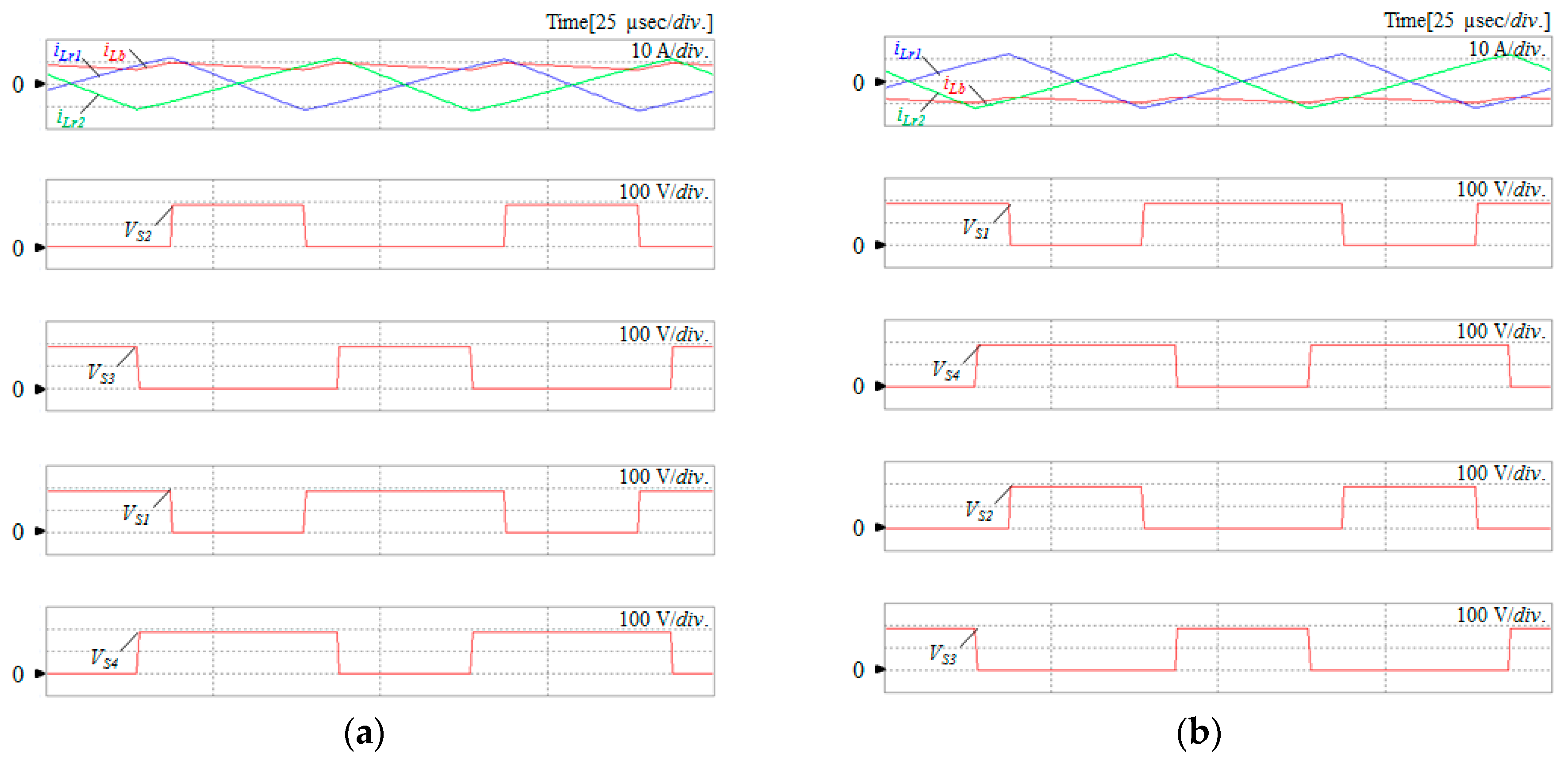
3.1. Simulation Results

Simulation results were obtained for the conventional converter in Figure 1 and the proposed converter in Figure 2. The simulations have been carried out by the physical security information management (PSIM) electronic simulation software. For the key system parameters of VL = 150 V, VH = 370 V, Pd = 1000 W, Ts = 50 μsec, Td = 2 μsec, Lb = 600 μH, and Co1 = Co2 = 560 μF, Figure 6 shows the simulation results for the conventional converter. Figure 6a shows the simulation results for the step-up mode, and Figure 6b shows the simulation results for the step-down mode. As shown in Figure 6, a voltage spike is observed at the moment that each switch is turned off. This voltage spike causes the turn-on switching loss for the power switch, which eventually decreases the power efficiency. On the other hand, Figure 7 shows the simulation results of the proposed converter. The resonant parameters, such as Lr = 100 μH and Cr = 2 μF, were used. Figure 7a shows the simulation results for the step-up mode, and Figure 7b shows the simulation results for the step-down mode. Compared to the simulation results in Figure 6, no voltage spike is observed at the moment that each switch is turned off in the simulation results in Figure 7. With the help of the auxiliary circuit, the proposed converter eliminated the turn-on switching losses.

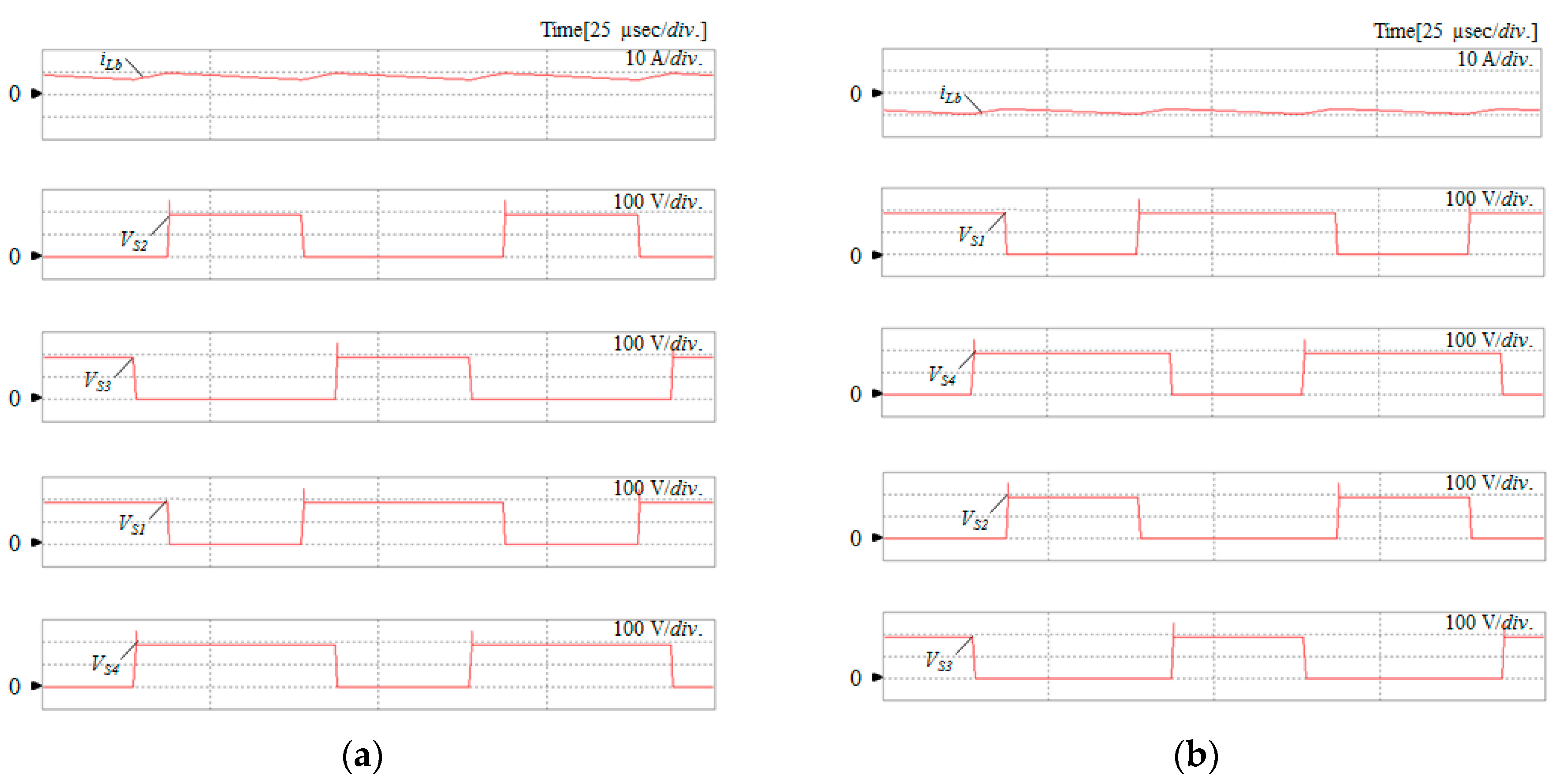
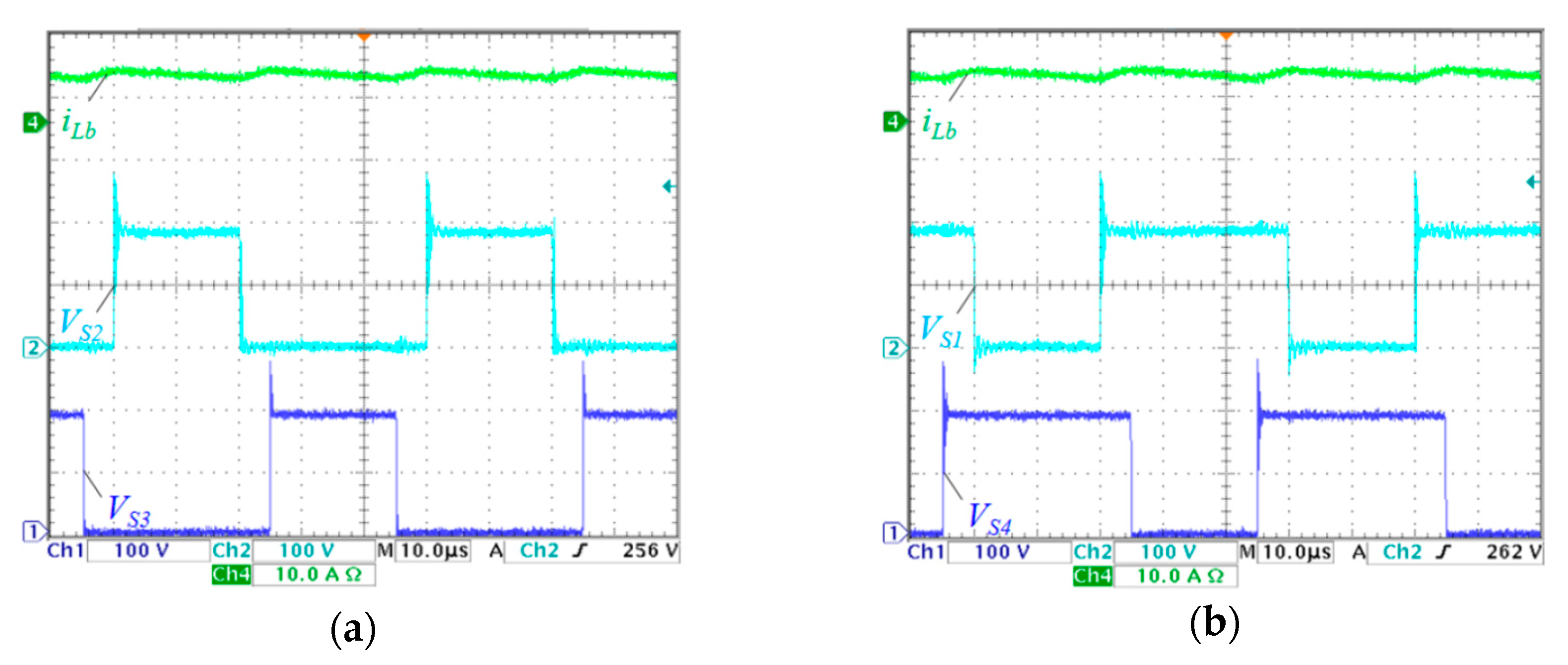
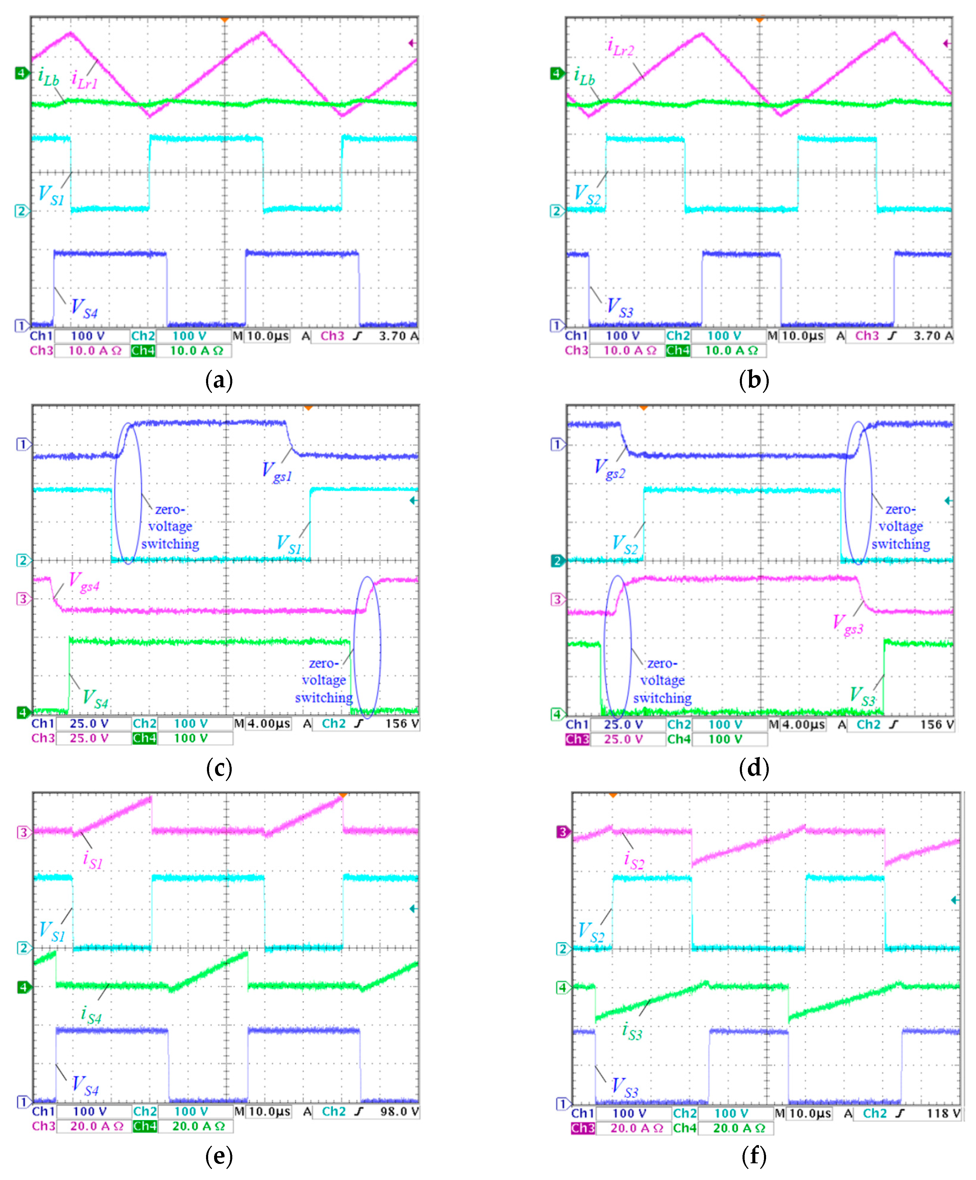
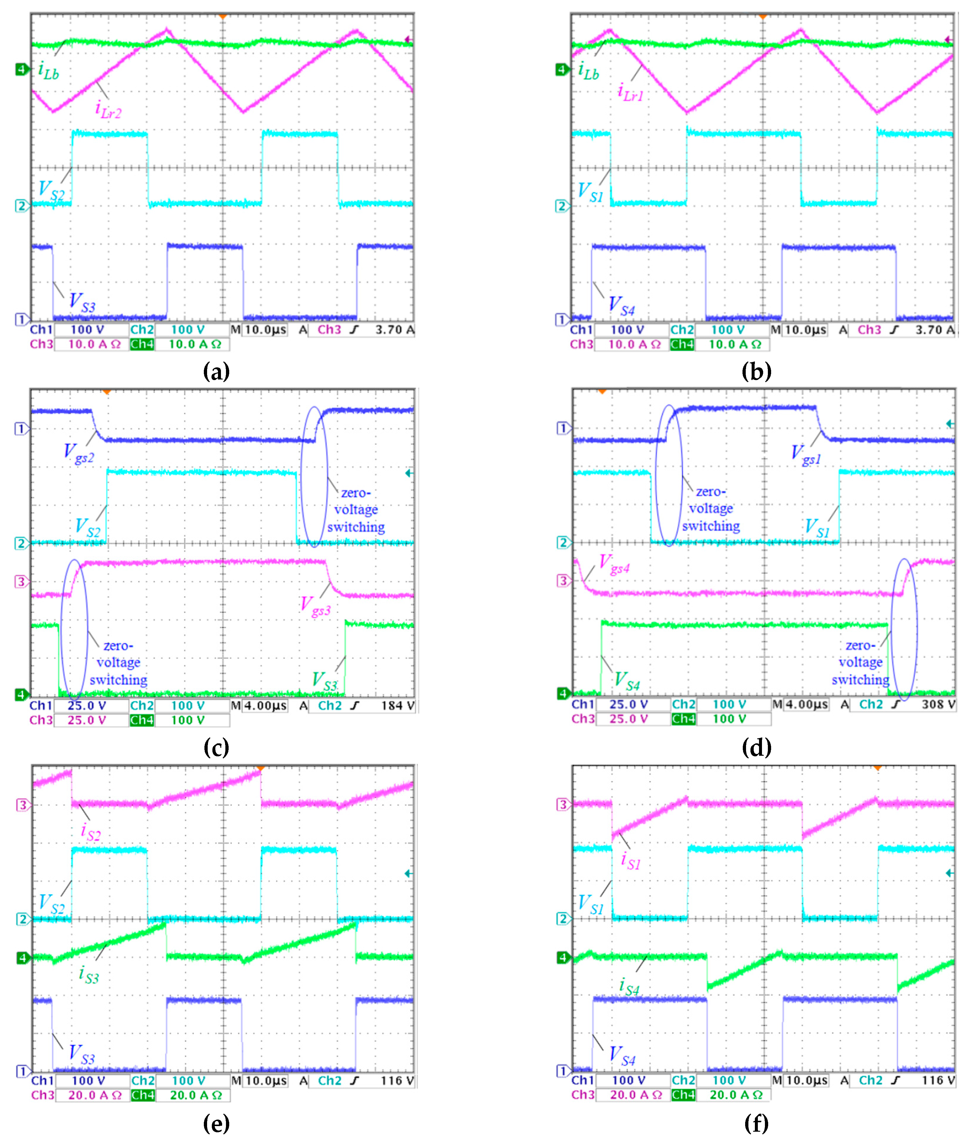
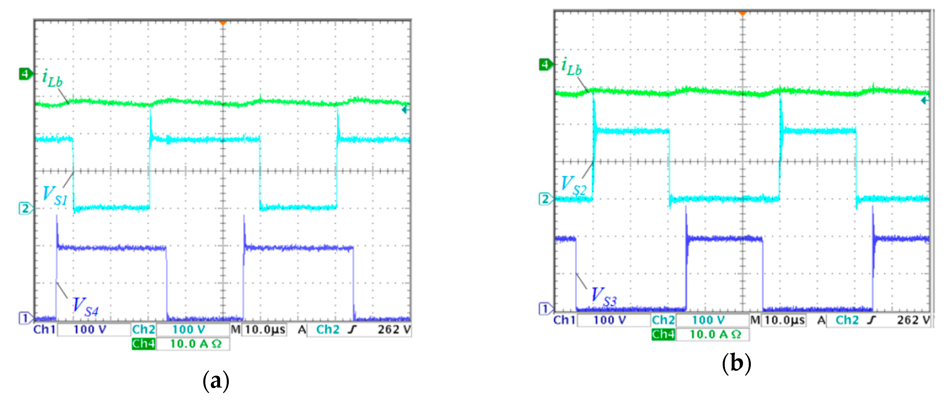
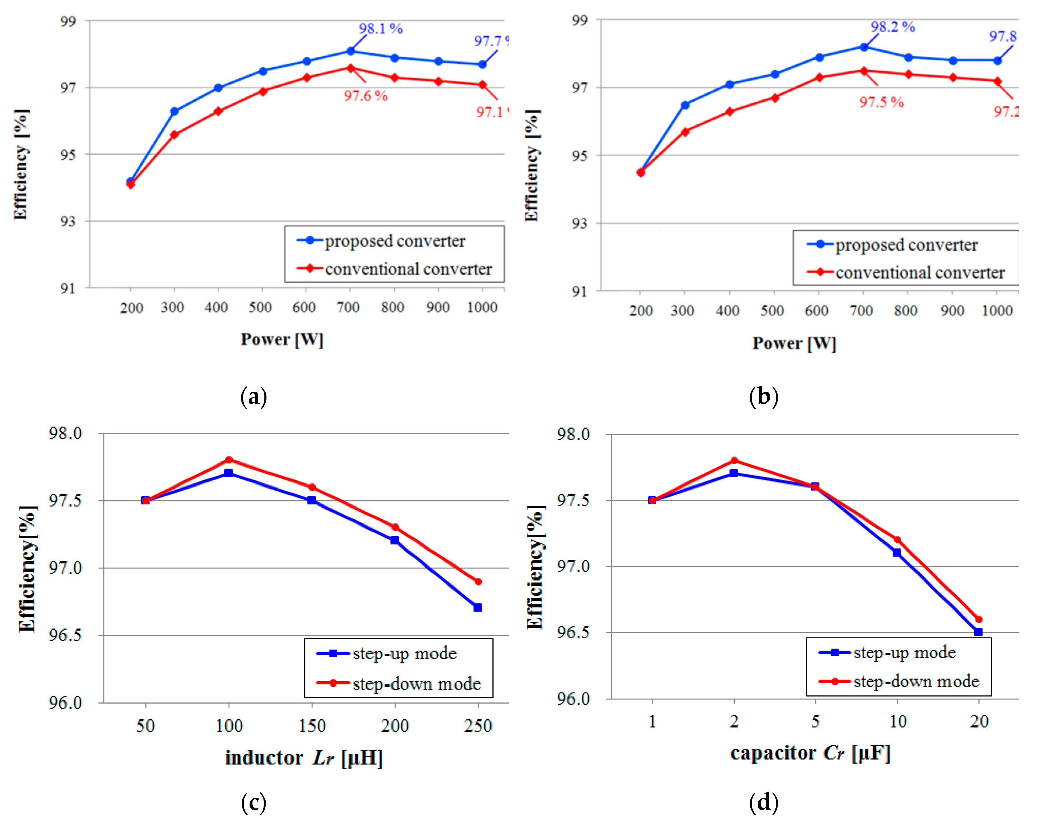
3.2. Experimental Results

A 1.0 kW prototype circuit was designed and tested for the electrical specifications and circuit parameters in Table 1. The low voltage VL ranges from 140 V to 160 V. The high voltage VH ranges from 360 V to 400 V. The valve-regulated lead–acid batteries were used for the low voltage side. Its nominal voltage for each battery cell is 24 V. This type of system configuration can be utilized for grid-tied battery energy storage system applications where the battery power can be transferred into the grid or recharged from the grid.
Figure 8 shows the experimental waveforms of the conventional converter in Figure 1 in the step-up mode. The conventional converter can be tested by removing the LC resonant circuits in the proposed converter. Figure 8a shows iLb, VS2, and VS3. Figure 8b shows iLb, VS1, and VS4. iLb is positively continuous because the converter is in the step-up mode. The on-time of S1 (S2) is shifted by Ts/2, with respect to the on-time of S4 (S3). As shown in Figure 8, a voltage spike is observed at the moment that each switch is turned off. This voltage spike causes the turn-on switching loss for the power switch, which eventually decreases the power efficiency. Figure 9 shows the experimental waveforms of the proposed converter in the step-up mode. Figure 9a shows iLb, iLr2, VS2, and VS3. Figure 9b shows iLb, iLr1, VS1, and VS4. iLb is positively continuous. iLr1 and iLr2 flow bidirectionally with a phase-shift of Ts/2 with respect to each other. At the moment that each switch is turned off, the voltage across the power switch is clamped to VH/2 as 185 V. Figure 9c shows Vgs2, VS2, Vgs3, and VS3. Figure 9d shows Vgs1, VS1, Vgs4, and VS4. As shown in Figure 9c,d, the switch voltage decreases to zero voltage before the gate signal is applied to the power switch. Power switches are turned on at zero voltage. Figure 9e shows iS2, VS2, iS3, and VS3. Figure 9f shows iS1, VS1, iS4, and VS4. Compared to the experimental results in Figure 8, no voltage spike is observed at the moment that each switch is turned off in Figure 9. With the help of the auxiliary circuit, the proposed converter has eliminated the turn-on switching losses for S1, S2, S3, and S4 effectively in the step-up mode.
Figure 10 shows the experimental waveforms of the conventional converter in the step-down mode. Figure 10a shows iLb, VS1, and VS4. Figure 10b shows iLb, VS2, and VS3. iLb is negatively continuous because the converter is in the step-down mode. The on-time of S1 (S2) is shifted by Ts/2, with respect to the on-time of S4 (S3). As shown in Figure 10, a voltage spike is observed at the moment that each switch is turned off. This voltage spike causes the turn-on switching loss for the power switch, which eventually decreases the power efficiency. Figure 11 shows the experimental waveforms of the proposed converter in the step-down mode. Figure 11a shows iLb, iLr1, VS1, and VS4. Figure 11b shows iLb, iLr2, VS2, and VS3. iLb is negatively continuous. iLr1 and iLr2 flow bidirectionally with a phase-shift of Ts/2 with respect to each other. At the moment that each switch is turned off, the voltage across the power switch is clamped to VH/2 as 185 V. Figure 11c shows Vgs1, VS1, Vgs4, and VS4. Figure 11d shows Vgs2, VS2, Vgs3, and VS3. As shown in Figure 11c,d, the switch voltage decreases to zero voltage before the gate signal is applied to the power switch. Power switches are turned on at zero voltage. Figure 11e shows iS1, VS1, iS4, and VS4. Figure 11f shows iS2, VS2, iS3, and VS3. Compared to the experimental results in Figure 10, no voltage spike is observed at the moment that each switch is turned off in Figure 11. By the operation of the auxiliary circuit, the proposed converter has eliminated the turn-on switching losses for S1, S2, S3, and S4 in the step-down mode. By eliminating the turn-on switching losses, the proposed converter increases the power efficiency for both step-up and step-down modes.
Figure 12 shows the power efficiency curves of the converters according to the operation modes. The power efficiency has been calculated by dividing the output power by the input power. The digital power meter (WT-230, YOKOGAWA) was used for the efficiency measurement. Figure 12a shows the power efficiency curves in the step-up mode. The conventional converter has an efficiency of 97.1% at 1.0 kW. The peak efficiency is 97.6% at 0.7 kW. The proposed converter has an efficiency of 97.7% at 1.0 kW. The peak efficiency is 98.1% at 0.7 kW. Figure 12b shows the power efficiency curves in the step-down mode. The conventional converter has an efficiency of 97.2% at 1.0 kW. The peak efficiency is 97.5% at 0.7 kW. The proposed converter has an efficiency of 97.8% at 1.0 kW. The peak efficiency is 98.2% at 0.7 kW. Figure 12c shows the power efficiency curves of the proposed converter for different inductor values of Lr at the rated power when Cr is 2 μF. Figure 12d shows the power efficiency curves of the proposed converter for different capacitor values of Cr at the rated power when Lr is 100 μH. As shown in Figure 12c,d, the proposed converter shows its best performance when Lr = 100 μH and Cr = 2 μF are chosen for the resonant parameters.

3.3. Power Loss Analysis

The proposed converter improves the power efficiency by eliminating the turn-on switching loss Pturn_on of the power switch, which is the most significant part of power losses when the MOSFETs are used. The proposed converter has turn-off switching losses and conduction losses. Assuming that ∆iLr = ∆iLr1 = ∆iLr2, the average turn-off switching loss Pturn_off is
P t u r n _ o f f = V H 4 T s ( | i L b , a v g | + Δ i L r 2 )   t t u r n _ o f f
where tturn_off is the turn-off moment time, including the current falling time and the voltage rising time of the switch, as described in [23]. The average conduction loss Pcond is
P c o n d = R d s ( o n ) D   ( | i L b , a v g | + Δ i L r 2 ) 2
where Rds(on) is the on-state resistance of the power switch. Other power losses Pothers for Lb and switch gate-driving circuits are hardly affected by the proposed scheme, except the power losses for Lr1 and Lr2. The power loss Pres_ind in the resonant inductor Lr includes the copper loss and the core loss. Table 2 shows the power loss distributions of the converters for the step-up mode and the step-down mode. As the power level increases, the sum of Pturn_on, Pturn_off, and Pcond in the conventional converter is higher than the sum of Pturn_off, Pcond, and Pres_ind in the proposed converter.

4. Conclusions

This paper has suggested a soft-switching bidirectional three-level DC–DC converter, which can effectively reduce the switching power losses with a simple auxiliary circuit. Two LC resonant circuits were used for reducing the turn-on switching power losses of main power switches. Power switches are turned on at zero voltage by the resonant operation of the LC resonant circuits. The proposed converter has reduced switching power losses and improves power efficiency, compared to the previous converters, which operate without any auxiliary circuits, suffering from high switching losses. The steady-state operation of the proposed converter was described. Its zero-voltage switching condition was analysed. A 1.0 kW prototype circuit was designed and tested for the experimental verifications of the proposed converter. The proposed converter achieved higher power efficiency than the conventional converter. It achieved the power efficiencies of 97.7% in the step-up mode and 97.8% in the step-down mode for the rated load condition.
The proposed converter can be utilized for a grid-tied battery energy storage system, which requires high power efficiency and high power density. Because of their three-level power conversion structure, high performance inverters, such as neutral point-clamped and three-level inverters, can be interfaced with the proposed converter. The proposed converter can be applied for the bidirectional DC–DC converter for both single-phase and three-phase grid-connected applications. The proposed converter is expected to be a good candidate for the interface between the battery and the grid-connected inverter to exchange electrical power with high efficiency and manage energy conversion.

Author Contributions

W.Y.C. managed the project, and mainly wrote the manuscript. M.K.Y. performed the experiments, analyzed the data, and edited the manuscript.

Funding

This research was supported by the National Research Foundation of Korea (NRF-2016R1D1A3B03932350).

Conflicts of Interest

The authors declare no potential conflict of interest.

References

  1. Lin, C.C.; Yang, L.S.; Wu, G.W. Study of a non-isolated bidirectional DC-DC converter. IET Power Electron. 2013, 6, 30–37. [Google Scholar] [CrossRef]
  2. Sulake, N.R.; Venkata, A.K.D.; Choppavarapu, S.B. FPGA implementation of a three-level boost converter-fed seven-level dc-link cascade H-bridge inverter for photovoltaic applications. Electronics 2018, 7, 282. [Google Scholar] [CrossRef]
  3. Kim, J.Y.; Kim, H.S.; Beak, J.W.; Jeong, D.K. Analysis of effective three-level neutral point clamped converter system for the bipolar LVDC distribution. Electronics 2019, 8, 691. [Google Scholar] [CrossRef]
  4. Han, S.H.; Kim, H.G.; Cha, H.; Chun, T.W. Bi-directional multi-level converter for an energy storage system. J. Power Electron. 2014, 14, 499–506. [Google Scholar] [CrossRef]
  5. Mirzaei, A.; Farzanehfard, H.; Adib, E.; Jusoh, A.; Salam, Z. A fully soft switched two quadrant bidirectional soft switching converter for ultra-capacitor interface circuits. J. Power Electron. 2011, 11, 1–9. [Google Scholar] [CrossRef]
  6. Tan, L.; Wu, B.; Yaramasu, V.; Rivera, S.; Guo, X. Effective voltage balance control for bipolar-dc-bus-fed EV charging station with three-level dc-dc fast charger. IEEE Trans. Ind. Electron. 2016, 63, 4031–4041. [Google Scholar] [CrossRef]
  7. Tan, L.; Zhu, N.; Wu, B. An integrated inductor for eliminating circulating current of parallel three-level dc-dc converter-based EV fast charger. IEEE Trans. Ind. Electron. 2016, 63, 1362–1371. [Google Scholar] [CrossRef]
  8. Choi, W.Y.; Yang, M.K. High-efficiency design and control of Zeta inverter for single-phase grid-connected applications. Energies 2019, 12, 974. [Google Scholar] [CrossRef]
  9. Lee, H.J.; Kim, Y.H. Analysis and design of a ZVT resonant boost converter using an auxiliary resonant circuit. Electronics 2019, 8, 466. [Google Scholar] [CrossRef]
  10. Li, J.; Horck, F.B.M.; Daniel, B.J.; Bergveld, H.J. A high-switching-frequency flyback converter in resonant mode. IEEE Trans. Power Electron. 2017, 32, 8582–8592. [Google Scholar] [CrossRef]
  11. Xie, X.; Li, J.; Peng, K.; Zhao, C.; Lu, Q. Study on the single-stage forward-flyback PFC converter with QR control. IEEE Trans. Power Electron. 2016, 31, 430–442. [Google Scholar] [CrossRef]
  12. Li, Y.C. A novel control scheme of quasi-resonant valley-switching for high-power-factor ac-to-dc LED drivers. IEEE Trans. Ind. Electron. 2015, 62, 4787–4794. [Google Scholar] [CrossRef]
  13. Park, J.P.; Moon, Y.J.; Jeong, M.G.; Kang, J.G.; Kim, S.H.; Gong, J.C.; Yoo, C.S. Quasi-resonant controller with adaptive switching frequency reduction scheme for flyback converter. IEEE Trans. Ind. Electron. 2016, 63, 3571–3581. [Google Scholar] [CrossRef]
  14. Sergio, B.M.; Joan, N.A. A multilevel active-clamped converter topology – operating principle. IEEE Trans. Ind. Electron. 2011, 58, 3868–3878. [Google Scholar]
  15. Choi, W.Y.; Yang, M.K.; Suh, Y.S. High-efficiency supercapacitor charger using an improved two-switch forward converter. J. Power Electron. 2014, 14, 1–10. [Google Scholar] [CrossRef]
  16. Poorali, B.; Jazi, H.M.; Adib, E. Single-core soft-switching high step-up three-level boost converter with active clamp. IET Power Electron. 2016, 9, 2692–2699. [Google Scholar] [CrossRef]
  17. Wang, J.; Li, R.T.; Chung, H.S. An investigation into the effects of the gate drive resistance on the losses of the MOSFET-snubber-diode configuration. IEEE Trans. Power Electron. 2012, 27, 2657–2672. [Google Scholar] [CrossRef]
  18. Rodrigues, J.P.; Mussa, S.A.; Heldwein, M.L.; Perin, A.J. Three-level ZVS active clamping PWM for the DC-DC buck converter. IEEE Trans. Power Electron. 2009, 24, 2249–2258. [Google Scholar] [CrossRef]
  19. Rodrigues, J.P.; Mussa, S.A.; Barbi, I.; Perin, A.J. Three-level zero-voltage switching pulse-width modulation DC-DC boost converter with active clamping. IET Power Electron. 2010, 3, 345–354. [Google Scholar] [CrossRef]
  20. Wang, B.; Yuan, Y.; Zhou, Y.; Sun, X. Buck/boost bidirectional converter TCM control without zero-crossing detection. In Proceedings of the IEEE International Power Electronics and Motion Control Conference (IPEMC, 2016), Hefei, China, 22–26 May 2016. [Google Scholar]
  21. Wang, Y.; Yang, J.; Zhang, B.; Jiang, X.; Kang, Z.; Ni, T.; Li, W. TCM controller design for three-level bidirectional soft-switching dc-dc converter. In Proceedings of the IEEE International Symposium on Industrial Electronics (ISIE, 2019), Vancouver, BC, Canada, 12–14 June 2019; pp. 996–1001. [Google Scholar]
  22. Ang, S.; Oliva, A. Power Switching Converters; CRC Press: Boca Raton, FL, USA, 2011; pp. 1–488. [Google Scholar]
  23. Mohan, N. Power Electronics: A First Course; John Wiley & Sons: Hoboken, NJ, USA, 2012. [Google Scholar]
Figure 1. Circuit diagram of the conventional converter.
Electronics 08 00983 g001
Figure 2. Circuit diagram of the proposed converter.
Electronics 08 00983 g002
Figure 3. The circuit diagram of the proposed converter according to the switches’ states in the step-up mode.
Electronics 08 00983 g003
Figure 4. The operation waveforms when the converter operates in the step-up mode: (a) D > 0.5; (b) D < 0.5.
Electronics 08 00983 g004
Figure 5. The equivalent circuit diagrams of the proposed converter for the turn-on switching transition for S1: (a) Stage I in the step-up mode; (b) switching transition from Stage I to Stage IV in the step-up mode; (c) Stage IV in the step-up mode.
Electronics 08 00983 g005
Figure 6. The simulation results of the conventional converter: (a) Step-up mode; (b) step-down mode.
Electronics 08 00983 g006
Figure 7. The simulation results of the proposed converter: (a) Step-up mode; (b) step-down mode.
Electronics 08 00983 g007
Figure 8. The experimental waveforms of the conventional converter in the step-up mode: (a) iLb, VS2, and VS3; (b) iLb, VS1, and VS4.
Electronics 08 00983 g008
Figure 9. The experimental waveforms of the proposed converter in the step-up mode: (a) iLb, iLr2, VS2, and VS3; (b) iLb, iLr1, VS1, and VS4; (c) Vgs2, VS2, Vgs3, and VS3; (d) Vgs1, VS1, Vgs4, and VS4; (e) iS2, VS2, iS3, and VS3; (f) iS1, VS1, iS4, and VS4.
Electronics 08 00983 g009
Figure 10. The experimental waveforms of the conventional converter in the step-down mode: (a) iLb, VS1, and VS4; (b) iLb, VS2, and VS3.
Electronics 08 00983 g010
Figure 11. The experimental waveforms of the proposed converter in the step-down mode: (a) iLb, iLr1, VS1, and VS4; (b) iLb, iLr2, VS2, and VS3; (c) Vgs1, VS1, Vgs4, and VS4; (d) Vgs2, VS2, Vgs3, and VS3; (e) iS1, VS1, iS4, and VS4; (f) iS2, VS2, iS3, and VS3.
Electronics 08 00983 g011
Figure 12. The power efficiency curves of the converters: (a) Power efficiency curves in the step-up mode; (b) Power efficiency curves in the step-down mode; (c) Power efficiency curves for different inductor values of Lr at the rated power; (d) Power efficiency curves for different capacitor values of Cr at the rated power.
Electronics 08 00983 g012
Table 1. Electrical specifications and circuit parameters.
SymbolQuantityValue
VLlow voltage140–160 V
VHhigh voltage360–400 V
Pdrated power1000 W
Tsswiching period50 µsec
Tddead time2 µsec
S1, S2, S3, S4power switchIXFP30N25X3
CS1, CS2, CS3, CS4capacitor1450 pF
Lbinductor600 μH (CM508125)
Co1, Co2capacitor560 μF/450 V
Lr1, Lr2inductor100 μH (EE2828)
Cr1, Cr2capacitor2 μF/630 V
Table 2. Power loss distributions of the converters.
Step-Up ModeStep-Down Mode
Conventional ConverterProposed ConverterConventional ConverterProposed Converter
Pturn_on11.0 W0 W10.4 W0 W
Pturn_off7.6 W9.6 W7.4 W9.2 W
Pcond7.4 W9.0 W7.2 W8.6 W
Pres_ind0 W1.4 W0 W1.2 W
Pothers3.0 W3.0 W3.0 W3.0 W
Ptotal29.0 W23.0 W28.0 W22.0 W

