Article

Effect of Annealing Ambient on SnO2 Thin Film Transistors Fabricated via An Ethanol-based Sol-gel Route

1
School of Electronics Engineering, Kyungpook National University, Daegu 41566, Korea
2
Department of Electronic and Electrical Convergence Engineering, Hongik University, Sejong 30016, Korea
*
Authors to whom correspondence should be addressed.
Electronics 2019, 8(9), 955; https://doi.org/10.3390/electronics8090955
Submission received: 5 August 2019 / Revised: 27 August 2019 / Accepted: 27 August 2019 / Published: 29 August 2019
(This article belongs to the Special Issue Applications of Thin Films in Microelectronics)

Abstract

:
The effect of annealing ambient on SnO2 thin-film transistors (TFTs) fabricated via an ethanol-based sol-gel route was investigated. The annealing ambient has a significant effect on the structural characteristics and chemical composition and, in turn, the device performance. Although the crystalline-grain size of the SnO2 films annealed in air was the smallest, this size yielded the highest field-effect mobility. Compared with the minimization of boundary scattering via crystalline-size increase, augmentation of the free carrier concentration played a more critical role in the realization of high-performance devices. The fabricated SnO2 TFTs delivered a field-effect mobility, subthreshold swing, and on/off current ratio of 10.87 cm2/Vs, 0.87 V/decade, and 107, respectively.

1. Introduction

Oxide semiconductor-based thin-film transistors (TFTs) are characterized by high electron mobility, a wide band gap, and applicability to various high-performance and transparent devices. The demand for these TFTs has increased. Applications requiring TFTs include see-through displays, transparent sensors, and electrochromic windows [1,2,3,4]. Oxide semiconductor-based TFTs are expected to supersede the conventional Si-based TFTs. Therefore, oxide TFTs based on Indium-based metal oxides have been extensively studied in the last decade. However, indium is a costly and rare metal that is found in only a few mining spots worldwide [5] and, hence, a new metal oxide system (without rare metals such as indium) is required. Representative n-type metal oxide semiconductors include ZnO, In2O3, and SnO2. Among these materials, SnO2 has the largest band gap, and is characterized by a high intrinsic mobility and low melting point. These features are attractive for applications that require high performance and transparent materials [6,7,8]. Various deposition techniques can be used to fabricate metal oxide films [9,10,11]. Unfortunately, these fabrication techniques require complex equipment and result in high manufacturing costs. Alternative techniques, such as solution processing, are therefore necessary. In particular, the solution processing-based fabrication of oxide TFTs is simple, low cost, and compatible with spin coating and inkjet printing [12,13,14]. A sol-gel process, i.e., one of the representative solution processes, is simple, easily controlled, and represents a cost-effective method of forming metal-oxide films. The quality of the final-formed film can be strongly influenced by precursors, substrate types, annealing temperature, and annealing conditions.
The present investigation was aimed at elucidating the effect of annealing ambient on the electrical performance of SnO2 TFTs fabricated by means of a sol-gel method. Annealing conditions play a critical role in determining the defect sites formed inside the material and, hence, have a significant influence on the device performance [15,16,17].

2. Materials and Methods

Tin (II) chloride dihydrate (SnCl2·2H2O, 0.001 mol) purchased from Sigma Aldrich (St. Louis, MO, USA) and was used as the precursor. The SnCl2 precursor was dissolved in 20 mL ethanol, thereby yielding a 0.050 M solution. SnO2 thin films were obtained by spin-coating (3000 rpm, 50 s) the Si/SiO2 substrate, which was previously cleaned during a 60-min ultraviolet/ozone (UV/O3) treatment. The fabricated films were dried in air for 10 min on a hot plate at 150 °C. Afterwards, the annealing process (heating for 4 h at 600 °C in a tube furnace) was executed under three different ambient conditions (air, vacuum, N2). The N2 gas flow into the furnace was maintained at a rate of 2.5 L/min, and the pressure inside the furnace was kept below 0.1 MPa under vacuum conditions. The SnO2 TFTs were fabricated on thermally grown 100-nm-thick SiO2/Si substrates. Moreover, 50-nm-thick Au electrodes were deposited as the bottom source and drain electrodes (channel width: 1000 µm, channel length: 100 µm) by using an e-beam evaporator and a lift-off process. The phase and structural characteristics of the films were determined via Grazing Incidence X-ray Diffraction (GIXRD, incident angle: 0.3°) with CuKα radiation (wavelength: 1.54 Å). The elemental composition and chemical state of the annealed films were evaluated by means of X-ray photoelectron spectroscopy (XPS; Quantera SXM (Physical Electronics, Chanhassen, MN, USA), chamber pressure 4 × 10⁻⁷ Pa). The optical properties were obtained at wavelengths ranging from 350 nm to 950 nm, using a LAMBDA 265 UV/Vis spectrophotometer. The surface morphology of the films was examined via scanning probe microscopy (SPM; Park NX20 (Park Systems, Suwon, Korea), tapping mode). In addition, the electrical properties of the TFTs were measured in air using a Keithley 2636B semiconductor parameter(Keithley Instruments, Cleveland, OH, USA) analyzer and a probe station.

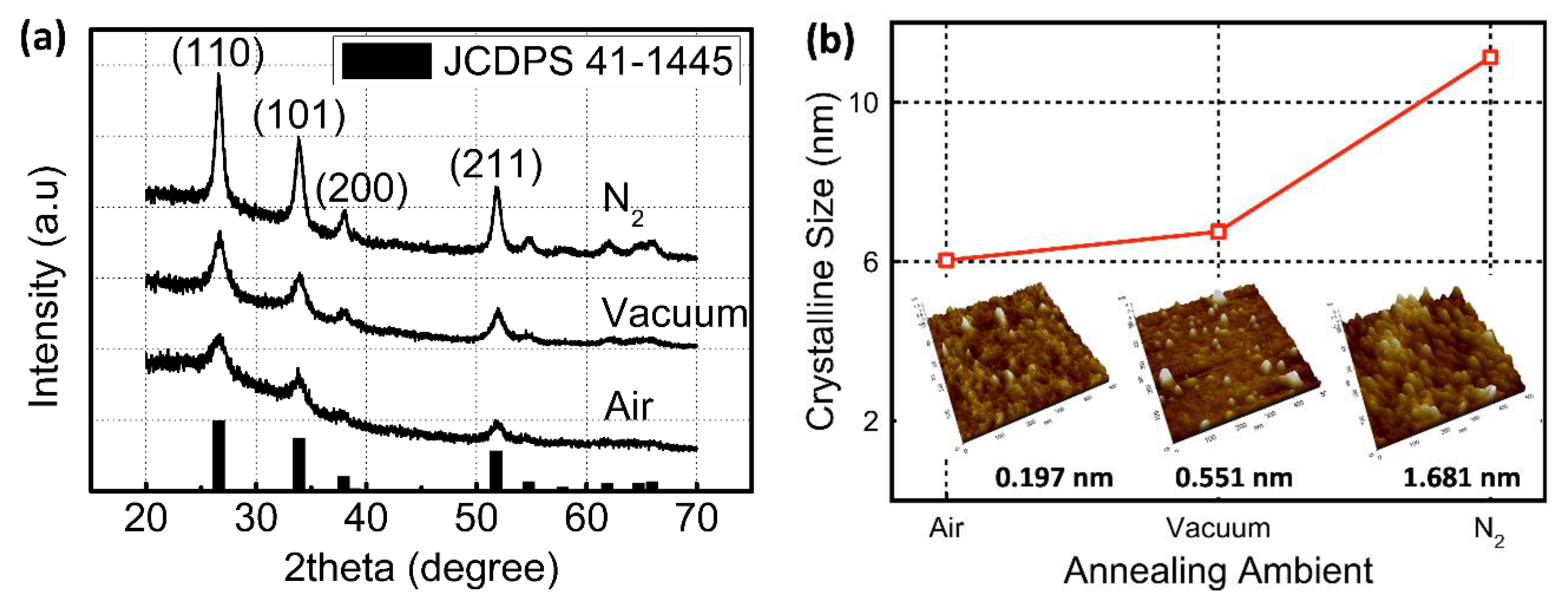
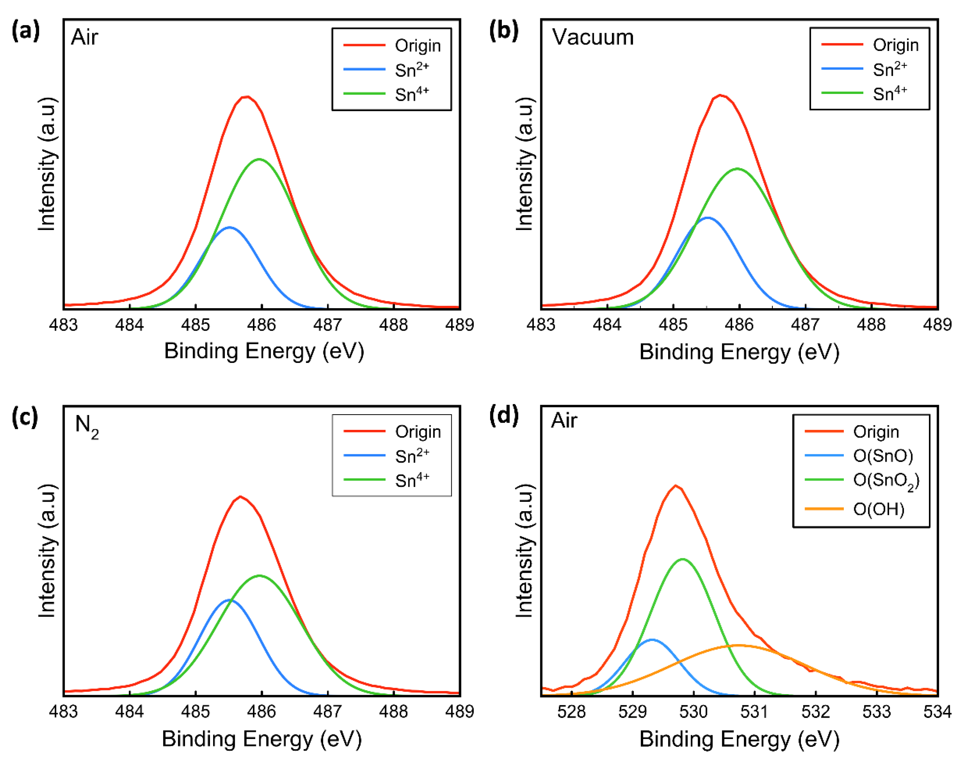
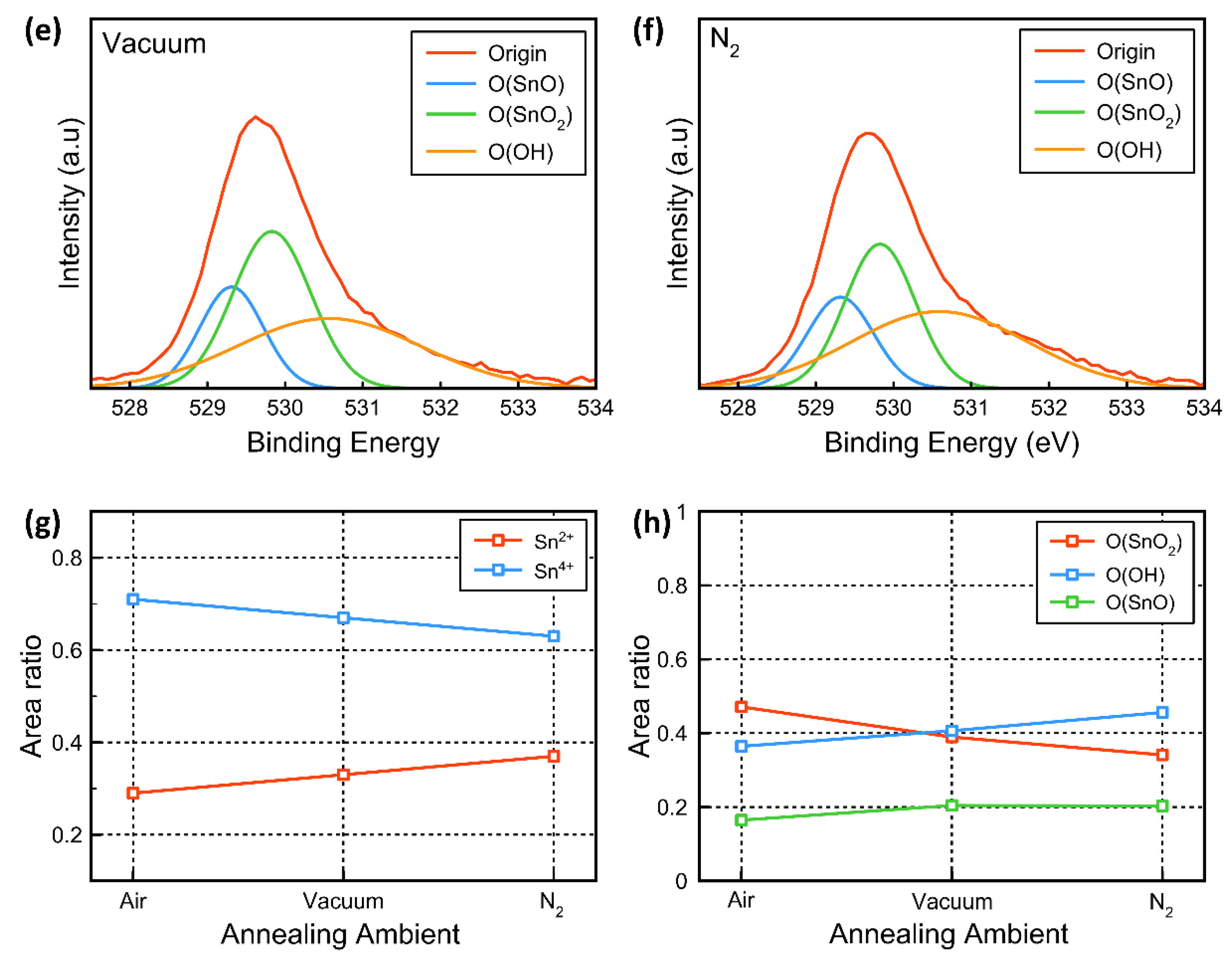
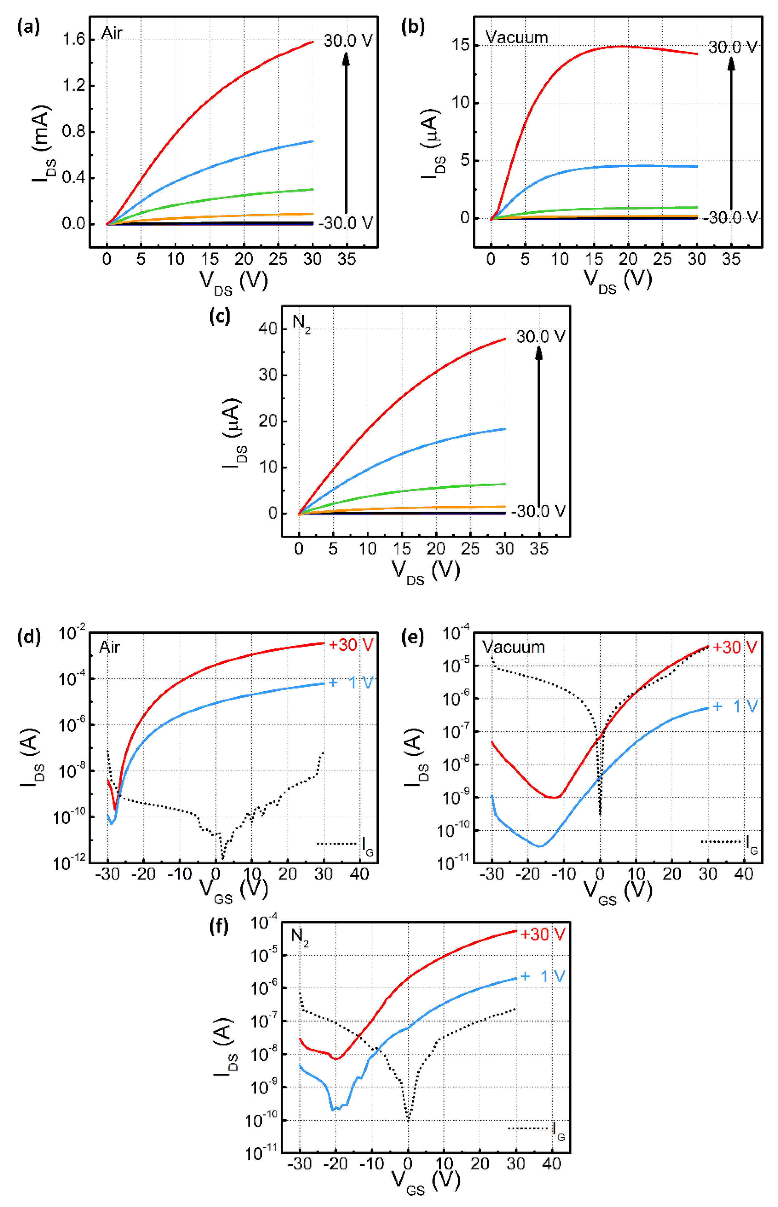
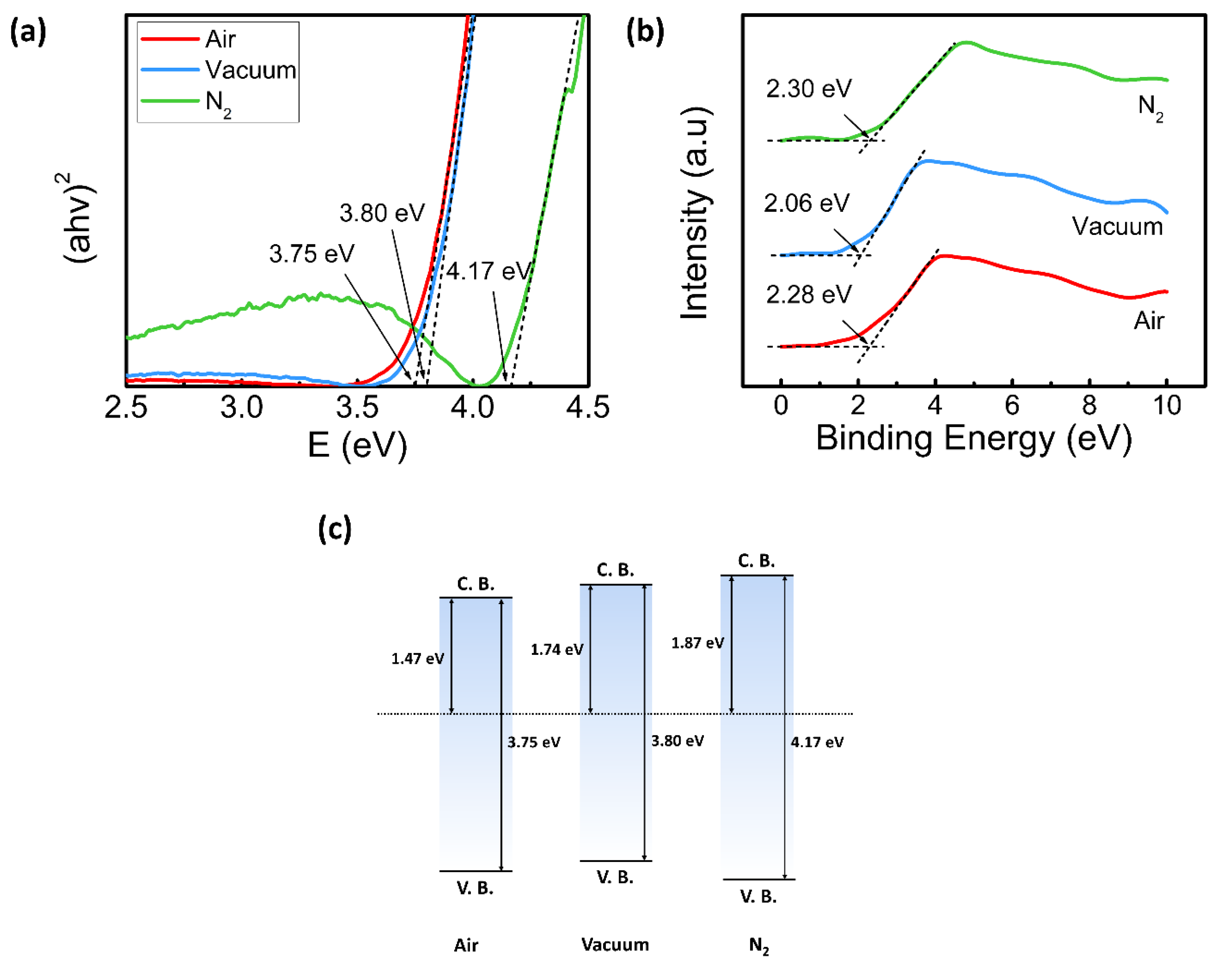
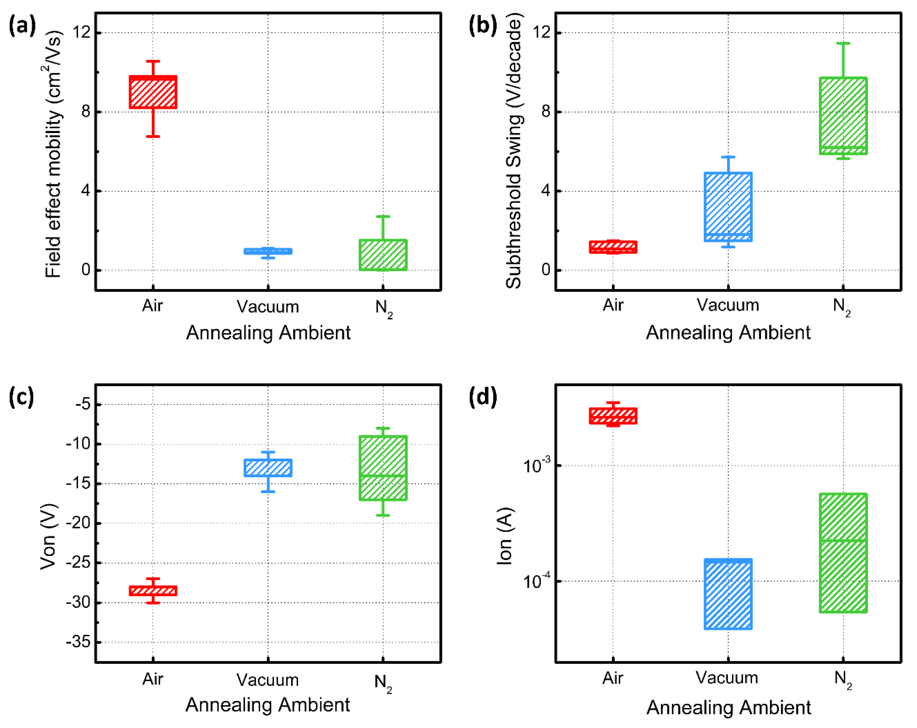
3. Results and Discussion

The prepared thin films were annealed at 600 °C for 4 h under three different ambient conditions: air, vacuum, and N2. The GIXRD spectra of the crystallized films, Figure 1a, correspond to the tetragonal phase of SnO2 (JCPDS 41-1445), i.e., polycrystalline tetragonal SnO2 occurred in each annealed film. Diffraction peaks at 26.6°, 33.8°, 37.9°, and 51.7° correspond to the (110), (101), (200), and (211) crystal planes, respectively, of this phase. The strongest peak intensities were observed for the TFT annealed in N2. The full width at half-maximum (FWHM) of a given GIXRD peak is closely correlated with the crystallite size of a particular crystal orientation. The FWHM of the SnO2 (110) peak was narrower than those of the other peaks, suggesting that SnO2 crystallites grew initially in the (110) plane.
The crystalline size of the films (see Figure 1b) was calculated from the Scherrer equation, which is given as follows:
D = 0.9 λ β cos θ
where, D, λ, β, and θ denote the crystalline size, CuKα wavelength (1.54 Å), full width at half-maximum of the peak, and peak position, respectively. Measured β values of 0.0236, 0.0211, and 0.0128 yielded D values of 6.03, 6.74, and 11.13 nm for the (110) phase of the SnO2 thin films annealed in air, vacuum, and N2, respectively. As the SPM images and root mean square (RMS) values of the films show (see inset of Figure 1b), the crystalline-grain size of the film annealed in N2 is significantly larger than that of the films annealed in vacuum and air.
The chemical composition of films annealed under different ambient conditions was determined via by XPS. The Sn composition was determined from the Sn 3d5/2 spectra (see Figure 2). The Sn 3d5/2 spectrum consists of two peaks, which occur at 485.51 and 485.96 eV and correspond to Sn2+ and Sn4+, respectively. The O 1s peak is split into three peaks associated with SnO (Sn2+), SnO2 (Sn4+), and hydroxide (OH groups) at 529.3, 530, and 530.9 eV, respectively. The Sn4+/Sn2+ ratio of the films annealed in air is considerably higher than those of the films annealed under other conditions. Compared with the amounts converted under other conditions, more SnO is converted into SnO2 during annealing in air.
Figure 3 shows the electrical characteristics of thin-film transistors (TFTs) fabricated under different annealing ambient conditions (i.e., air, vacuum, and N2). The fabricated devices have a bottom gate and bottom source/drain structure. The gate is p+ heavily doped Si and the gate dielectric is thermally grown SiO2. Furthermore, the source/drain electrodes are composed of Au. Figure 3a–c shows the output (IDS-VDS) characteristics of the fabricated SnO2 TFTs exposed to the different annealing ambient conditions. The IDS-VDS curves are probed at gate voltages of −30, −20, −10, 0, 10, 20, and 30 V. In the low VDS region of the curves, IDS changes non-linearly with VDS. This resulted from the relatively high work function of Au, compared with that of SnO2, and the consequent Schottky contact between the SnO2 channel and the Au source/drain electrodes [18,19,20]. The negative output differential resistance effect observed in Figure 3b was induced by the large gate leakage current. Figure 3d–f presents the transfer (IDS-VGS) characteristics of the fabricated SnO2 TFTs exposed to different annealing ambient conditions and a biased drain voltage of +30.0 V and +1.0 V. The fabricated TFTs exhibited conventional n-type semiconductor properties with negative turn on voltage (Von) and a normal on state (depletion mode). This indicates that excessive free carriers occur in sufficient numbers in the fabricated SnO2 thin films, leading to easy formation of the channel at an applied gate voltage of +0.0 V. The performance of the fabricated SnO2 TFTs is evaluated via four representative parameters, i.e., the field-effect mobility, on-current, subthreshold swing, and turn on voltage (Von). The field-effect mobility in the saturation region can be calculated from the saturation current of the transistor:
I D S = μ C i W 2 L ( V G V t h ) 2
where, Ci, W, L, and Vth denote the gate oxide capacitance per unit area, width of the channel, length of the channel, and threshold voltage, respectively. The calculated field-effect mobility and on-current value are plotted in Figure 5. Mobility values of 10.87, 0.62, and 0.30 cm2/Vs, and on-current values of 3.5 × 10⁻³, 3.89 × 10⁻⁵, and 5.44 × 10⁻⁵ A were obtained for the TFTs annealed in air, vacuum, and N2, respectively.
The crystalline size of the active channel layer comprising TFTs plays a critical role in simultaneously improving the on-current and field-effect mobility via the suppression of boundary scattering [21]. This scattering decreases progressively with increasing crystalline size, thereby resulting in improved device performance. However, a different result was obtained in the present study. The smallest crystalline-grain size was calculated from the GIXRD data and SPM images of the SnO2 films annealed in air, but these films exhibited the highest field-effect mobility in the saturation regime (10.87 cm2/Vs). The effect of annealing condition on the device performance can be explained by determining the chemical composition of the SnO2 films. Furthermore, XPS analysis of the films revealed that the Sn4+/Sn2+ ratio of the films annealed in air is considerably larger than those of the films annealed under other conditions. Compared with that generated under other conditions, more SnO was converted into SnO2 during annealing in air. It is well known that there are two binary stoichiometric tin oxides, SnO and SnO2. SnO shows p-type semiconductor properties, and SnO2 show n-type semiconductor properties. In this system, according to the XPS data, the largest Sn4+/Sn2+ ratio was obtained for the films annealed in air. This means that the decrease in hole carriers generated in the p-type SnO semiconductor compensate less due to the increase in electron carriers generated in the n-type SnO2 semiconductor at the same time. The increase in the Sn4+/Sn2+ ratio indicated that the channel conductivity of the n-channel layer was enhanced and, consequently, the number of carriers increased. This results in strong n-type semiconductor properties with high electron carrier concentrations.
Figure 4 shows the energy level diagram determined from XPS and absorption spectra. The estimated bandgaps are 3.75, 3.80, and 4.17 eV, respectively. The conduction bandgap offset (ΔECB = Eg − ΔEVB) of the SnO2 films can be estimated from the XPS-measured valence band and absorption spectra. This value, which is strongly correlated with the carrier concentration [22], was lowest for the SnO2 films annealed in air, indicative of the high carrier concentration characterizing these films. The major carrier transport mechanism operating inside the metal oxide semiconductors, i.e., percolation conduction, is improved by filling the trap state at high carrier concentrations [23]. The improved field-effect mobility and on-current originated from a significant increase in the free carrier concentration, and the calculated mobility values concurred with the XPS results. Therefore, compared with the crystalline size, the chemical composition played a greater role in determining the field-effect mobility in the saturation region and the on-current of the fabricated SnO2 devices.
Moreover, the turn on voltage, and subthreshold swing (SS) were measured from the transfer characteristics and plotted in Figure 5b,c. Estimated voltage of −28.0, −11.0, −19.0 V, and SS values of 0.87, 5.73, 7.48 V/decade were obtained. The significant increase in the free carrier concentration of the SnO2 films annealed in air led to early turn on. Owing to the large number of free carriers, the channel was formed more easily in these TFTs than in the TFTs fabricated under other conditions. The interface trap concentration and bulk state trap, located at the semiconductor near the interface, concentration are inversely proportional to the SS value, and were lowest for the SnO2 films annealed in air [24]. For annealed SnO2 semiconductors, the trap site resulting from the formation of an OH group or crystal imperfection can be either shallow or deep level states lying in the forbidden bandgap [25]. An increase in the concentration of shallow trap sites (located at the band edge) resulted in degradation of the field-effect mobility and on-current. Similarly, an increase in the concentration of deep level trap sites (located close to the valence band) resulted in degradation of the SS. Therefore, the traps originating from the OH groups or crystal imperfection led to an increase in the concentration of both shallow and deep level trap states. The reduction in the on-current yielded on/off ratios of 107, 104, and 104 for the TFTs annealed in air, vacuum, and N2, respectively.

4. Conclusions

The effect of annealing ambient on SnO2 TFTs fabricated via an ethanol-based sol-gel route was investigated in this study. Annealing conditions have a significant effect on the structural characteristics and chemical composition and, in turn, the device performance. To achieve high-performance SnO2 TFTs, high Sn4+/Sn2+ ratios for enhancing the n-type semiconductor properties, and high Ovacancy/OH ratios for increasing the free carrier concentration and reducing the trap site concentration are required. The annealing process in air was helpful in meeting these requirements. The SnO2 films annealed in air had the smallest crystalline-grain size, but exhibited the highest field-effect mobility. Compared with the boundary-scattering minimization achieved by increasing the crystalline size of our system, the free carrier concentration played a more critical role in the realization of high-performance devices. The fabricated SnO2 TFTs delivered a field-effect mobility, SS, and on/off current ratio of 10.87 cm2/Vs, 0.87 V/decade, and 107, respectively.

Author Contributions

Conceptualization, W.–Y.L. and J.J.; Experiments and data analysis, H.L. and S.H.; Investigation, H.L., H.H., and K.K.; Writing—original draft preparation, S.H. and H.L.; Writing—Review & Editing, J.H.B., I.M.K., W.–Y.L., and J.J.

Funding

This work was supported by the Basic Science Research Program through the National Research Foundation of Korea (NRF) funded by the Ministry of Education (NRF-2016R1D1A3B03930896) and by the National Research Foundation of Korea (NRF) grant funded by the Korean government (MSIT) (2019R1F1A1059788).

Conflicts of Interest

The authors declare no conflict of interest.

References

  1. Nomura, K.; Ohta, H.; Takagi, A.; Kamiya, T.; Hirano, M.; Hosono, H. Room-temperature fabrication of transparent flexible thin-film transistors using amorphous oxide semiconductors. Nature 2004, 432, 488–492. [Google Scholar] [CrossRef] [PubMed]
  2. Yabuta, H.; Sano, M.; Abe, K.; Aiba, T.; Den, T.; Kumomi, H.; Nomura, K.; Kamiya, T.; Hosono, H. High-mobility thin-film transistor with amorphous InGaZnO4 channel fabricated by room temperature rf-magnetron sputtering. Appl. Phys. Lett. 2006, 89, 112123. [Google Scholar] [CrossRef]
  3. Tomai, S.; Nishimura, M.; Itose, M.; Matuura, M.; Kasami, M.; Matsuzaki, S.; Kawashima, H.; Utsuno, F.; Yano, K. High-Performance Thin Film Transistor with Amorphous In2O3–SnO2–ZnO Channel Layer. Jpn. J. Appl. Phys. 2012, 51, 3. [Google Scholar] [CrossRef]
  4. Ebata, K.; Tomai, S.; Tsuruma, Y.; Iitsuka, T.; Matsuzaki, S.; Yano, K. High-Mobility Thin-Film Transistors with Polycrystalline In–Ga–O Channel Fabricated by DC Magnetron Sputtering. Appl. Phys. Express 2012, 5, 011102. [Google Scholar] [CrossRef]
  5. Haxel, G.B.; Hedrick, J.B.; Orris, G.J. Rare earth elements: Critical resources for high technology, U.S. Geol. Surv. Fact Sheet 2002, 87, 2. [Google Scholar]
  6. Sun, J.; Lu, A.; Wang, L.; Hu, Y.; Wan, Q. High-mobility transparent thin-film transistors with an Sb-doped SnO2 nanocrystal channel fabricated at room temperature. Nanotechnology 2009, 20, 335204. [Google Scholar] [CrossRef]
  7. Ju, S.; Chen, P.; Zhou, C.; Ha, Y.-G.; Facchetti, A.; Marks, T.J.; Kim, S.K.; Mohammadi, S.; Janes, D.B. 1∕f noise of SnO2 nanowire transistors. Appl. Phys. Lett. 2008, 92, 243120. [Google Scholar] [CrossRef]
  8. Ellmer, K. Resistivity of polycrystalline zinc oxide films: Current status and physical limit. J. Phys. D Appl. Phys. 2001, 34, 3097–3108. [Google Scholar] [CrossRef]
  9. Fortunato, E.; Barquinha, P.; Pimentel, A.; Pereira, L.; Gonçalves, G.; Martins, R. Amorphous IZO TTFTs with saturation mobilities exceeding 100 cm2/Vs. Phys. Stat. Sol. (RRL) 2007, 1, R34–R36. [Google Scholar] [CrossRef]
  10. Dehuff, N.L.; Kettenring, E.S.; Hong, D.; Chiang, H.Q.; Wager, J.F.; Hoffman, R.L.; Park, C.-H.; Keszler, D. Transparent thin-film transistors with zinc indium oxide channel layer. J. Appl. Phys. 2005, 97, 64505. [Google Scholar] [CrossRef] [Green Version]
  11. Wang, L.; Yoon, M.-H.; Lu, G.; Yang, Y.; Facchetti, A.; Marks, T.J. High-performance transparent inorganic–organic hybrid thin-film n-type transistors. Nat. Mater. 2006, 5, 893–900. [Google Scholar] [CrossRef] [PubMed]
  12. Jang, J.; Kitsomboonloha, R.; Swisher, S.L.; Park, E.S.; Kang, H.; Subramanian, V. Transparent high-performance thin film transistors from solution-processed SnO2/ZrO2 gel-like precursors. Adv. Mater. 2013, 25, 1042–1047. [Google Scholar] [CrossRef] [PubMed]
  13. Pattanasattayavong, P.; Thomas, S.; Adamopoulos, G.; McLachlan, M.A.; Anthopoulos, T.D. p-channel thin-film transistors based on spraycoated Cu2O Films. Appl. Phys. Lett. 2013, 102, 163505. [Google Scholar] [CrossRef]
  14. Jang, J.; Kang, H.; Chakravarthula, H.C.N.; Subramanian, V. Fully inkjet-printed transparent oxide thin film transistors using a fugitive wettability switch. Adv. Electron. Mater. 2015, 1, 1500086. [Google Scholar] [CrossRef]
  15. Hwang, S.; Lee, J.H.; Woo, C.H.; Lee, J.Y.; Cho, H.K. Effect of annealing temperature on the electrical performances of solution-processed InGaZnO thin film transistors. Thin Solid Films 2011, 519, 5146–5149. [Google Scholar] [CrossRef]
  16. Sung, S.-Y.; Jo, K.-M.; Kim, S.-Y.; Lee, J.-H.; Kim, J.-J.; Heo, Y.-W. Effects of Post-Annealing Treatments on the Transfer Characteristics of Amorphous Indium-Gallium-Zinc Oxide Thin Film Transistors. J. Nanoelectron. Optoelectron. 2011, 6, 310–314. [Google Scholar] [CrossRef]
  17. D.M., P.; Mannam, R.; Rao, M.R.; Dasgupta, N.; Priyadarshini, D.; Ramanjaneyulu, M. Effect of annealing ambient on SnO2 thin film transistors. Appl. Surf. Sci. 2017, 418, 414–417. [Google Scholar]
  18. Yun, Y.; Choi, A.; Hahm, S.G.; Chung, J.W.; Lee, Y.U.; Jung, J.Y.; Kim, J.-Y.; Park, J.-I.; Lee, S.; Jang, J. Enhanced Performance of Thiophene-Rich Heteroacene, Dibenzothiopheno [6,5-b:6’,5’-f] Thieno[3,2-b]Thiophene Thin-Film Transistor With MoOx Hole Injection Layers. IEEE Electron Device Lett. 2017, 38, 649–652. [Google Scholar] [CrossRef]
  19. Jang, B.; Kim, T.; Lee, S.; Lee, W.-Y.; Kang, H.; Cho, C.S.; Jang, J. High performance ultrathin SnO2 thin film transistors by sol-gel method. IEEE Electron Device Lett. 2018, 39, 1179–1182. [Google Scholar] [CrossRef]
  20. Jang, B.; Kim, T.; Lee, S.; Lee, W.-Y.; Jang, J. Schottky Nature of Au/SnO2 Ultrathin Film Diode Prepared by Sol-gel Method. IEEE Electron Device Lett. 2018, 39, 1732–1735. [Google Scholar] [CrossRef]
  21. Gupta, N.; Tyagi, B.P. On-Current Modeling of Polycrystalline Silicon Thin-Film Transistors. Phys. Scr. 2005, 72, 339–342. [Google Scholar] [CrossRef]
  22. Ahn, B.D.; Lim, J.H.; Cho, M.-H.; Park, J.-S.; Chung, K.-B. Thin film transistor behavior and the associated physical origin of water annealed In-Ga-Zn oxide semiconductor. J. Phys. D Appl. Phys. 2012, 45, 445307-1–415307-6. [Google Scholar] [CrossRef]
  23. Kim, Y.-S.; Park, C.H. Rich Variety of Defects in ZnO via an Attractive Interaction between O Vacancies and Zn Interstitials: Origin of n -Type Doping. Phys. Rev. Lett. 2009, 102, 806403. [Google Scholar] [CrossRef] [PubMed]
  24. Choi, K.; Raza, S.R.A.; Lee, H.S.; Jeon, P.J.; Pezeshki, A.; Min, S.W.; Kim, J.S.; Yoon, W.; Ju, S.Y.; Lee, K.; et al. Trap density probing on top-gate MoS2 nanosheet field effect transistors by photo-exited charge collection spectroscopy. Nanoscale 2015, 7, 5617. [Google Scholar] [CrossRef] [PubMed]
  25. Chung, H.-J.; Mo, Y.-G.; Kim, H.D.; Park, J.-S.; Jeong, J.K. Electronic transport properties of amorphous indium-gallium-zinc oxide semiconductor upon exposure to water. Appl. Phys. Lett. 2008, 92, 72104. [Google Scholar]
Figure 1. (a) GIXRD patterns and (b) calculated crystalline sizes of the SnO2 films annealed in air, vacuum, and N2. The inset shows the SPM images.
Electronics 08 00955 g001
Figure 2. (a)–(c) Sn 3d5/2 XPS spectra and (d)–(f) O1s XPS spectra of SnO2 films annealed in air, vacuum, and N2. Sn 3d5/2 (g) and O 1s (h) compositions of films annealed in different annealing ambient conditions.
Electronics 08 00955 g002aElectronics 08 00955 g002b
Figure 3. ID-VD curves obtained for TFTs consisting of SnO2 films annealed in (a) air, (b) vacuum, and (c) N2. The corresponding transfer curves of SnO2 TFT annealed in (d) air, (e) vacuum, and (f) N2 with different VDS.
Electronics 08 00955 g003
Figure 4. (a) Dependence of (αhv)2 on the photon energy (hv) of SnO2 films annealed in air, vacuum, and N2. (b) XPS spectra collected from regions near the valence band. (c) Energy level diagram including the relative energy position of the Fermi level (EF) with respect to the conduction band minimum and valence band maximum.
Electronics 08 00955 g004
Figure 5. Extracted performance parameters of the fabricated SnO2 thin-film transistors: (a) field-effect mobility in the saturation regime, (b) SS, (c) Von, and (d) Ion.
Electronics 08 00955 g005

