Abstract
Y-doped SnO2 thin film transistors were successfully fabricated by means of sol-gel process. The effect of Y concentration on the structural, chemical, and electrical properties of sol-gel-processed SnO2 films was investigated via GIXRD, SPM, and XPS; the corresponding electrical transport properties of the film were also evaluated. The dopant, Y, can successfully control the free carrier concentration by suppressing the formation of oxygen vacancy inside SnO2 semiconductors due to its lower electronegativity and SEP. With an increase of Ywt%, it was observed that the crystallinity and oxygen vacancy concentration decreased, and the operation mode of SnO2 thin film transistor changed from accumulation (normally on) to enhancement mode (normally off) with a positive Vth shift.
1. Introduction
Metal-oxide semiconductors have received considerable attention as promising active channel materials for transistors for transparent displays and flexible and wearable optical and electronic devices due to their high mobility, high transparency, low cost, robust, CMOS process compatible stability, and good uniformity. Generally, n-type metal-oxide semiconductors, showing high mobility, have been used in these applications [1,2,3,4] (i.e., ZnO, In2O3, and SnO2). Among these, SnO2 has the highest mobility and the transparency due to its high intrinsic mobility and large bandgap [5]. In addition, SnO2 is inexpensive and shows good chemical and thermal stability at high temperatures [6]. It have been shown to be a candidate for application in gas sensors due to its high surface to volume ratio [7]. The melting point of this material makes crystallization easier than with other semiconductors. This relatively easy crystallization results in improved conductivity and mobility by suppressing grain boundary scattering [8]. In addition, SnO2 is a paradigmatic indium-free semiconductor. Indium, a costly, rare metal, is found in only a few mining sites worldwide [9]. However, the electronic configuration of Sn (1s22s2p63s2p6d105s2p2) is similar to that of In (1s22s2p63s2p6d104s2p6d105s2p1), and SnO2 semiconductor films are characterized by promising electrical properties [10,11,12,13,14]. Sol-gel processing represents a promising low cost fabrication method by which to obtain high-quality SnO2 films without using a conventional vacuum-based deposition process, requiring a complex and high cost vacuum system [15,16,17,18,19,20]. Unfortunately, oxygen vacancy inside metal oxide semiconductor leads to problems of stability and of the controllability of Vth. Therefore, controlling oxygen vacancy is critical to control the device performance. It is well known that the electronegativity and standard electrode potential (SEP) of the dopant can influence its carrier suppressed ability [21,22]. In this work, we choose yttrium as a dopant to suppress the carriers in the SnO2 semiconductor system, due to its lower electronegativity, SEP, and price. Y-doped SnO2 thin film transistors (TFTs) are therefore fabricated for the first-time. We use grazing incidence X-ray diffraction (GIXRD), scanning probe microscopy (SPM), and X-ray photoelectron spectroscopy (XPS) to investigate sol-gel-processed SnO2 films obtained with different Ywt%. To understand the effect of Ywt% on the electrical properties of the SnO2 films, we fabricate bottom gate TFTs on SiO2/Si substrates and evaluate the electrical properties at different Ywt% concentrations.
2. Materials and Methods
A simple inverted coplanar structure was adopted for SnO2 TFT fabrication. Heavily doped p-type Si and dry oxygen, thermally-grown, 100-nm-thick SiO2 layers were used as the bottom gate and insulator. The Au source/drain electrodes were formed by means of an e-beam evaporation and lift-off process. The designed channel width and length were 1000 µm and 100 µm, respectively. A SnCl2 sol-gel precursor (Sigma Aldrich, St. Louis, MO, USA) was prepared for the SnO2 films. A SnCl2 solution (concentration: 0.025 M) was prepared by dissolving tin (II) chloride dehydrate (SnCl2·2H2O, 0.25 mmol) in ethanol (10 mL). Then, 0.2, 0.5, and 1.0 wt% Y(NO3)2·4H2O was dissolved in the prepared SnCl2 solution. An UV/ozone process was conducted for 60 min to remove organic dust on the substrates. The prepared precursor solution was spin-coated at 3000 rpm for 50 s. After coating, the films were pre-annealed in air at 150 °C for 10 min to evaporate the solvent. To convert into SnO2, the films were annealed in a tube furnace at 500 °C for 2 h in air. The structural characteristics of films were investigated by a grazing incidence X-ray diffraction (GIXRD) (Philips X’pert Pro) with Cu Kα radiation (λ = 1.54 Å), where samples were irradiated at an angle of 0.3°. The surface morphology was examined using a scanning probe microscope (SPM: Park NX20, tapping mode). The chemical compositions of the films were investigated by X-ray photoelectron spectroscopy (XPS) (Quantera SXM), with a monochromatic Al Kα (1488 eV) source and a pass energy of 40 eV. The electrical properties of the TFTs were examined using a Keithley 2636B semiconductor parameter analyzer and a probe station in air.
3. Results and Discussion
Figure 1 shows the effect of Y3+ concentrations on the phase evolution of Y-doped SnO2 films annealed at 500 °C for 2 h. All the annealed Y-doped SnO2 films are poly-crystalline in nature. The GIXRD patterns revealed that all peaks were well matched with the standard tetragonal SnO2 pattern (JCPDS: 41-1445). The broaden diffraction peaks meant that the formed films were in the nanostructured phase. Diffraction peaks at 26.6°, 33.8°, 37.9°, and 51.7° corresponded to the (110), (101), (200), and (211) crystal planes of tetragonal SnO2, respectively. The full width at half-maximum (FWHM) of the obtained GIXRD peak was strongly correlated with the crystallite size of a particular crystal orientation. The FWHM of the SnO2 (110) peak was smaller than those of the other peaks, indicating that SnO2 crystallites grew initially in the (110) plane.
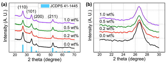
Figure 1.
(a) GIXRD patterns and (b) the GIXRD patterns near the (110) lattice plane with different Ywt%.
The average crystalline size of the annealed films was obtained using Scherrer’s formula (Equation (1)),
where D, λ, β, and θ denote the crystalline size, Cu Kα wavelength (1.54 Å), full width at half-maximum of the peak, and position of the peak, respectively. The obtained β values were 1.33, 1.26, 1.28, and 1.3, yielding D values of 6.13, 6.47, 6.37, and 6.27 nm for the (110) phase of formed pure SnO2 and Y-doped SnO2 semiconductor films. The microstrain and dislocation density were calculated using the relationship ε = βcosθ, and δ = 1/D2, respectively. The calculated values are listed in Table 1. Compared to pure SnO2 semiconductor films, there was a relative Bragg peak shift towards a smaller angle for Y-doped SnO2 semiconductor films. This Bragg peak position shift towards lower values in the of Y-doped SnO2 semiconductor films resulted from an increase in lattice parameter values, originating from the internal stress generated by the substitution of host Sn4+ (0.74 Å) ions by dopant Y3+ (1.04 Å) ions. In Y-doped SnO2 films, the peaks, corresponding to Y2O3, could not obtained. Y3+ ions cannot be segregated to form Y2O3, or the amount is too little to be detected (i.e., <1 wt%).

Table 1.
Crystalline size, microstain, and dislocation density of Y-doped SnO2 semiconductor films with different Ywt%.
The SPM images of the SnO2 semiconductor films with 0, 0.2, 0.5, and 1.0 wt% Y on SiO2/Si wafer annealed at 500 °C for 2 h are shown in Figure 2. The root mean square (RMS) values of the films obtained from SPM images are 0.97, 1.40, 2.45, and 2.74 nm for SnO2 semiconductor films with 0, 0.2, 0.5, and 1.0 wt% Y, respectively. The RMS values are increased with increased Ywt%. The surface roughness plays a critical factor to effect on device performance and the active channel layer with minimal surface roughness results in the better thin film transistor performance.
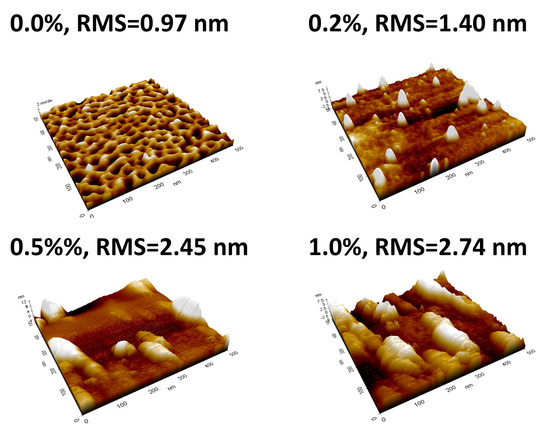
Figure 2.
SPM Images and RMS values, with different Ywt%.
The chemical composition of pure SnO2 and Y-doped SnO2 semiconductor films was investigated using XPS analysis. The Y-doped films showed XPS spectra, corresponding to Y located at 157.64 and 159.56 eV, and the spectra could be distinguished with two Gaussian Peaks of Y 3d5/2 and Y 3d3/2, indicating the formation of Y-O bonding in Figure 3a. The intensity of these spectra increased with increasing Ywt%. Figure 3b shows the XPS spectra of Sn 3d5/2 and Sn 3d3/2. Comparing to the binding energy of pure SnO2 films, the binding energy of the 0.5 wt% and 1.0 wt% Y-doped SnO2 films were shifted toward higher binding energy values. The binding energy shift towards high values could be associated with a phase transformation from SnO to SnO2 [23].
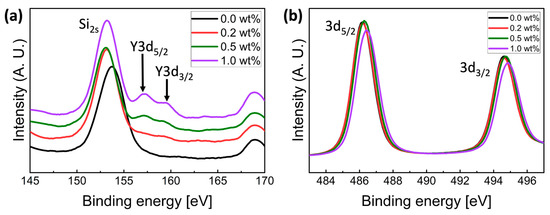
Figure 3.
XPS spectra for Y-doped SnO2 films, with different Ywt% in the (a) Y3d, and (b) Sn3d regions.
Figure 4 shows the O 1s XPS spectra of Y-doped SnO2 films as a function of Ywt%. The O 1s peak convoluted into two different Gaussian subpeaks, occurring at 529.9 and 531.8 eV. The dominant peak located at 529.9 eV was related to O2− ions binding with neighbor metal ions in the lattice (OL), and the peak located at 531.8 eV was related to O2− ions in oxygen vacancy regions (OV). The relative oxygen vacancy quantity was estimated with the area ratio of the convoluted subpeaks. With an increase in the wt% of Y, lower oxygen vacancy density was obtained. The OV/(OL+OV) ratios were 0.46 for pure SnO2, 0.45 for 0.2wt% Y-doped SnO2, 0.40 for 0.5wt% Y-doped SnO2, and 0.3 for 1.0wt% Y-doped SnO2, respectively. Obviously, the OV/(OL+OV) area ratio gradually decreased with the increase of Ywt%, indicating that the OV concentration was decreased by Y doping. Y3+ ions can act as carrier suppressors in SnO2 thin film systems, due to their lower electronegativity (1.22) and lower standard electrode potential (SEP) (−2.38 V). The increased bond strength of dopant-oxygen bond lead to decrease the oxygen vacancy, related to the carrier concentration in the metal oxide semiconductor system. For these reasons, Y is a stronger oxidizer than Sn. During the film formation step, fewer oxygen vacancies were formed in Y-doped SnO2 films compared to pure SnO2 films. Huh et al. found that Sn2+ binding in SnO2 leads to the formation of oxygen vacancy defects. Therefore, the reduction in the proportions of the SnO and OV peaks with Y content indicated a decrease in electron free carrier density and oxygen vacancy.
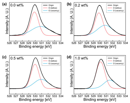
Figure 4.
Deconvoluted O1s XPS spectra for Y-doped SnO2 thin films with (a) 0.0, (b) 0.2, (c) 0.5, and (d) 1.0wt% Y annealed at 500 °C for 2 h.
Figure 5 shows the variation of the electrical properties of the fabricated Y-doped SnO2 thin film transistors using different Ywt% at gate voltages of −30 V to 30 V. Figure 5e shows the representative transfer curves (ID-VG) of SnO2 thin film transistors with different Ywt%. All the fabricated Y-doped SnO2 thin film transistors showed conventional n-type semiconductor characteristics. The field effect mobility in the saturation regime was calculated from the drain current equation, which is given as follows:
where Ci is the capacitance of gate insulator, W is the channel width, L is the channel length, and Vth is the threshold voltage. The extracted field effect mobilities in the saturation regime of the pristine, 0.2, 0.5, and 1.0 wt% Y-doped SnO2 thin film transistors were 12, 7.4, 1, and 0.7 cm2/Vs, respectively. When Ywt% increased, the on current and field effect mobility in the saturation regimes were decreased. The crystalline size of the semiconductor active channel layer strongly affects the on-current and field-effect mobility of thin film transistors. Larger crystalline size is helpful to improve device performance via the suppression of boundary scattering. However, based on GIXRD data, with increased Ywt%, the crystalline size of SnO2 semiconductor films was deceased. Decreased crystalline and strong grain boundary scattering also leads to degraded device performances [24]. It is well known that the main transport mechanism of metal oxide semiconductor systems is percolation conduction mechanism, which is improved by filling the trap state at high carrier concentrations [25]. The degraded field-effect mobility and on-current originated from a significant decrease in the free carrier concentration, originating from the oxygen vacancy in metal oxide semiconductors. In addition, the Y3+-Sn4+ substitution reaction might generate an extra hole carrier, leading to a decrease in free carrier concentration by compensating for electron carrier concentration [26]. In addition, the threshold voltage exhibited a positive shift, in particular, from 0.5 wt% Y. The fabricated devices showed enhancement mode operation. The reduced carrier concentration in the n-type semiconductor based thin film transistors induced higher Vth. The channel with a lower carrier concentration could be depleted easily and required more gate bias to turn on devices. In this study, these positive shifts in Vth originated from the reduced electron density in the SnO2 semiconductor active layer with an Ywt% increase.
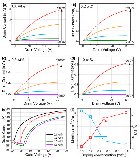
Figure 5.
Representative electrical characteristics of the fabricated Y-doped SnO2 thin film transistors: (a–d) ID-VD curves with 0.0, 0.2, 0.5, 1.0 wt% Y, respectively. (e) ID-VG curves at high VD (+30.0 V). (f) Y concentration dependence on the field effect mobility in saturation regime and Vth.
4. Conclusions
In this study, Y-doped SnO2 thin film transistors were successfully fabricated by means of sol-gel process. The effect of Y concentration on the structural, chemical, and electrical properties of sol-gel processed SnO2 films was investigated using GIXRD, SPM, and XPS. The corresponding electrical transport properties of the film were also evaluated. The dopant, Y, can successfully control the free carrier concentration by suppressing the formation of oxygen vacancy inside SnO2 semiconductors due to its lower electronegativity and SEP. With an increase of Ywt%, it was observed that the crystallinity and oxygen vacancy concentration decreased, and the operation mode of the SnO2 thin film transistor occurred from accumulation (normally on) to enhancement mode (normally off) with a positive Vth shift.
Author Contributions
Conceptualization, C.L. and J.J.; Experiments and data analysis, C.L., W.-Y.L., H.L. S.H.; Investigation, J.-H.B., I.-M.K., H.K., and K.K.; Writing—original draft preparation, C.L. and J.J.; Writing—Review & Editing, J.-H.B., I.-M.K., H.K., K.K. and J.J. All authors have read and agreed to the published version of the manuscript.
Funding
This research was supported by the Basic Science Research Program through the National Research Foundation of Korea (NRF) funded by the Ministry of Education (NRF-2016R1D1A3B03930896) and by the National Research Foundation of Korea (NRF) grant funded by the Korea government (MSIT) (2019R1F1A1059788).
Conflicts of Interest
The authors declare no conflict of interest.
References
- Nomura, K.; Ohta, H.; Takagi, A.; Kamiya, T.; Hirano, M.; Hosono, H. Room-temperature fabrication of transparent flexible thin-film transistors using amorphous oxide semiconductors. Nature 2004, 432, 488–492. [Google Scholar] [CrossRef] [PubMed]
- Yabuta, H.; Sano, M.; Abe, K.; Aiba, T.; Den, T.; Kumomi, H.; Nomura, K.; Kamiya, T.; Hosono, H. High-mobility thin-film transistor with amorphous InGaZnO4 channel fabricated by room temperature rf-magnetron sputtering. Appl. Phys. Lett. 2006, 89, 112123. [Google Scholar] [CrossRef]
- Tomai, S.; Nishimura, M.; Itose, M.; Matuura, M.; Kasami, M.; Matsuzaki, S.; Kawashima, H.; Utsuno, F.; Yano, K. High performance thin film transistor with amorphous In2O3–SnO2–ZnO channel layer. Jpn. J. Appl. Phys. 2012, 51, 03CB01. [Google Scholar] [CrossRef]
- Ebata, K.; Tomai, S.; Tsuruma, Y.; Iitsuka, T.; Matsuzaki, S.; Yano, K. High-mobility thin-film transistors with polycrystalline In–Ga–O channel fabricated by DC magnetron sputtering. Appl. Phys. Express 2012, 5, 011102. [Google Scholar] [CrossRef]
- Ellmer, K. Resistivity of polycrystalline zinc oxide films: Current status and physical limit. J. Phys. D Appl. Phys. 2001, 34, 3097–3108. [Google Scholar] [CrossRef]
- Wang, C.M.; Huang, C.C.; Kuo, J.C.; Sahu, D.R.; Huang, J.L. Effect of annealing temperature and oxygen flow in the properties of ion beam sputtered SnO2−x thin films. Materials 2015, 8, 5289–5297. [Google Scholar] [CrossRef]
- Das, S.; Jararaman, V. SnO2: A comprehensive review on structures and gas sensors. Prog. Mater. Sci. 2014, 66, 112–255. [Google Scholar] [CrossRef]
- Yang, D.; Yang, R.; Wang, K.; Wu, C.; Zhu, X.; Feng, J.; Ren, X.; Fang, G.; Priya, S.; Liu, S. High efficiency planar-type perovskite solar cells with negligible hysteresis using EDTA-complexed SnO2. Nat. Commun. 2018, 9, 3239. [Google Scholar] [CrossRef]
- Haxel, G.B.; Hedrick, J.B.; Orris, G.J. Rare Earth Elements—Critical Resources for High Technology; Fact Sheet 087-02; U.S. Geological Survey: Reston, VA, USA, 2002.
- Sun, J.J.; Lu, A.; Wang, L.; Hu, Y.; Wan, Q. High-mobility transparent thin-film transistors with an Sb-doped SnO2 nanocrystal channel fabricated at room temperature. Nanotechnology 2009, 20, 335204. [Google Scholar] [CrossRef]
- Ju, S.; Chen, P.; Zhou, C.; Ha, Y.-G.; Facchetti, A.; Marks, T.J.; Kim, S.K.; Mohammadi, S.; Janes, D.B. 1/f noise of SnO2 nanowire transistors. Appl. Phys. Lett. 2008, 92, 243120. [Google Scholar] [CrossRef]
- Fortunato, E.; Barquinha, P.; Pimentel, A.; Pereira, L.; Gonçalves, G.; Martins, R. Amorphous IZO TTFTs with saturation mobilities exceeding 100 cm2/Vs. Phys. Status Solidi 2007, 1, R34–R36. [Google Scholar] [CrossRef]
- Dehuff, N.L.; Kettenring, E.S.; Hong, D.; Chiang, H.Q.; Wager, J.F.; Hoffman, R.L.; Park, C.-H.; Keszler, D.A. Transparent thin-film transistors with zinc indium oxide channel layer. J. Appl. Phys. 2005, 97, 064505. [Google Scholar] [CrossRef]
- Wang, L.; Yoon, M.H.; Lu, G.; Yang, Y.; Facchetti, A.; Marks, T.J. High-performance transparent inorganic-organic hybrid thin-film n-type transistors. Nat. Mater. 2006, 5, 893–900. [Google Scholar] [CrossRef] [PubMed]
- Jang, J.; Kitsomboonloha, R.; Swisher, S.L.; Park, E.S.; Kang, H.; Subramanian, V. Transparent high-performance thin film transistors from solution-processed SnO2/ZrO2 gel-like precursors. Adv. Mater. 2013, 25, 1042–1047. [Google Scholar] [CrossRef] [PubMed]
- Jang, J.; Kang, H.; Chakravarthula, H.C.N.; Subramanian, V. Fully inkjet-printed transparent oxide thin film transistors using a fugitive wettability switch. Adv. Electron. Mater. 2015, 1, 1500086. [Google Scholar] [CrossRef]
- Jang, B.; Kim, T.; Lee, S.; Lee, W.Y.; Kang, H.; Cho, C.S.; Jang, J. High performance ultrathin SnO2 thin film transistors by sol-gel method. IEEE Electron Device Lett. 2018, 39, 1179–1182. [Google Scholar] [CrossRef]
- Jang, B.; Kim, T.; Lee, S.; Lee, W.Y.; Jang, J. Schottky nature of Au/SnO2 ultrathin film diode prepared by sol-gel method. IEEE Electron Device Lett. 2018, 39, 1732–1735. [Google Scholar] [CrossRef]
- Lee, W.Y.; Ha, S.H.; Lee, H.; Bae, J.H.; Jang, B.; Kwon, H.J.; Jang, J. Densification control as a method of improving air stability of thin film transistors based on sol-gel processed SnO2. IEEE Electron Device Lett. 2019, 40, 905–908. [Google Scholar] [CrossRef]
- Lee, H.; Ha, S.H.; Bae, J.H.; Kang, I.M.; Kim, K.; Lee, W.Y.; Jang, J. Effect of annealing ambient on SnO2 thin film transistors via an ethanol-based sol-gel route. Electronics 2019, 8, 995. [Google Scholar] [CrossRef]
- Kim, T.; Jang, B.; Lee, S.; Lee, W.Y.; Jang, J. Improved negative bias stress stability of sol-gel-processed Mg-doped In2O3 thin film transistors. IEEE Electron Device Lett. 2018, 39, 1872–1875. [Google Scholar] [CrossRef]
- Kim, T.; Jang, B.; Bae, J.H.; Park, H.; Cho, C.S.; Kwon, H.J.; Jang, J. Improvement in the performance of sol–gel processed In2O3 thin-film transistor depending on Sb dopant concentration. IEEE Electron Device Lett. 2017, 38, 1027–1030. [Google Scholar] [CrossRef]
- Lee, S.H.; Kwon, K.; Kim, K.; Yoon, J.S.; Choi, D.S.; Yoo, Y.; Kim, C.; Kang, S.; Kim, J.H. Electrical, structural, optical, and adhesive characteristics of aluminum-doped tin oxide thin films for transparent flexible thin-film transistor applications. Materials 2019, 12, 137. [Google Scholar] [CrossRef] [PubMed]
- Gupta, N.; Tyagi, B.P. On-current modeling of polycrystalline silicon thin-film transistors. Phys. Scr. 2005, 72, 339. [Google Scholar] [CrossRef]
- Kim, Y.S.; Park, C.H. Rich variety of defects in ZnO via an attractive interaction between o vacancies and zn interstitials: Origin of n-type doping. Phys. Rev. Lett. 2009, 102, 806403. [Google Scholar] [CrossRef]
- Joseph, J.; Mathew, V.; Abraham, K.E. Physical properties of Dy and La doped SnO2 thin films prepared by a cost effective vapour deposition technique. Cryst. Res. Technol. 2006, 41, 1020–1026. [Google Scholar] [CrossRef]


© 2020 by the authors. Licensee MDPI, Basel, Switzerland. This article is an open access article distributed under the terms and conditions of the Creative Commons Attribution (CC BY) license (http://creativecommons.org/licenses/by/4.0/).