HoneyComb ROS: A 6 × 6 Non-Blocking Optical Switch with Optimized Reconfiguration for ONoCs

 ,
,
Abstract
1. Introduction
- We propose a 6 × 6 reconfigurable non-blocking optical switch with a reduced number of OSE where routing combinations can be reconfigured using optimized reconfiguration to route any desired I/O link.
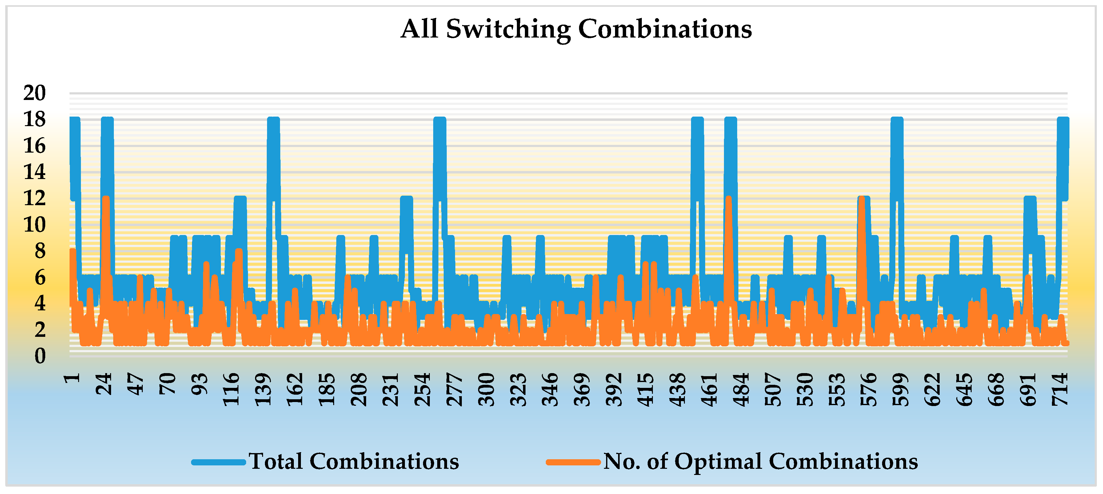
- We present a generic algorithm to find the optimal switching combination with the minimal number of OSE in an active, i.e., drop/bar state, which is used to complete the process of optimized reconfiguration to minimize the IL and power consumption. We identify a particular switching combination, where all OSEs are found in an inactive state that leads to minimum power consumption through optimized reconfiguration of the proposed HCROS.
- Further optimization significantly reduces the number of OSEs in comparison to other non-blocking switch architectures, which leads to minimized hardware cost and compact foot print of the HCROS topology while keeping the non-blocking feature intact.
- A comprehensive analysis for power consumption and insertion loss for all N! possible I/O links is also discussed in this article.
- Optimized: We use the term “optimized” for the 6-port HCROS optical switch with reduced OSEs as a result of optimization where some OSEs are replaced with waveguide crossings.
- Optimal: We defined the term “optimal” as the configuration for the minimum number of OSEs in a bar/drop state or more specifically, “optimal switching combination”. Since basic 2 × 2 micro-ring (MR)-based OSE consumes more power in a bar/drop state than in a cross/through state, also the insertion loss of 2 × 2 MR-based OSE is higher in a bar/drop state.
- “Optimized reconfiguration” is defined as a process of utilizing optimal switching combination (optimal state) to reconfigure OSEs in HCROS to reduce power consumption and minimize insertion loss while ensuring the input to output interconnections are unaffected.
- I/O link: An I/O links is defined as a set of particular “routing combinations” to connect the desired input to output.
- Routing combination: A routing combination consists of six optical paths to connect each input port to every output port for mapping a particular I/O link, hence it is responsible for transmission of data in parallel.
- The switching combination is the state of OSEs for a particular routing combination to map a particular I/O link.
2. Background
- Input signal from any input In should be routed to any output port On of the radix N optical switch.
- The link between any input In and output On pair should not block other input-output optical links in particular routing combinations of the radix N optical switch.
- For an N port non-blocking optical switch there exists N! switching states. For example, N = 6, it contains 6! = 720 possible switching states. For any switch to be non-blocking it should have N! routing states that remain intact, otherwise it would become blocking.
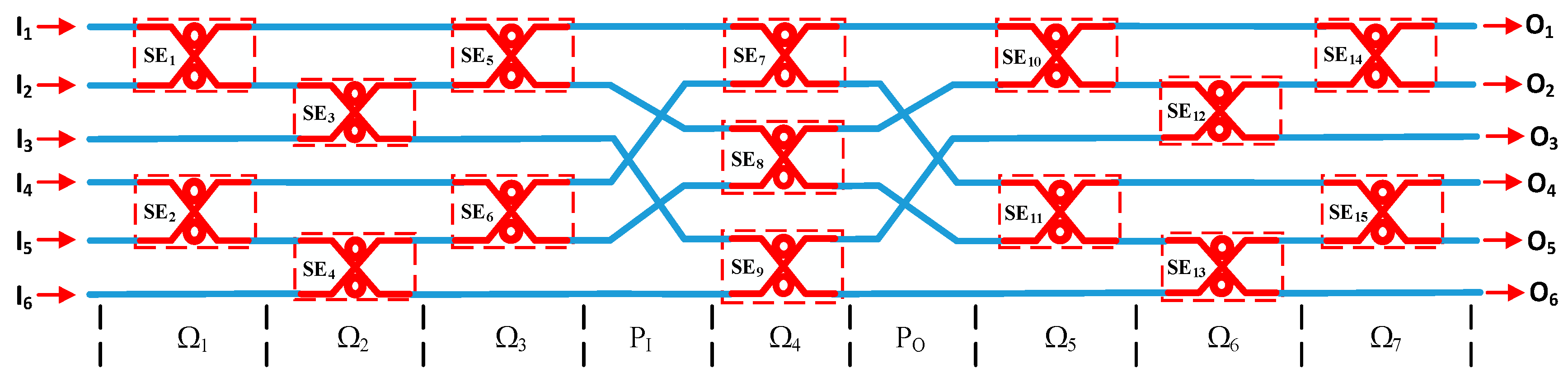
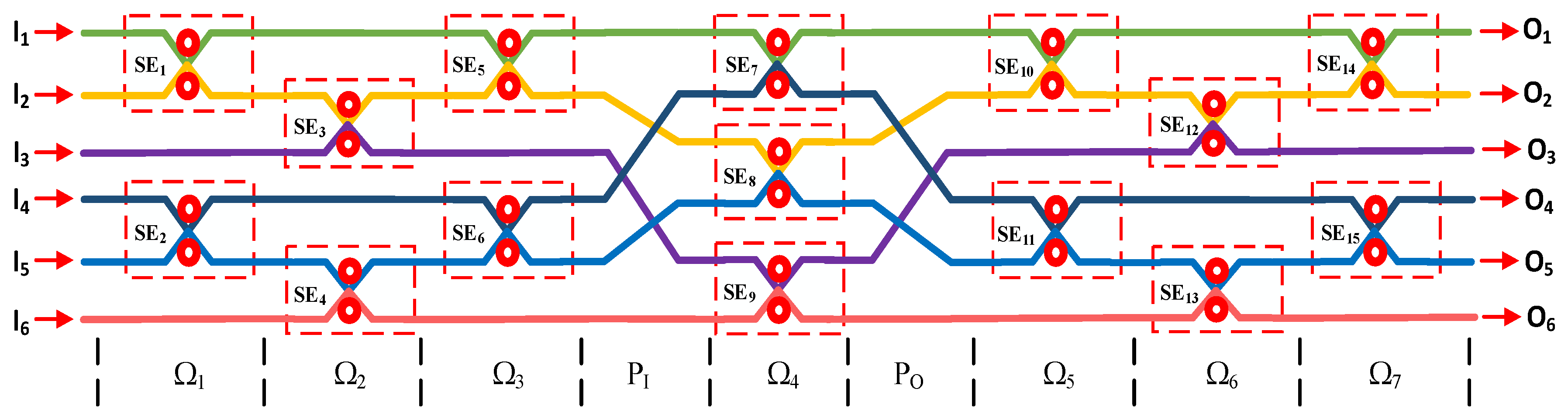
3. Switch Architecture
3.1. Six-Port Non-Blocking Reconfigurable Optical Switch Architecture
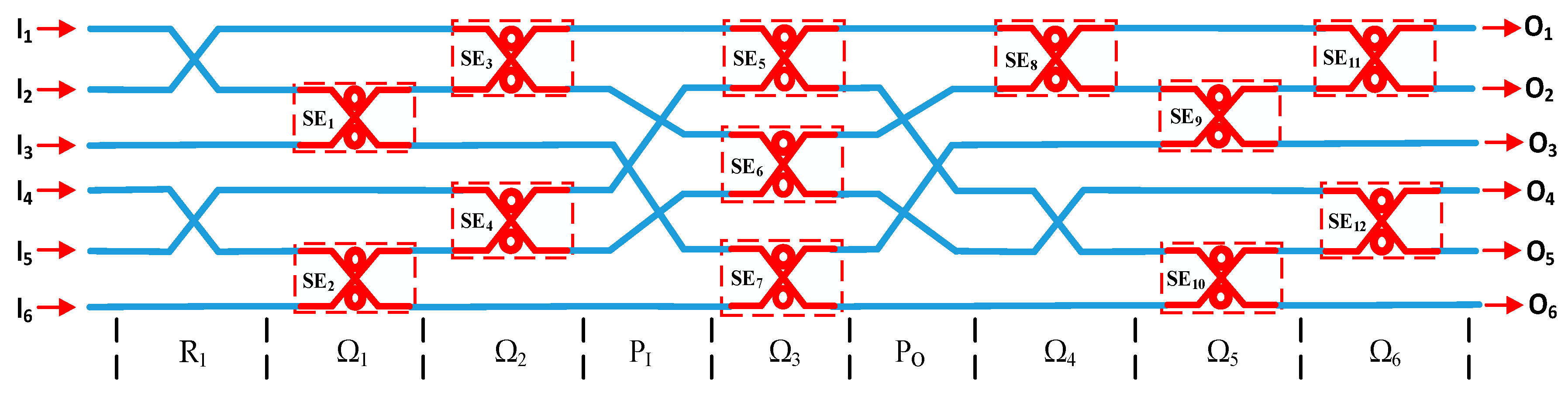
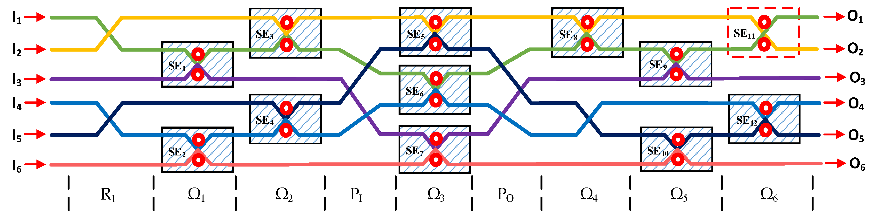
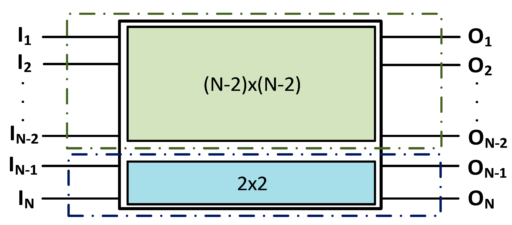
3.2. Optimized 6-Port Non-Blocking Reconfigurable Optical Switch Architecture
4. Mathematical Proof for the Non-Blocking Property of HCROS
- When I1 → O1 and I2 → O2;
- When I1 → O2 and I2 → O1;
5. Proposed Algorithm
5.1. Notations and Proposed Algorithm
- N: number of input-output ports
- s: number of stages
- ek: number of OSEs in each stage
- Ns: total number of OSEs
- St: possible switching states
- Md: Desired transfer matrix
- Ci: desired I/O link for particular routing combination
- Nc: total number of switching combinations for respective I/O link
- Nd: total number of combinations with least number of OSEs in drop/bar state
- Dc: optimal number of OSEs in drop/bar state
5.2. Analysis Using Proposed Algorithm-1 for HCROS
6. Comparisons, Analysis and Simulation Results
6.1. Calculation of Insertion Loss and Power Consumption for HCROS
6.2. Comparisons, Results and Analysis
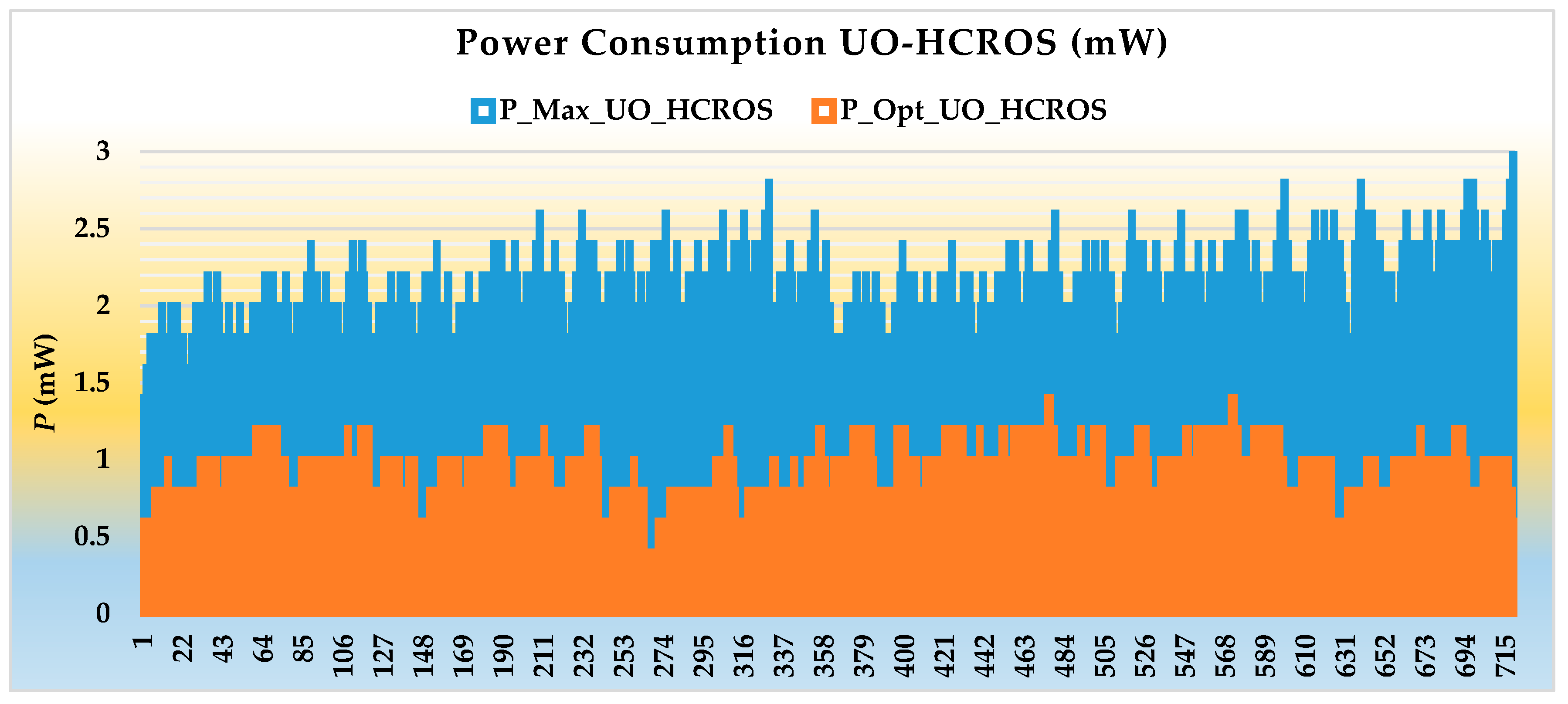
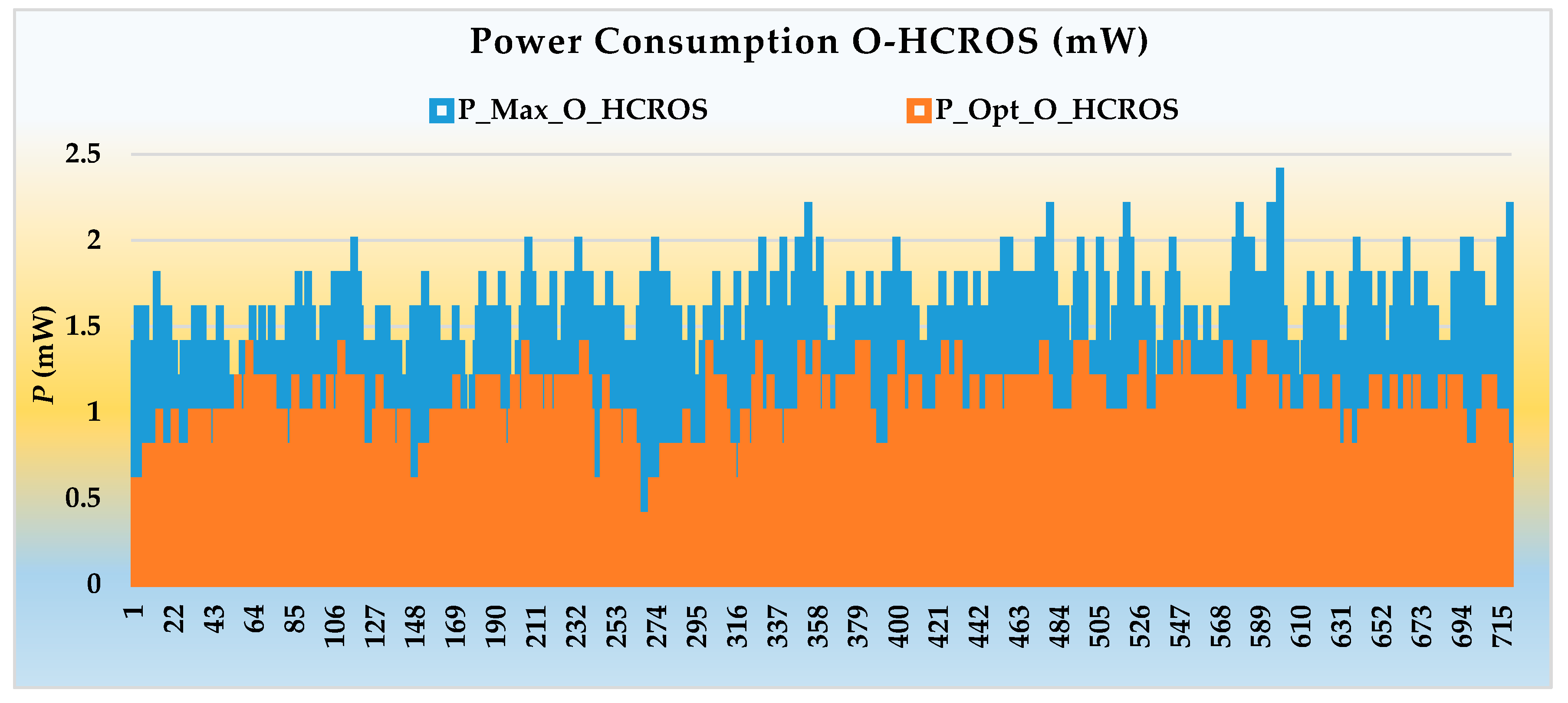
6.3. Power Consumption of HCROS
- PMax_UO_HCROS is the maximum power consumption in un-optimized HCROS
- PMax_O_HCROS is the maximum power consumption in optimized HCROS
- POpt_UO_HCROS is the optimal power consumption in un-optimized HCROS
- POpt_O_HCROS is the optimal power consumption in optimized HCROS
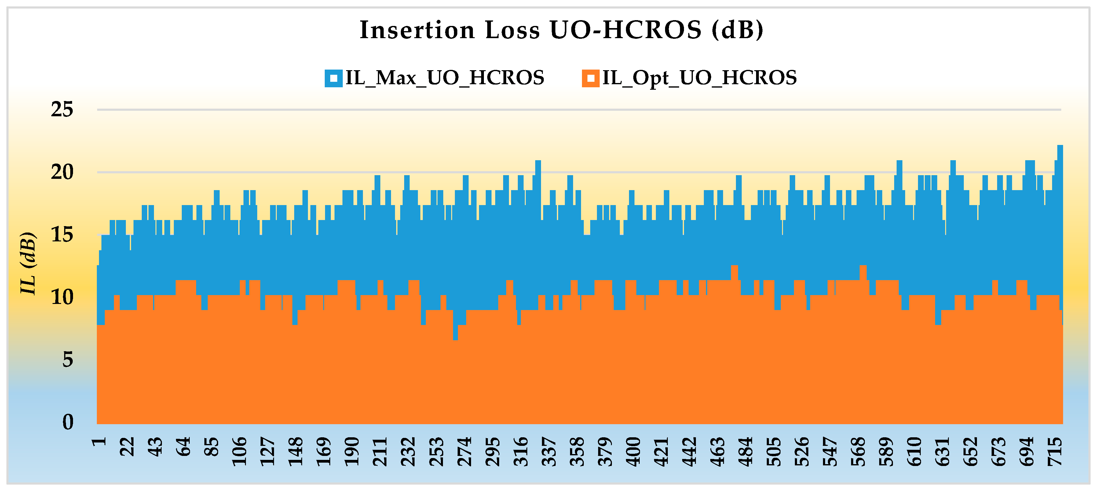
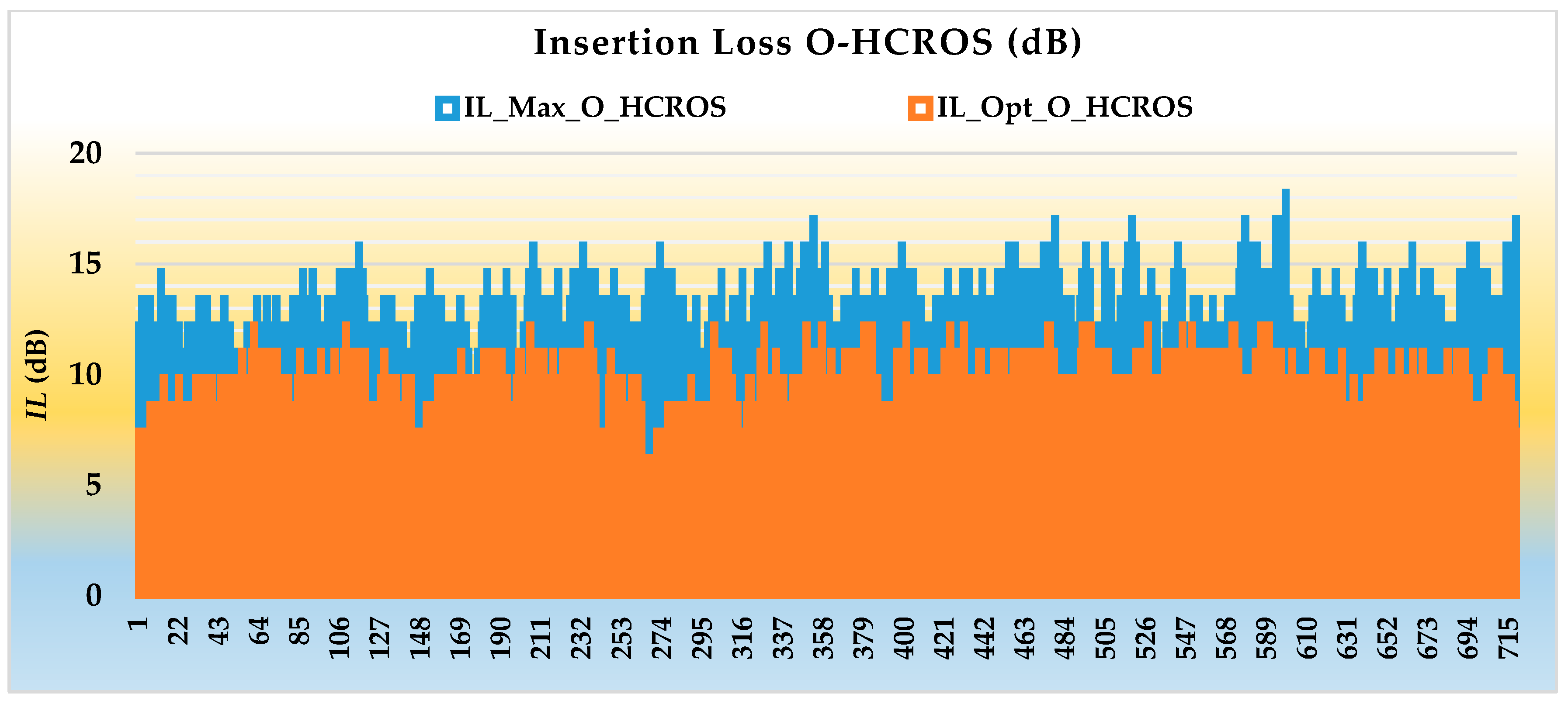
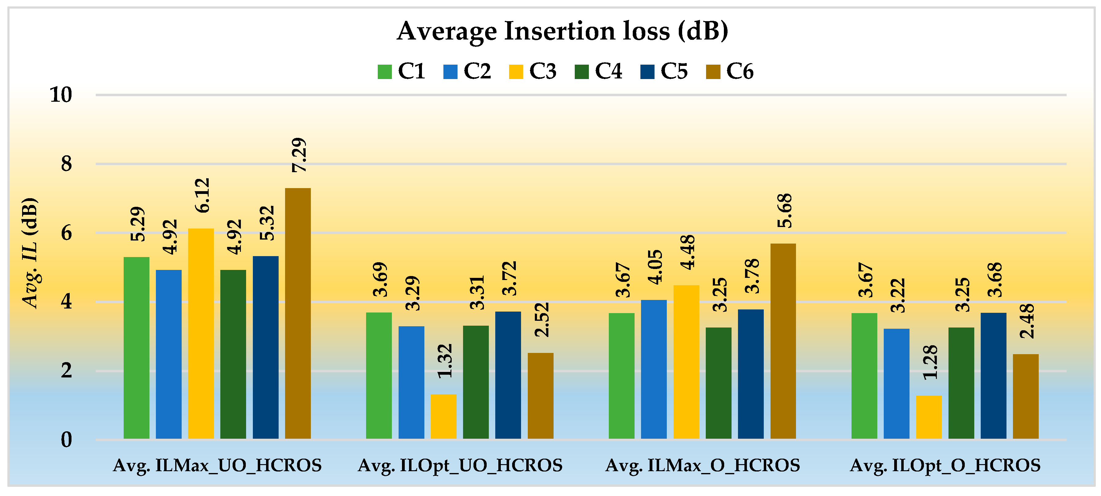
6.4. Insertion Loss in HCROS
- ILMax_UO_HCROS is the maximum insertion loss in un-optimized HCROS
- ILMax_O_HCROS is the maximum insertion loss in optimized HCROS
- ILOpt_UO_HCROS is the optimal insertion loss in un-optimized HCROS
- ILOpt_O_HCROS is the optimal insertion loss in optimized HCROS
7. Conclusions
Author Contributions
Funding
Acknowledgments
Conflicts of Interest
References
- Arakawa, Y.; Nakamura, T.; Urino, Y.; Fujita, T. Silicon photonics for next generation system integration platform. IEEE Commun. Mag. 2013, 51, 72–77. [Google Scholar] [CrossRef]
- Nikolova, D.; Rumley, S.; Calhoun, D.; Li, Q.; Hendry, R.; Samadi, P.; Bergman, K. Scaling silicon photonic switch fabrics for data center interconnection networks. Opt. Express 2015, 23, 1159–1175. [Google Scholar] [CrossRef] [PubMed]
- Ro, Y.; Lee, E.; Ahn, J.H. Evaluating the Impact of Optical Interconnects on a Multi-Chip Machine-Learning Architecture. Electronics 2018, 7, 130. [Google Scholar] [CrossRef]
- Kayarkar, A.V.; Khurge, D.S. Router Architecture for the Interconnection Network: A Review. In Proceedings of the 2016 2nd International Conference on Computing, Communication, Control and Automation (ICCUBEA), Pune, India, 12–13 August 2016. [Google Scholar]
- Shacham, A.; Bergman, K.; Carloni, L.P. Photonic Networks-on-Chip for Future Generations of Chip Multiprocessors. IEEE Trans. Comput. 2008, 57, 1246–1260. [Google Scholar] [CrossRef]
- Fusella, E.; Cilardo, A. Lighting up On-Chip Communications with Photonics: Design Tradeoffs for Optical NoC Architectures. IEEE Circuits Syst. Mag. 2016, 16, 4–14. [Google Scholar] [CrossRef]
- Thraskias, C.A.; Lallas, E.N.; Neumann, N.; Schares, L.; Offrein, B.J.; Henker, R.; Plettemeier, D.; Ellinger, F.; Leuthold, J.; Tomkos, I. Survey of Photonic and Plasmonic Interconnect Technologies for Intra-Datacenter and High-Performance Computing Communications. IEEE Commun. Surv. Tutor. 2018, 20, 2758–2783. [Google Scholar] [CrossRef]
- Rumley, S.; Bahadori, M.; Polster, R.; Hammond, S.D.; Calhoun, D.M.; Wen, K.; Rodrigues, A.; Bergman, K. Optical interconnects for extreme scale computing systems. Parallel Comput. 2017, 64, 65–80. [Google Scholar] [CrossRef]
- Werner, S.; Navaridas, J.; Luján, M. A Survey on Optical Network-on-Chip Architectures. ACM Comput. Surv. 2017, 50, 1–37. [Google Scholar] [CrossRef]
- Yahya, M.R.; Wu, N.; Yan, G.; Yasir, Y. Review of Photonic and Hybrid on Chip Interconnects for MPSoCs in IoT Paradigm. In Proceedings of the 2018 21st Saudi Computer Society National Computer Conference (NCC), Riyadh, Saudi Arabiam, 25–26 April 2018; pp. 1–6. [Google Scholar]
- Zhou, T.; Jia, H.; Dai, J.; Yang, S.; Zhang, L.; Fu, X.; Yang, L. Rearrangeable-Nonblocking Five-Port Silicon Optical Switch for 2-D-Mesh Network on Chip. IEEE Photon. J. 2018, 10, 1–8. [Google Scholar] [CrossRef]
- Guo, P.; Hou, W.; Guo, L.; Yang, Q.; Ge, Y. Low Insertion Loss and Non-Blocking Microring-Based Optical Router for 3D Optical Network-on-Chip. IEEE Photon. J. 2018, 10, 1–10. [Google Scholar] [CrossRef]
- Jia, H.; Zhou, T.; Fu, X.; Ding, J.; Zhang, L.; Yang, L. Four-port mode-selective silicon optical router for on-chip optical interconnect. Opt. Express 2018, 26, 9740–9748. [Google Scholar] [CrossRef] [PubMed]
- Zhao, Y.; Jia, H.; Ding, J.; Zhang, L.; Fu, X.; Yang, L. Five-port silicon optical router based on Mach-Zehnder optical switches for photonic networks-on-chip. J. Semicond. 2016, 37, 114008. [Google Scholar] [CrossRef]
- Zhu, K.; Zhang, B.; Tan, W.; Gu, H. Votex: A non-blocking optical router design for 3D Optical Network on Chip. In Proceedings of the 2015 14th International Conference on Optical Communications and Networks (ICOCN), Nanjing, China, 3–5 July 2015; pp. 1–3. [Google Scholar]
- Jia, H.; Zhao, Y.; Zhang, L.; Chen, Q.; Ding, J.; Fu, X.; Yang, L. 5-port optical router based on Si microring optical switches for photonic networks-on-chip. IEEE Photon. Technol. Lett. 2016, 28, 947–950. [Google Scholar] [CrossRef]
- Dupuis, N.; Lee, B.G.; Rylyakov, A.V.; Kuchta, D.M.; Baks, C.W.; Orcutt, J.S.; Gill, D.M.; Green, W.M.J.; Schow, C.L. Modeling and Characterization of a Nonblocking 4×4 Mach–Zehnder Silicon Photonic Switch Fabric. J. Lightwave Technol. 2015, 33, 4329–4337. [Google Scholar] [CrossRef]
- Sathyadevaki, R.; Sundar, D.S.; Raja, A.S. Photonic crystal 4 × 4 dynamic hitless routers for integrated photonic NoCs. Photon. Netw. Commun. 2018, 36, 82–95. [Google Scholar] [CrossRef]
- Lipson, M.; Sherwood-Droz, N.; Poitras, C.B.; Biberman, A.; Lee, B.G.; Bergman, K. High-Speed 2 × 2 Switch for Multiwavelength Silicon-Photonic Networks-On-Chip. J. Lightwave Technol. 2009, 27, 2900–2907. [Google Scholar] [CrossRef]
- Jinguji, K.; Takato, N.; Sugita, A.; Kawachi, M. MachZehnder interferometer type opticalwaveguide coupler with wavelength-flattened coupling ratio. Electron. Lett. 1990, 26, 1326–1327. [Google Scholar] [CrossRef]
- Liang, L.; Zhang, K.; Zheng, C.T.; Zhang, X.; Qin, L.; Ning, Y.Q.; Zhang, D.M.; Wang, L.J. N × N Reconfigurable Nonblocking Polymer/Silica Hybrid Planar Optical Switch Matrix Based on Total-Internal-Reflection Effect. IEEE Photon. J. 2017, 9, 1–11. [Google Scholar] [CrossRef]
- Geng, M.; Tang, Z.; Chang, K.; Huang, X.; Zheng, J. N-port strictly non-blocking optical router based on Mach-Zehnder optical switch for photonic networks-on-chip. Opt. Commun. 2017, 383, 472–477. [Google Scholar] [CrossRef]
- Chen, Q.; Zhang, F.; Ji, R.; Zhang, L.; Yang, L. Universal method for constructing N-port non-blocking optical router based on 2 × 2 optical switch for photonic networks-on-chip. Opt. Express 2014, 22, 12614–12627. [Google Scholar] [CrossRef]
- Min, R.; Ji, R.; Yang, L.; Zhang, L.; Tian, Y.; Ding, J.; Chen, H.; Lu, Y.; Zhou, P.; Zhu, W. A universal method for constructing N-port non-blocking optical router based on microring resonators. J. Lightwave Technol. 2012, 30, 3736–3741. [Google Scholar] [CrossRef]
- Zhou, T.; Jia, H. Method to optimize optical switch topology for photonic network-on-chip. Opt. Commun. 2018, 413, 230–235. [Google Scholar] [CrossRef]
- Lin, B.C.; Chen, S.; Huang, Y.; Lea, C.T. Power Minimization in Microring-Based Benes Networks. IEEE Trans. Commun. 2018, 66, 3517–3525. [Google Scholar] [CrossRef]
- Lee, B.G.; Dupuis, N. Silicon Photonic Switch Fabrics: Technology and Architecture. J. Lightwave Technol. 2019, 37, 6–20. [Google Scholar] [CrossRef]
- Pattavina, A. Switching Theory—Architectures and Performance in Broadband ATM Networks; John Wiley & Sons Ltd.: Hoboken, NJ, USA, 1998; ISBN 0471963380. [Google Scholar]
- Benes, V. Algebraic and Topological Properties of Connecting Networks. Bell Syst. Tech. J. 1962, 41, 1249–1274. [Google Scholar] [CrossRef]
- Spanke, R.A.; Beneš, V.E. N-stage planar optical permutation network. Appl. Opt. 1987, 26, 1226–1229. [Google Scholar] [CrossRef]
- DasMahapatra, P.; Stabile, R.; Rohit, A.; Williams, K.A. Optical Crosspoint Matrix Using Broadband Resonant Switches. IEEE J. Sel. Top. Quantum Electron. 2014, 20, 1–10. [Google Scholar] [CrossRef]
- Shimoe, T. Path-independent insertion loss optical space switch. In Proceedings of the Optical Fiber Communication Conference, Reno, NV, USA, 19 January 1987. paper WB2. [Google Scholar]
- Ortín-Obón, M.; Suárez-Gracia, D.; Villarroya-Gaudó, M.; Izu, C.; Viñals-Yúfera, V. Analysis of network-on-chip topologies for cost-efficient chip multiprocessors. Microprocess. Microsyst. 2016, 42, 24–36. [Google Scholar] [CrossRef]
- Chittamuru, S.V.R.; Dang, D.; Pasricha, S.; Mahapatra, R.N. BiGNoC: Accelerating Big Data Computing with Application-Specific Photonic Network-on-Chip Architectures. IEEE Trans. Parallel Distrib. Syst. 2018, 29, 2402–2415. [Google Scholar] [CrossRef]
- Huang, L.; Wang, K.; Qi, S.; Gu, H.; Yang, Y. Panzer: A 6 × 6 photonic router for optical network on chip. IEICE Electron. Express 2016, 13, 20160719. [Google Scholar] [CrossRef]
- Yaghoubi, E.; Reshadi, M.; Hosseinzadeh, M. Mach–Zehnder-based optical router design for photonic networks on chip. Opt. Eng. 2015, 54, 035102. [Google Scholar] [CrossRef]
- Yahya, M.R.; Wu, N.; Yan, G.; Ge, F.; Ahmed, T. RoR: A low insertion loss design of rearrangeable hybrid photonic-plasmonic 6 × 6 non-blocking router for ONoCs. IEICE Electron. Express 2019, 16, 1–5. [Google Scholar] [CrossRef]
- Yuen, P.-H.; Chen, L.-K. Optimization of Microring-Based Interconnection by Leveraging the Asymmetric Behaviors of Switching Elements. J. Lightwave Technol. 2013, 31, 1585–1592. [Google Scholar] [CrossRef]
- Yang, Y.; Chen, K.; Gu, H.; Zhang, B.; Zhu, L. TAONoC: A Regular Passive Optical Network-on-Chip Architecture Based on Comb Switches. IEEE Trans. Very Large Scale Integr. Syst. 2018, 27, 954–963. [Google Scholar] [CrossRef]
- Zhang, L.; Tan, X.; Yang, M.; Qi, M.; Hu, T.; Yang, J. On-Chip Wavelength-Routed Photonic Networks with Comb Switches. In Proceedings of the 9th International Conference on Group IV Photonics (GFP), San Diego, CA, USA, 29–31 August 2012; Volume 14, pp. 279–281. [Google Scholar]
- Jia, H.; Zhou, T.; Zhao, Y.; Xia, Y.; Dai, J.; Zhang, L.; Ding, J.; Fu, X.; Yang, L. Six-port optical switch for cluster-mesh photonic network-on-chip. Nanophotonics 2018, 7, 827–835. [Google Scholar] [CrossRef]
- Jajszczyk, A. Rearrangeable Clos Networks: Fifty Years of the Theory Evolution. IEEE Commun. Mag. 2003, 41, 28–33. [Google Scholar] [CrossRef]
- Lin, B.C. Rearrangeable W-S-W Elastic Optical Networks Generated by Graph Approaches. J. Opt. Commun. Netw. 2018, 10, 675–685. [Google Scholar] [CrossRef]
- Bogaerts, W.; Van Thourhout, D.; Dumon, P.; Baets, R. Low-loss, low-cross-talk crossings for silicon-on-insulator nanophotonic waveguides. Opt. Lett. 2007, 32, 2801–2803. [Google Scholar] [CrossRef]


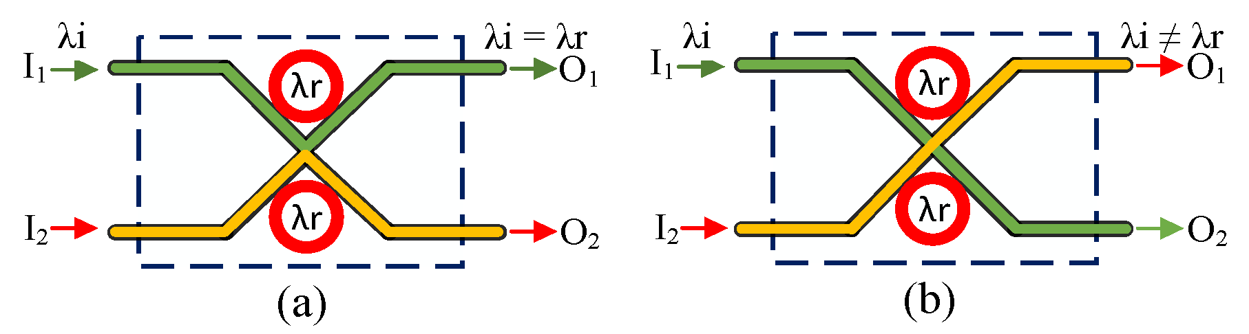
| Input | Output | MR State | Wavelength λi |
|---|---|---|---|
| I1 | O1 | DB * | λi = λr |
| I2 | O2 | DB * | λi = λr |
| I1 | O2 | TC * | λi ≠ λr |
| I2 | O1 | TC * | λi ≠ λr |
| I/O Links | Routing Combinations |
|---|---|
| SC1 | I1 → O2; I2 → O3; I3 → O4; I4 → O5; I5 → O6; I6 → O1; |
| SC2 | I1 → O3; I2 → O4; I3 → O5; I4 → O6; I5 → O1; I6 → O2; |
| SC3 | I1 → O4; I2 → O5; I3 → O6; I4 → O1; I5 → O2; I6 → O3; |
| SC4 | I1 → O5; I2 → O6; I3 → O1; I4 → O2; I5 → O3; I6 → O4; |
| SC5 | I1 → O6; I2 → O1; I3 → O2; I4 → O3; I5 → O4; I6 → O5; |
| SC6 | I1 → O1; I2 → O2; I3 → O3; I4 → O4; I5 → O5; I6 → O6; |
| I/O Links | SE1 | SE2 | SE3 | SE4 | SE5 | SE6 | SE7 | SE8 | SE9 | SE10 | SE11 | SE12 | SE13 | SE14 | SE15 |
|---|---|---|---|---|---|---|---|---|---|---|---|---|---|---|---|
| SC1 | DB | DB | DB | DB | DB | DB | DB | DB | TC | DB | DB | TC | TC | TC | TC |
| SC2 | DB | DB | DB | DB | DB | DB | DB | TC | TC | TC | TC | TC | TC | DB | DB |
| SC3 | DB | DB | DB | DB | DB | DB | TC | TC | TC | DB | DB | DB | DB | DB | DB |
| SC4 | DB | DB | DB | DB | DB | DB | TC | TC | DB | DB | DB | TC | TC | TC | TC |
| SC5 | DB | DB | DB | DB | DB | DB | TC | DB | DB | TC | TC | TC | TC | DB | DB |
| SC6 | DB | DB | DB | DB | DB | DB | DB | DB | DB | DB | DB | DB | DB | DB | DB |
| I/O Links | SE1 | SE2 | SE3 | SE4 | SE5 | SE6 | SE7 | SE8 | SE9 | SE10 | SE11 | SE12 |
|---|---|---|---|---|---|---|---|---|---|---|---|---|
| SC1 | DB | DB | DB | DB | DB | DB | TC | TC | TC | TC | TC | TC |
| SC2 | TC | TC | DB | DB | TC | TC | DB | DB | DB | DB | DB | TC |
| SC3 | DB | DB | DB | DB | TC | TC | TC | DB | DB | DB | TC | DB |
| SC4 | DB | DB | DB | DB | TC | TC | DB | TC | TC | TC | TC | TC |
| SC5 | TC | TC | DB | DB | DB | DB | TC | DB | DB | DB | DB | TC |
| SC6 | DB | DB | DB | DB | DB | DB | DB | DB | DB | DB | TC | DB |
| Inputs:N, s, ek, Ci |
| Outputs:Nc, Nd, Dc |
| Procedure: |
| 1. Determine Ns = |
| 2. Find St = 2Ns |
| 3. Define ETs and EDs using Equation (3) |
| 4. Compute Md for Ci using Equation (4) and Table 2 |
| 5. Set Nc = 0 to find total number of combinations |
| 6. Loop i = 1 to St |
| 7. Choose Ci. |
| 8. Loop j = 1 to Ns |
| 9. if (Ci(j) = 0) |
| 10. SE(j) = ETs using Equation (1) |
| 11. else |
| 12. SE(j) = EDs using Equation (2) |
| 13. end |
| 14. Get Ω1, Ω2, … ΩS using SE(j) for every switching stage using Equation (5). |
| 15. Calculate M = Ω1, Ω2, … ΩS using Equation (4) |
| 16. If (M = Md) |
| 17. Nc = Nc + 1 |
| 18. Store Ci |
| 19. else |
| 20. Ignore Ci. |
| 21. Determine Nd. |
| 22. Find Dc = Ci (min(ED)). |
| 23. end |
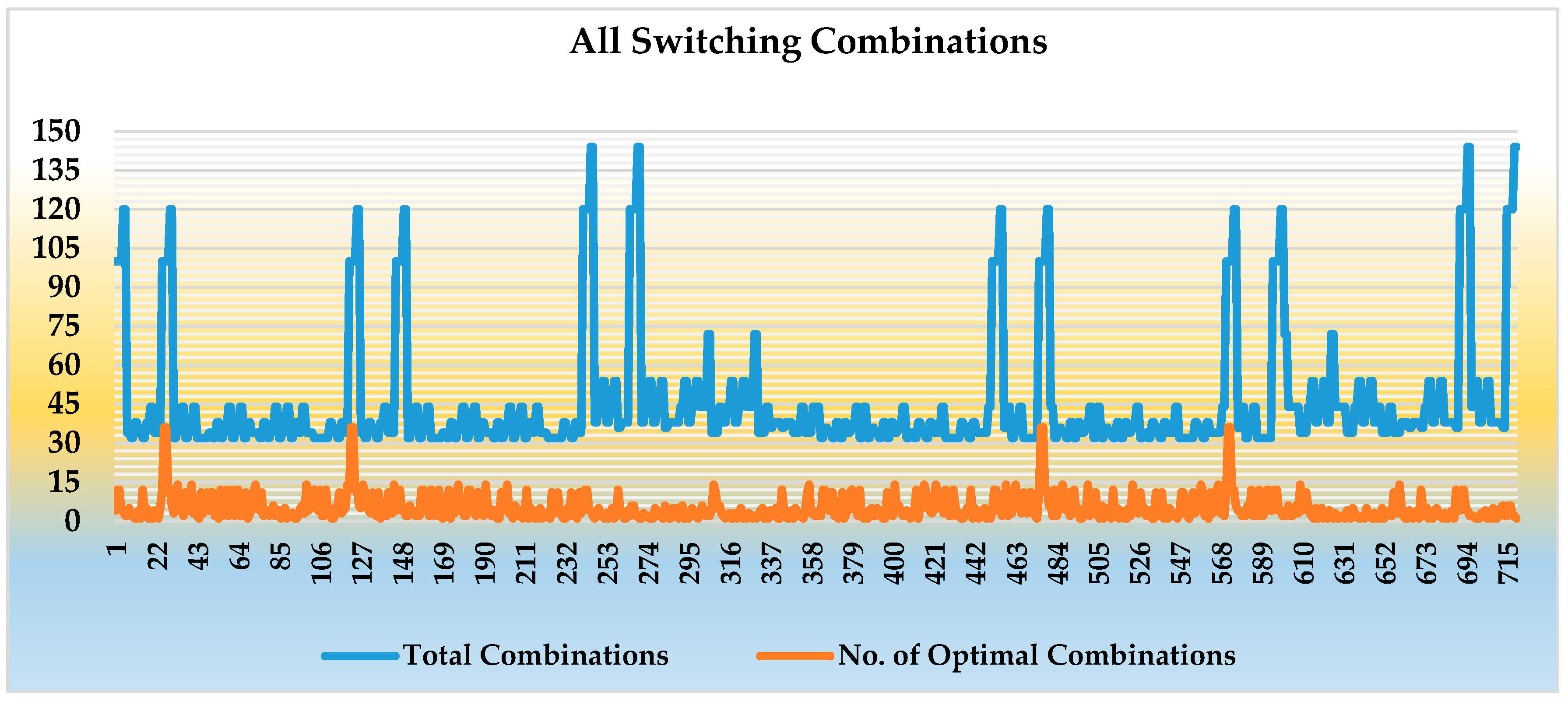
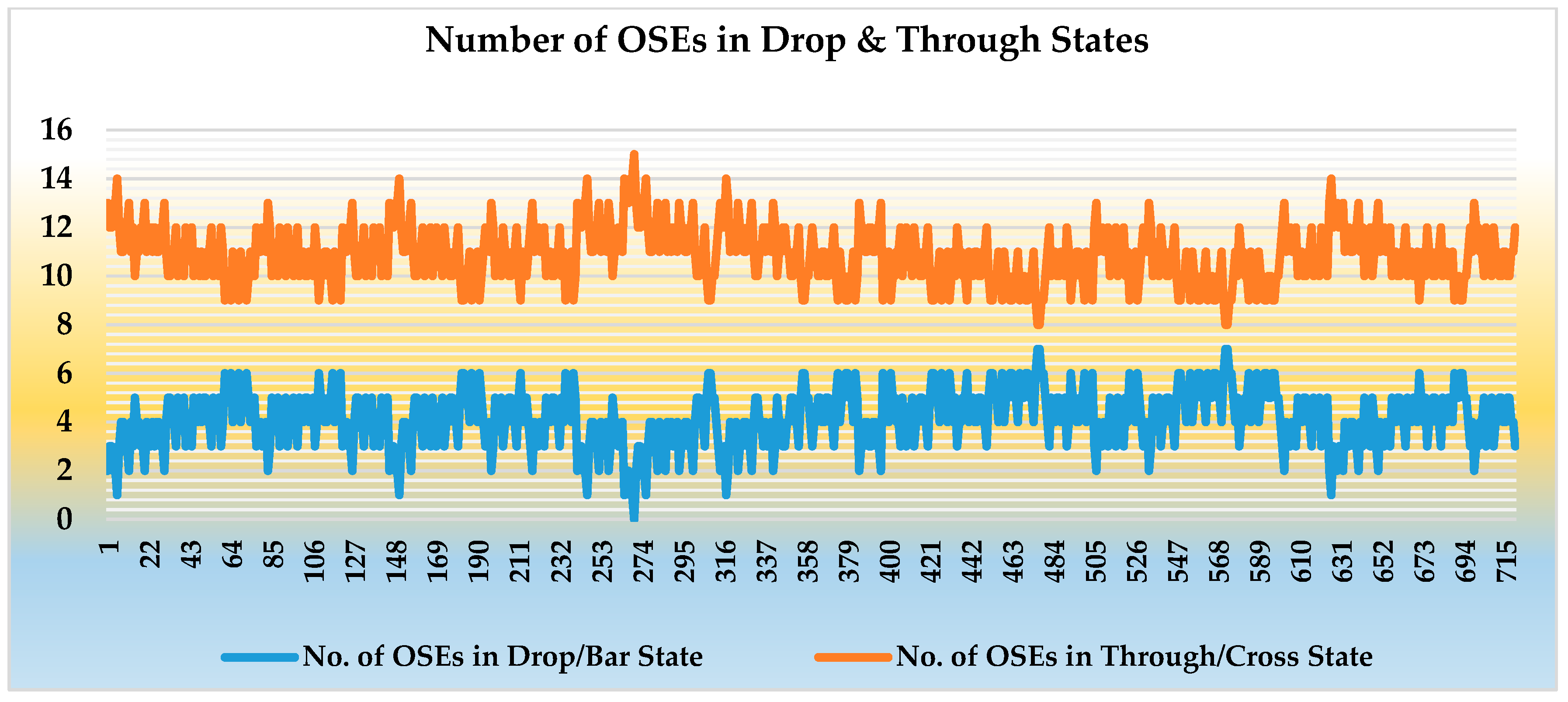
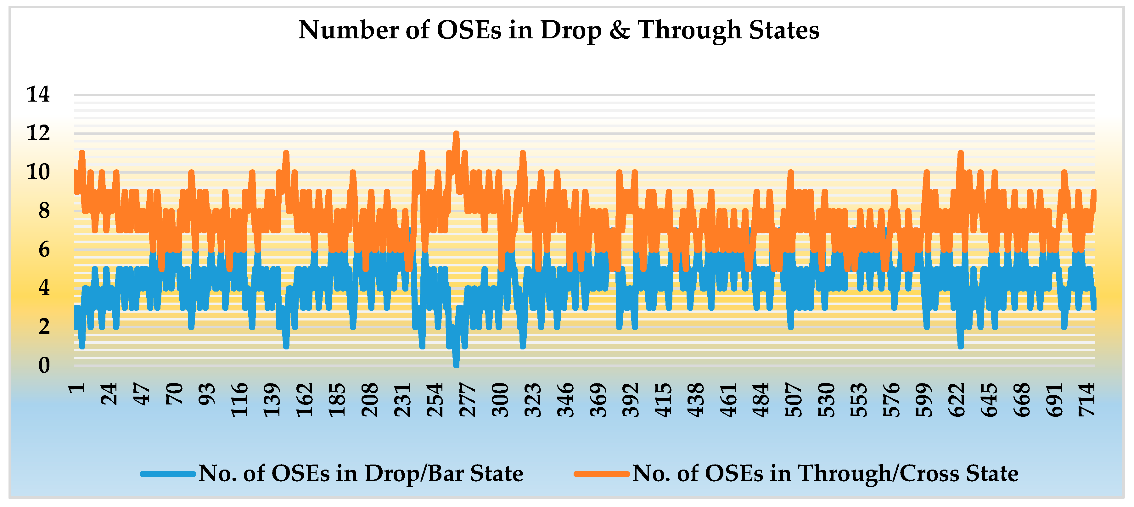
| I/O Links | Total Possible Combinations | No. of Optimal Combinations | No. of OSEs in Drop/Bar State | No. of OSEs in Through/Cross State |
|---|---|---|---|---|
| SC1 | 34 | 14 | 6 | 9 |
| SC2 | 34 | 14 | 5 | 10 |
| SC3 | 144 | 1 | 0 | 15 |
| SC4 | 34 | 14 | 5 | 10 |
| SC5 | 34 | 14 | 6 | 9 |
| SC6 | 144 | 1 | 3 | 12 |
| I/O Links | Total Combinations | No. of Optimal Combinations | No. of OSEs in Drop/Bar State | No. of OSEs in Through/Cross State |
|---|---|---|---|---|
| SC1 | 3 | 3 | 6 | 6 |
| SC2 | 9 | 7 | 5 | 7 |
| SC3 | 18 | 1 | 0 | 12 |
| SC4 | 3 | 3 | 5 | 7 |
| SC5 | 9 | 7 | 6 | 6 |
| SC6 | 18 | 1 | 3 | 9 |
| Parameters | Drop/Bar State | Through/Cross State |
|---|---|---|
| Power Consumption of OSE | PD | PT |
| 200 µW [38] | 0 W [38] | |
| Insertion Loss of OSE | ILD | ILT |
| 1.4 dB [38] | 0.2 dB [38] | |
| IL of Waveguide Crossing | ILC | |
| 0.16 dB [44] | ||
| Switch Topology | Total OSEs | Waveguide Crossings | Max. OSEs in one Path |
|---|---|---|---|
| PILOSS [32] | 36 | 30 | 6 |
| Cross Switch Matrix [31] | 36 | 0 | 11 |
| Reference [24] | 24 | 24 | 4 |
| Spanke-Benes [30] | 15 | 0 | 6 |
| Reference [36] | 12 | 11 | 4 |
| RoR [37] | 15 | 8 | 7 |
| HCROS Un-Optimized | 15 | 6 | 7 |
| HCROS Optimized | 12 | 9 | 5 |
| Switch Topology | Maximum Power (mW) | Maximum Insertion Loss (dB) | Minimum Insertion Loss (dB) |
|---|---|---|---|
| PILOSS [32] | 7.2 | 55.2 | 12 |
| Cross Switch Matrix [31] | 7.2 | 50.4 | 7.2 |
| Spanke-Benes [30] | 3.0 | 21 | 3.0 |
| RoR [37] | 3.0 | 22.28 | 4.28 |
| HCROS Un-Optimized | 3.0 | 21.96 | 3.96 |
| HCROS Optimized | 2.4 | 18.24 | 3.84 |
| I/O Links | HCROS Un-Optimized | HCROS Optimized | ||
|---|---|---|---|---|
| Maximum (PMax_UO_HCROS) | Optimal (POpt_UO_HCROS) | Maximum (PMax_O_HCROS) | Optimal (POpt_O_HCROS) | |
| SC1 | 10*PD + 5*PT | 6*PD + 9*PT | 6*PD + 6*PT | 6*PD + 6*PT |
| SC2 | 9*PD + 6*PT | 5*PD + 10*PT | 7*PD + 5*PT | 5*PD + 7*PT |
| SC3 | 12*PD + 3*PT | 15*PT | 8*PD + 4*PT | 12*PT |
| SC4 | 9*PD + 6*PT | 5*PD + 10*PT | 5*PD + 7*PT | 5*PD + 7*PT |
| SC5 | 10*PD + 5*PT | 6*PD + 9*PT | 8*PD + 4*PT | 6*PD + 6*PT |
| SC6 | 15*PD | 3*PD + 12*PT | 11*PD + 1*PT | 3*PD + 9*PT |
| I/O Links | HCROS Un-Optimized | HCROS Optimized | ||
|---|---|---|---|---|
| Maximum (ILMax_UO_HCROS) | Optimal (ILOpt_UO_HCROS) | Maximum (ILMax_O_HCROS) | Optimal (ILOpt_O_HCROS) | |
| SC1 | 6*ILC + 10*ILD + 5*ILT | 6*ILC + 6*ILD + 9*ILT | 9*ILC + 6*ILD + 6*ILT | 9*ILC + 6*ILD + 6*ILT |
| SC2 | 6*ILC + 9*ILD + 6*ILT | 6*ILC + 5*ILD + 10*ILT | 9*ILC + 7*ILD + 5*ILT | 9*ILC + 5*ILD + 7*ILT |
| SC3 | 6*ILC + 12*ILD + 3*ILT | 6*ILC + 15*ILT | 9*ILC + 8*ILD + 4*ILT | 9*ILC + 12*ILT |
| SC4 | 6*ILC + 9*ILD + 6*ILT | 6*ILC + 5*ILD + 10*ILT | 9*ILC + 5*ILD + 7*ILT | 9*ILC + 5*ILD + 7*ILT |
| SC5 | 6*ILC + 10*ILD + 5*ILT | 6*ILC + 6*ILD + 9*ILT | 9*ILC + 8*ILD + 4*ILT | 9*ILC + 6*ILD + 6*ILT |
| SC6 | 6*ILC + 15*ILD | 6*ILC + 3*ILD + 12*ILT | 9*ILC + 11*ILD + 1*ILT | 9*ILC + 3*ILD + 9*ILT |
| Parameter | HCROS Un-Optimized | HCROS Optimized | |||
|---|---|---|---|---|---|
| Power (mW) | Maximum/Minimum | Maximum (PMax_UO_HCROS) | Optimal (POpt_UO_HCROS) | Maximum (PMax_O_HCROS) | Optimal (POpt_O_HCROS) |
| Max. Power | 3.0 | 1.4 | 2.4 | 1.4 | |
| Min. Power | 1.2 | 0 | 0.6 | 0 | |
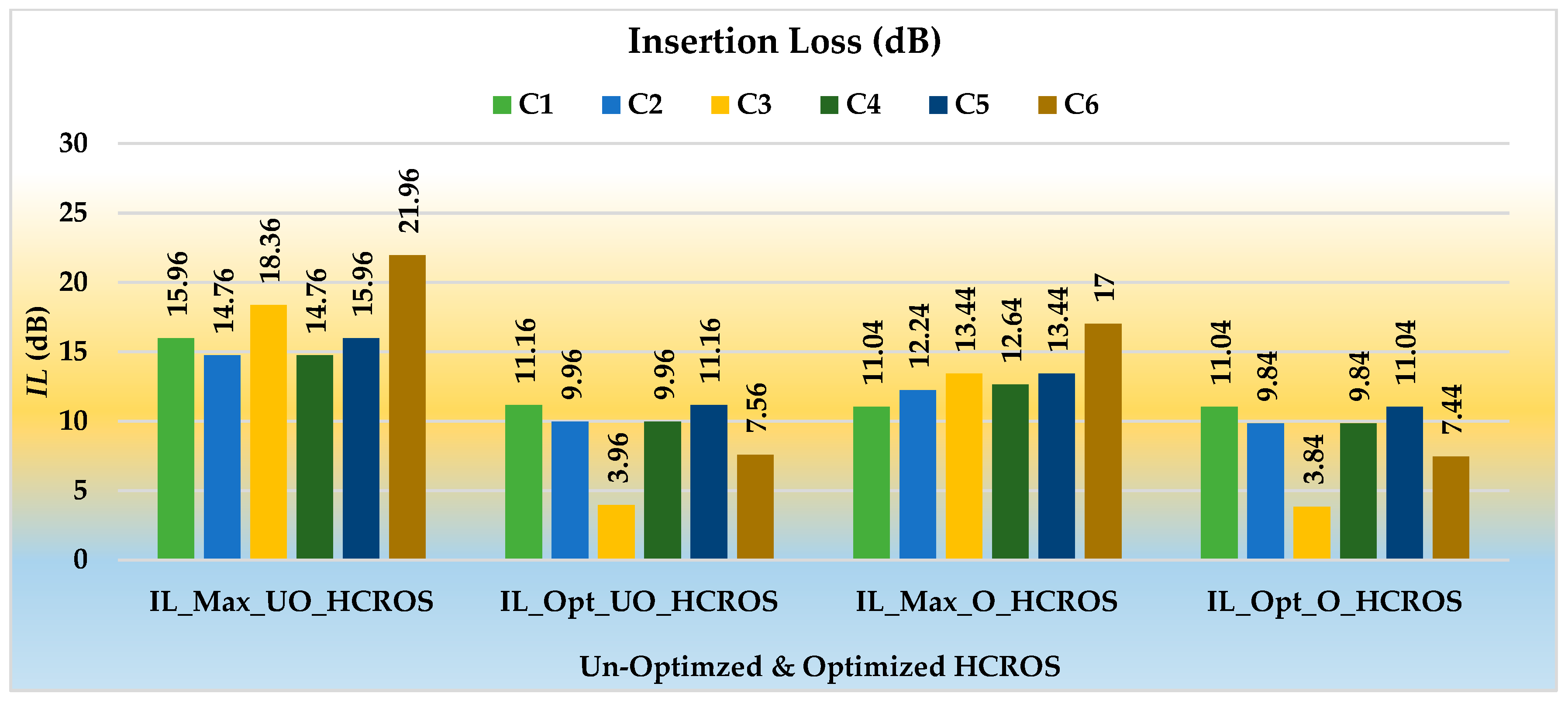
| Insertion Loss (dB) | Maximum/Minimum | Maximum (ILMax_UO_HCROS) | Optimal (ILOpt_UO_HCROS) | Maximum (ILMax_O_HCROS) | Optimal (ILOpt_O_HCROS) |
| Max. IL | 21.96 | 12.36 | 18.24 | 12.24 | |
| Min. IL | 11.16 | 3.96 | 7.44 | 3.84 | |
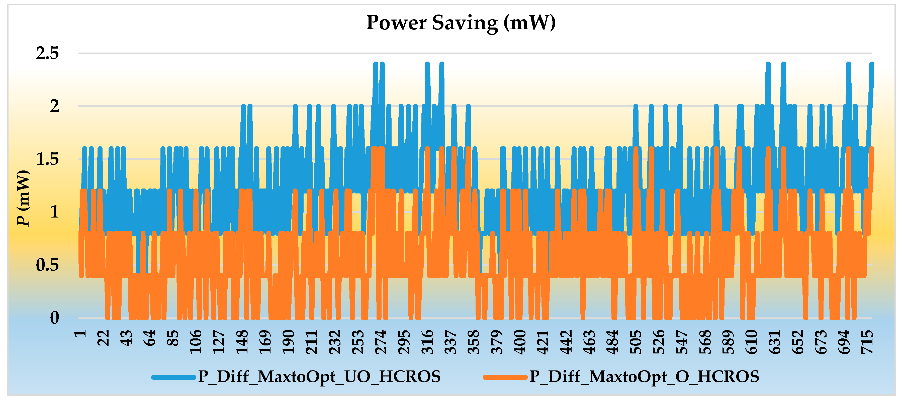
| Power Saving (mW) | Maximum/Minimum | Difference (PDiff_MaxtoOpt_UO_HCROS) | Difference (PDiff_MaxtoOpt_O_HCROS) | ||
| Max. Power Saving | 2.4 | 1.6 | |||
| Min. Power Saving | 0.4 | 0 | |||
| Insertion Loss Reduction (dB) | Maximum/Minimum | Difference (ILDiff_MaxtoOpt_UO_HCROS) | Difference (ILDiff_MaxtoOpt_O_HCROS) | ||
| Max. IL Reduction | 14.4 | 9.6 | |||
| Min. IL Reduction | 2.4 | 0 | |||
© 2019 by the authors. Licensee MDPI, Basel, Switzerland. This article is an open access article distributed under the terms and conditions of the Creative Commons Attribution (CC BY) license (http://creativecommons.org/licenses/by/4.0/).
Share and Cite
Yahya, M.R.; Wu, N.; Yan, G.; Ahmed, T.; Zhang, J.; Zhang, Y. HoneyComb ROS: A 6 × 6 Non-Blocking Optical Switch with Optimized Reconfiguration for ONoCs. Electronics 2019, 8, 844. https://doi.org/10.3390/electronics8080844
Yahya MR, Wu N, Yan G, Ahmed T, Zhang J, Zhang Y. HoneyComb ROS: A 6 × 6 Non-Blocking Optical Switch with Optimized Reconfiguration for ONoCs. Electronics. 2019; 8(8):844. https://doi.org/10.3390/electronics8080844
Chicago/Turabian StyleYahya, Muhammad Rehan, Ning Wu, Gaizhen Yan, Tanveer Ahmed, Jinbao Zhang, and Yuanyuan Zhang. 2019. "HoneyComb ROS: A 6 × 6 Non-Blocking Optical Switch with Optimized Reconfiguration for ONoCs" Electronics 8, no. 8: 844. https://doi.org/10.3390/electronics8080844
APA StyleYahya, M. R., Wu, N., Yan, G., Ahmed, T., Zhang, J., & Zhang, Y. (2019). HoneyComb ROS: A 6 × 6 Non-Blocking Optical Switch with Optimized Reconfiguration for ONoCs. Electronics, 8(8), 844. https://doi.org/10.3390/electronics8080844