Article

Enhanced Photoresponsivity of All-Inorganic (CsPbBr3) Perovskite Nanosheets Photodetector with Carbon Nanodots (CDs)

1
Nanobio Device Laboratory, School of Electrical and Electronic Engineering, Yonsei University, Seoul 120-749, Korea
2
Inter-university Semiconductor Research Center (ISRC) and the Department of Electrical and Computer Engineering, Seoul National University, Seoul 151-744, Korea
3
Biomaterials Laboratory, Department of Chemical and Biomolecular Engineering, Yonsei University, Seoul 120-749, Korea
*
Author to whom correspondence should be addressed.
Electronics 2019, 8(6), 678; https://doi.org/10.3390/electronics8060678
Submission received: 23 May 2019 / Revised: 12 June 2019 / Accepted: 13 June 2019 / Published: 14 June 2019
(This article belongs to the Special Issue Advanced Technologies in Nanoelectronics)

Abstract

:
A hybrid composite photodetector based on cesium lead bromine perovskite (CsPbBr3) nanosheets and carbon nanodots (CDs) was fabricated on a quartz substrate by a one-step method of spin-coating and hot-plate annealing. The responsivity of the CsPbBr3/CD hybrid composite photodetector was 608 mAW−1 (under a 520-nm laser diode source applied at 0.2 mWcm−2), almost three times higher than that of a CsPbBr3-based photodetector (221 mAW−1). The enhanced performance of the CsPbBr3/CD photodetector is attributable to the high band alignment of the CDs and CsPbBr3, which significantly improves the charge extraction at the CsPbBr3/CD interface. Moreover, the hybrid CsPbBr3/CD photodetector exhibited a fast response time with a rise and decay time of 1.55 and 1.77 ms, which was faster than that of a pure CsPbBr3 based photodetector, indicating that the CDs accelerate the extraction of electrons and holes trapped in the CsPbBr3 film.

Graphical Abstract

1. Introduction

Organic–inorganic halide perovskites have shown high performance in photodetectors [1,2,3,4,5], owing to their outstanding electrical and optical properties, including tunable bandgap [6], strong optical absorption [7], long carrier diffusion length [8], large carrier mobilities [9], and low deep state defects [10]. Moreover, they can be fabricated by low-cost, low-temperature solution-processing techniques such as drop-casting [11], spray-coating [12], spin-coating [13], and doctor-blading [14]. Accordingly, they are future candidate materials for low-cost, facile, flexible, and large-scale printable photodetectors [2,15]. Among the organolead halide perovskites, all-inorganic lead halide perovskites CsPbX3 (X = I, Br, Cl) are recognized for their high stability in humid environments (unlike organic–inorganic halide perovskites), high absorption coefficient (2 × 105 cm−1) [16], and large carrier mobility (1000 cm2 V−1S−1) [17]. With these outstanding electrical and optical properties, photodetectors based on all-inorganic lead halide perovskites should strongly outperform devices based on organic–inorganic halide perovskites or 2D MoS2, reaching the performance of silicon-based devices [18,19]. However, the actual performance of solution-processed photodetectors based on all-inorganic perovskite film has been unsatisfactory, exceeded not only by devices based on 2D MoS2 or silicon, but also by photodetectors based on organic–inorganic hybrid perovskites [20,21,22]. Later, this poor performance was linked to the low conductivity of solution-assembled film resulting from poor continuity of the film, which inevitably creates interfacial traps that lower the carrier extraction and transport efficiency [19]. The performance can be enhanced by fabricating bilayer heterostructure photodetectors, in which the perovskite layer (which absorbs the light) is combined with another functional material such as graphene or a 2D material (which transports the photocarriers). A hybrid phototransistor based on graphene–CsPbBr3−xIx perovskite nanocrystals achieved a high photo-responsivity of 108 A W−1 and a detectivity of 1016 Jones under 405-nm illumination at 0.07 mW−2 [23]. Song et al. [24], fabricated a hybrid photodetector based on 2D MoS2 and CsPbBr3 nanosheets, which exhibited high photoresponsivity (4.4 AW−1), an external quantum efficiency of 302%, and a detectivity of 2.5 × 10¹⁰ Jones. Although these devices achieved excellent performance, the transfer method of the graphene and 2D Mos2 (mechanical exfoliation) is complicated and expensive, and hence inappropriate for flexible and large-area fabrication.
Carbon nanodots (CDs) (novel nano-sized carbon structures) have also demonstrated excellent performance in applications such as photocatalysis [25], bioimaging [26], and supercapacitors [27]. CDs are favored for their excellent photoluminescence [28], low toxicity [29], biocompatibility [30], simple synthesis [31], and high stability [32]. In optical and optoelectronic applications, CDs have been mainly exploited in light-emitting diodes [33,34,35]. They also boost the performance of optical devices by providing an electron transportation layer. Xie et al. [36] reported a core shell heterojunction photovoltaic device composed of a silicon nanowire array and carbon quantum dots, which reached a power conversion efficiency of 9.10% under AM1.5G irradiation. Guo et al. [37], fabricated a photodetector based on zinc oxide quantum dots and CDs, which achieved a detectivity and noise equivalent power of 3.1 × 10¹⁷ cmHz1/2/W and 7.8 × 10⁻²⁰ W, respectively. Moreover, in photosensing applications, it has been demonstrated that the photoresponsivity of p–n junction based photodetectors can be increased by the use of graphene nanosheets composites [38,39]. Dai et al. [40], demonstrated transparent and flexible (TFT) based on solution processed-graphene nanosheets and amorphous indium–gallium–zinc-oxide (a-IGZO) composites, with an achieved mobility of 23.8 (cm2 V−1 s−1), which is about thirty times higher than that of the pristine a-IGZO TFTs (0.82 cm2 V−1 s−1). However, to our knowledge, composites of CDs and all-inorganic perovskites in photosensing applications have been scarcely reported. Fang et al. [41] demonstrated an enhanced efficiency (17.62%) in mesoscopic perovskite solar cells after incorporating graphene quantum dots (GQDs) into CH3NH3PbI3. The improvement was attributed to the high conductivity of the GQDs, which facilitate electron extraction from the perovskite, and effectively restrict the electron traps at the perovskite grain boundaries. It has also been reported that perovskite materials have many defects at the surface or in the grain boundaries, which can introduce local trap states [41]. During device operation photogenerated carriers can be absorbed in these trap states. Carbon dots can passivate these trap states due to their surface and edge effects. Therefore, compared to other carbon materials, carbon dot/inorganic perovskite composite layers have advantages over other materials due to their better stability under thermal and humid conditions. In addition, compared to the bilayer perovskite photodetectors mentioned above, single layer composite perovskite photodetectors have potential advantages in production due to their simple and cheap fabrication design. Thus, it is believed that excellent photo-generation characteristics of perovskite material and carrier transport properties of carbon dots make a good combination for a single layer, cost effective, visible range photodetector.
In this work, we fabricate a solution-processed hybrid photodetector based on all-inorganic cesium lead bromine (CsPbBr3) perovskite nanosheets and CDs. The CDs are combined with perovskite to enhance the transport and separation of the photogenerated carriers in the perovskite. Here we exploit the excellent alignment of CDs with the perovskites, which restricts the recombination rate of the photogenerated carriers and enhances the photocurrent over the CsPbBr3 device without CDs. We demonstrate the higher performance of the hybrid CsPbBr3/CD composite photodetector (with an on/off ratio of 102 and a responsivity of 608 mAW−1) than the CD-free perovskite-based photodetector (with a responsivity of 221 mAW−1).

2. Materials and Methods

Starting materials: All materials were purchased from Aladdin (Shanghai, china) and Sigma Aldrich (Seoul, Korea) and used without further purification.
Preparation of perovskite nanosheets: The CsPbBr3 nanosheets were synthesized by the method in Song [24]. First, CsBr and PbBr2 (molar ratio 1:0.5) were dissolved by ultrasonication in 15 mL of dimethyl sulfoxide for 1 h, yielding a mixed solution. Second, 0.2 mL of the as-prepared solution was dropped into 1 mL octadecylamine and acetic acid solution (50 mg/mL) and magnetically stirred for 2 min. Then, 15 mL of toluene was injected into this solution. After a few minutes, the solution was centrifuged, and the collected precipitate was redispersed in toluene and centrifuged once more. Finally, the precipitate was dispersed in 4 mL of toluene to form 2 mg/mL perovskite solution.
Preparation of carbon nanodots: The carbon nanodots (CDs) were prepared by the method in Barman [42]. First, an aqueous solution was prepared by mixing 0.1 g of branched polyethylenimine with 10 mL of hot water. After adding 0.1 g citric acid and stirring the solution for 1 h, we transferred the prepared solution to an autoclave and heated it at 230 °C for 5 h. The solution was cooled to room temperature, centrifuged, and purified by dialysis. Finally, the CDs were collected from the solution after drying for 24 h at 75 °C in a high vacuum, and frozen for further use.
Preparation of CsPbBr3/CD composite solution: The dried CDs were dispersed in 2 mL of ethanol to form a 4 mg/mL CD solution. The CsPbBr3/CD composite solution was then prepared by mixing the perovskite nanosheets and CD solutions at a volume ratio of 1:0.25. The composite solution was stirred for 12 h and used without further modification.
Characterization of materials: The crystal structures and morphologies of the products were analyzed by transmission electron microscopy (TEM, JEM-F200, Tokyo, Japan), field-emission scanning electron microscopy (SEM, JEOL-7800F, Tokyo, Japan), and atomic force microscopy (AFM, NX-10-Park Systems). The X-ray diffraction (XRD, Ultima IV, Rigaku, Tokyo, Japan) patterns were obtained by a diffractometer (Ultima IV; Rigaku). The optical spectra were characterized by a photoluminescence (PL) spectrophotometer (OPTIZEN 3220UV, Agilent Technologies Inc., USA) and an ultraviolet–visible light (UV–vis) spectrophotometer (JASCO V-650, JASCO Deutschland GmbH, Pfungstadt, Germany).
Device fabrication process: A quartz substrate (SK-1300 series, 2.5 × 2.5 cm2, OHAIR Quartz Co. Ltd., Seoul, Korea) was ultrasonically cleaned with acetone and isopropanol, then rinsed with deionized water and dried under an N2 flow. Subsequently, the substrate was treated by O2 plasma for 15 min, and the Cr/Au (4/80 nm) electrodes were fabricated by standard lithography, thermal evaporation, and the wet etching process. The channel length and width of the electrodes were 20 and 1000 µm, respectively. The composite solution was then spin coated on the treated substrate at 2000 rpm for 10 s and annealed at 100 °C for 15 min.
Device performance measurements: The photoelectric current–voltage (I–V) characteristics were obtained by a measurement system equipped with a Keithley 4200 SCS parameter analyzer, and a 520-nm laser diode as the light source (MDL-III-520L, Changchun New Industries Optoelectronics Technology Co. Ltd., Changchun, China). The current–time (I–t) characteristics were obtained under the same laser diode source and a Keithley 4200 SCS with an optical chopper (SRS, SR540) at 1 Hz. The response time was measured under the same laser diode source, optical chopper (f = 100 Hz), and an oscilloscope (model TDS3012, Tektronix).

3. Results and Discussion

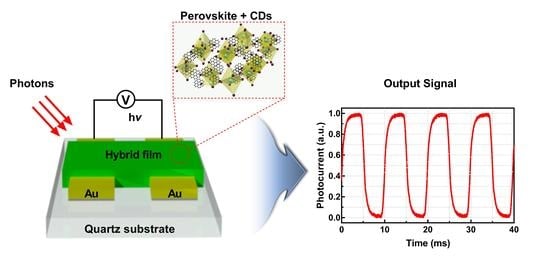
3.1. Device Structure

Figure 1 illustrates the structure of the CsPbBr3/CD hybrid composite photodetector fabricated on the quartz substrate. Initially, Cr/Au (4 nm/80 nm) were thermally deposited on the quartz substrate by standard lithography, thermal evaporation, and wet etching, yielding electrodes with a total effective area of 2 × 10⁻⁴ cm2 (Figure S1). The left image in Figure 1 shows the emission colors of the CsPbBr3 and CD solutions under white light. The CsPbBr3 solution emitted typically yellow light while the CD solution showed a watery emission [22,42,43]. The right image in Figure 1 is a schematic of the composite materials containing mixed perovskite nanosheets and CDs. The small square shows the unit cells of CsPbBr3 and the CDs. The unit cell of perovskite nanosheets is typically a cubic structure formed by Pb and Br bonded to both Cs atoms [44]. In contrast, the carbon nanodots form a spherical graphitic-like structure [45]. The CsPbBr3/CD composite film on glass was almost 200 nm thick (as verified by a step profiler) and was both compact and uniform (Figure S2). It is also worth mentioning that the film thickness of the CsPbBr3/CD composite film (200 nm) was actually thinner than that of the pure CsPbBr3 film (228 nm), which indicated that the thickness of composite film was slightly reduced when the carbon nanodots were incorporated [46]. This could have resulted from viscosity changes of the composite solution after the addition of the carbon nanodots. However, as discussed later in this section, the morphology of the CsPbBr3 and CsPbBr3/CD composite film was analyzed to point out the role of the CDs.

3.2. Characterization of CDs, CsPbBr3, and CsPbBr3/CD Composite Solutions

The crystal structures and qualities of the CDs, CsPbBr3, and CsPbBr3/CD were determined from the low-magnification and high-resolution (HR) TEM images and from Fourier transform images (see Figure 2). The CDs were narrowly distributed in size, with an average diameter of ~4.5 nm (Figure 2a). The lattice fringes (0.21 nm) of the CD structure are clearly seen in Figure 2b (see also Figure S3a), and the fast Fourier transform image of the selected area (enclosed by the dashed red circle in Figure 2b) revealed the high crystallinity of the CDs [43,45]. TEM and HRTEM images of the CsPbBr3 nanosheets are shown in Figure 2d,e, respectively (see also Figure S3b). These images clarified the cubic structure of the perovskite nanosheets, with a lattice fringe of approximately 0.58 nm [22]. Moreover, the Fourier transform image in Figure 2f confirmed the crystalline structure of perovskite. Meanwhile, in the TEM image of the sample combining the CDs with the CsPbBr3 nanosheet solution, evidence of both materials was expected. The presence of both materials was indeed confirmed in TEM images of the composite sample (Figure 2g,h,k). Carbon nanodots (dashed red circles) and perovskite nanosheets (green-lined square) are clearly shown in Figure 2k. Moreover, to clarify that these nanodots were CDs alone, we magnified their structure, as seen in Figure S3c,d. These images clearly reveal the hexagonal honeycomb structure of graphite [45].
The CsPbBr3 and CsPbBr3/CD composite films were further characterized by their powder XRD patterns. The XRD spectra are displayed in Figure 3. The peaks in the spectra of the CsPbBr3 film, labeled 100, 110, 200, 210, 211, and 220, corresponded to the cubic crystalline structure of CsPbBr3 nanosheets as reported elsewhere [22]. However, the peaks in the XRD spectra of the CsPbBr3/CD corresponded only to the cubic structure of CsPbBr3; the characteristic CD peaks were absent. According to the literature, the XRD patterns of CDs exhibit one peak between 2θ = 20° and 2θ = 30° (depending on the size, structure, and synthesis process of the CDs) [47]. The discrepancy might be attributable to coverage of the 4.5 nm-diameter CDs by the considerably larger perovskite nanosheets, which might have dominated the XRD detection. Supporting this idea, the XRD pattern of perovskite and carbon nanotube composite film in a previous study showed only the peaks of the perovskite structure [48].

3.3. Optical characterization of the CDs, CsPbBr3, and CsPbBr3/CD Composite Solutions

The optical properties of the CDs, CsPbBr3, and CsPbBr3/CD composite solutions were characterized by their UV–vis spectra. As shown in Figure 4a, the solution of pure CDs absorbed in the deep-to-near UV region with a peak near 405 nm, corresponding to a bandgap of 3.61 eV [42,43]. In contrast, the CsPbBr3 solution absorbed wavelengths from the UV to the visible region with an absorption peak at 520 nm, corresponding to a bandgap of 2.4 eV [22,24]. The absorption spectrum of the CsPbBr3/CD composite solution displayed the same characteristics as that of pure CsPbBr3 solution, corresponding to the same bandgap. This result indicated that photon absorption by the composite film was dominated by perovskite. Moreover, the absorption intensity was lower in the CsPbBr3/CD composite solution than in pure CsPbBr3 solution. This was confirmed by naked-eye observation under white and UV (365-nm) light: the CsPbBr3/CD composite solution was lighter in color than the pure CsPbBr3 solution (see insets of panels (a) and (b) of Figure 4, respectively).
The PL spectrometer is a powerful optical analyzer of the charge transfer and recombination processes in composite materials [49]. The PL spectra of the pure CDs, pure CsPbBr3, and composite CsPbBr3/CD solutions are presented in Figure 4b. The PL intensities of the pure CDs and CsPbBr3 solutions peaked near the bandgap peaks. The higher intensity of the CsPbBr3 peak than the CD peak indicated a higher recombination rate in perovskite than in pure CDs. However, the PL spectrum of the CsPbBr3/CD composite solution peaked at a similar wavelength to the CsPbBr3 solution, revealing that perovskite dominated the emission process in the composite solution. Nevertheless, the PL intensity was almost one order of magnitude lower in the composite solution than in pure CsPbBr3, indicating a considerable amount of charge transfer at the CsPbBr3/CD interface. In other words, the carbon nanotubes reduced the recombination rate of photogenerated carriers in the CsPbBr3/CD, improving the light-absorbance performance over that of pure perovskite in photosensing applications (as demonstrated later in this work). To understand the charge transfer across the CsPbBr3/CD interface, we present the energy-band structures of the perovskite and CD materials in Figure 4c. This diagram shows the valance band maximum (VBM) and conduction band minimum (CBM) with respect to the vacuum level. The VBMs and CBMs of perovskite and CDs were obtained from Song et al. [24] and Barman et al. [42], respectively. The hybrid composite system showed a type-II band alignment with CBM and VBM offsets of 0.22 and 1.43 eV, respectively, from those of CsPbBr3 perovskite and pure CDs. This type of band alignment suggested that the photogenerated electrons in perovskite moved into the CDs, while the photogenerated holes in perovskite were localized within the perovskite (owing to the raised CDM of the CDs). This analysis consolidated the PL spectra shown in Figure 4b, which hinted that the recombination rate was lower in the hybrid composite than in pure perovskite solution. To understand how the hybrid composite limited the recombination rate, we hypothesized the recombination mechanism in pure CsPbBr3 and the CsPbBr3/CD hybrid composite (see Figure 4d). When pure CsPbBr3 absorbed photons with sufficient energy (similar to or greater than its own bandgap), electron–hole pairs were photogenerated in the perovskite, and the electrons moved from the valance to the conduction band, leaving empty spaces for the holes (absorption phenomenon). Within one picosecond, the conduction-band electrons relaxed and finally recombined with the holes in the valence band (the band-to-band recombination process) [46]. However, in the CsPbBr3/CD hybrid composite, the recombination process was reduced because the electrons moved to the CDs while the holes localized within the perovskite, thus reducing the recombination probability.

3.4. Performances of Photodetectors Based on CsPbBr3 and CsPbBr3/CD Composite Film

The performance of a photodetector based on the CsPbBr3/CD hybrid composite film was compared with that of a photodetector based on pure CsPbBr3. The photoelectrical measurements were performed under a 520-nm laser diode with a light intensity of 0.2 mWcm−2. The I–V characteristics of the pure CsPbBr3 and CsPbBr3/CD hybrid composite photodetectors are shown in Figure 5a,b, respectively. It can be observed that the IV curves for the pure CsPbBr3 and CsPbBr3/CD hybrid composite photodetectors is symmetrical since the photocurrent value of each device (at –10 V and 10 V) were almost the same [24]. The dark currents of the photodetectors based on pure CsPbBr3 and the CsPbBr3/CD composite film were 0.09 and 0.12 nA under a 10-V bias voltage, respectively. This result was expected, as the CDs in the perovskite increased the conductivity of the hybrid photodetector. Similarly, under irradiation with 520-nm laser light at 0.2 mWcm−2, the photocurrent of the CsPbBr3/CD hybrid composite photodetector was 24.46 nA (versus 9 nA in the CsPbBr3-based photodetector). To further confirm the photocurrent enhancement in the hybrid composite device, we obtained the I–t curves by irradiating both devices with positive signals generated from the same 520-nm light source and a 1-Hz optical chopper [50]. The I–t curves of both devices are presented in Figure 5c. Under the illumination conditions (0.2 mWcm−2), the photocurrents of the pure CsPbBr3–based and hybrid composite-based devices sharply increased when the bias voltage (10 V) was applied, reflecting the increase in carrier drift velocity. When the laser was turned off, the photocurrents sharply fell to their initial values. The devices promptly generated a photocurrent with a reproducible response in the on–off cycles. In addition, the photocurrent was higher in the hybrid device than in the pure device, and both currents were similar to those measured in the I–V curves under the same applied voltage. The response, rise, and decay times of the hybrid composite devices are illustrated in Figure 5d,e,f, respectively. The rise and decay times are the times required for the photocurrent to reach 90% of its peak value and decay to 10% of its peak value, respectively [51]. The hybrid photodetector exhibited a rise and decay time of 1.55 and 1.77 ms, respectively. The hybrid device not only showed a faster response time compared with that of the pure CsPbBr3 nanosheets (65.2 and 18.5 ms) reported by Song et al. [24], but also better than those of devices based on all-inorganic micro-particles [52] and nanorods [53]. This result confirmed two roles for the CDs in the hybrid composite device: enhancing the conductivity of the composite film, and accelerating the electron extraction. To realize the effect of the CDs on the device performance, we determined the on/off ratio (photocurrent to dark/current ratio) and the responsivity R (electrical output per optical input) of the pure CsPbBr3 and CsPbBr3/CD hybrid composite photodetectors by Equations (1) and (2), respectively [54]:
I O N / O F F = I L i g h t I d a r k ,
R = I L i g h t I d a r k P   O p t i c a l × A .
In these expressions, Ilight and Idark are the dark current and photocurrent of the device, respectively, POptical is the light power intensity, and A is the effective illuminated area of the device. The on/off ratio of the CsPbBr3/CD composite photodetector was almost double that of the CsPbBr3 photodetector (217 vs. 102). Meanwhile, the R of the CsPbBr3/CD composite device was 0.61 AW−1, almost three times that of the CD-free CsPbBr3 photodetector (0.22 AW−1). Table 1 compares the responsivities of the CsPbBr3/CD hybrid composite photodetector and other reported devices. The proposed hybrid photodetector outperformed the previous devices based on CsPbBr3 nanosheets, quantum dots, and micro-particles. To further understand the role of the carbon nanodots in the performance enhancement of the all-inorganic perovskites, we analyzed the morphology of the CsPbBr3 and CsPbBr3/CD composite films using the AFM and SEM, as shown in Figures S4–S7. The top-surface SEM and AFM images of CsPbBr3 film revealed that the film had a high surface roughness with many defects, which resulted in poor performance (low conductivity) [19]. Moreover, when the CDs were blinded with the perovskite, the surface roughness of CsPbBr3/CD composite film was reduced and became more continues with fewer defects (Figure S8). As a result, the performance of the photodetector based on CsPbBr3/CD composite film was higher than that of the pure perovskite based photodetector.

3.5. Working Principle of the CsPbBr3/CD Composite Photodetector

The working mechanism of the composite photodetector can be explained by the energy-band structures of CsPbBr3 and the CDs, as seen in Figure 4c, which revealed a type-II band alignment at the interface. Under a light source with energy equal to or greater than the bandgap energy of the composite (i.e., ≥2.4 eV) [24], the CsPbBr3 absorbed photons, and the electrons in its valance band moved up to the conduction band, leaving their empty spaces as holes. The electrons in the conduction band of perovskite then moved downward into the conduction band of the CDs, because the CDs have higher electron affinity (a lower conduction band) than perovskite. Meanwhile, the holes remained in the valance band of perovskite because perovskite has a lower ionization potential (a higher valance band) than the CDs [24,37,46]. This type-II band alignment efficiently enhanced the charge separation at the CsPbBr3/CD interface, enhancing both the photocurrent and responsivity of the photodetector.

4. Conclusions

We fabricated a solution-processed hybrid photodetector based on perovskite (CsPbBr3) nanosheets and carbon nanodot (CD) composite film. The composite film was prepared by mixing solutions of perovskite nanosheets (2 mg/mL) and CDs (4 mg/mL) at a volume ratio of 1:0.25. As revealed in the photoluminescence spectra, the CDs limited the recombination rate in the hybrid CsPbBr3/CD composite film by significantly enhancing the charge extraction at the CsPbBr3/CD interface. Moreover, the photoelectrical measurements confirmed a photocurrent of 24.46 nA in the CsPbBr3/CD composite (versus 9 nA in the CsPbBr3-based device), whereas the dark current was increased only to 0.11 nA (from 0.09 nA in the CsPbBr3-based device). Consequently, the responsivity of the CsPbBr3/CD hybrid composite photodetector was almost three times that of the CD-free CsPbBr3 photodetector (608 mAW−1 vs. 221 mAW−1).

Supplementary Materials

The following are available online at https://www.mdpi.com/2079-9292/8/6/678/s1: Figure S1. Optical image of the device structure with a channel length and width of 20 and 1000 µm, respectively; Figure S2. Cross-sectional SEM image of the device structure showing thickness of composite film; Figure S3. HRTEM images of typical (a) CDs, (b) perovskite, and (c), (d) CsPbBr3/CD composite showing the hexagonal honeycomb structure of the CDs; Figure S4. Top-surface SEM image of the CsPbBr3 and the CsPbBr3/CD films in (a) and (b), respectively; Figure S5. 2DAFM image of the CsPbBr3 film along with line profile of red line in (a) and (b), 3D AFM image of the CsPbBr3 film (c); Figure S6. 2DAFM image of the CsPbBr3/CD film along with line profile of green line in (a) and red line in (b), 3D AFM image of the CsPbBr3/CD film (c); Figure S7. 3D AFM image of the CsPbBr3/CD film showing defects on the surface of the film; Figure S8. Optical image of device channel after depositing the CsPbBr3/CD.

Author Contributions

Conceptualization, H.A. and C.M.; Resources, J.W., M.L., and M.K.; Writing—original draft, H.A.; Writing—review and editing, T.L.

Funding

This work was financially supported by the National Research Foundation (NRF) of Korea (Grant NRF-2017M3A7B4049466 and NRF-2017K2A9A2A06013377). Also it was supported by Priority Research Centers Program through the National Research Foundation of Korea (NRF-2019R1A6A1A11055660).

Conflicts of Interest

The authors declare no conflict of interest.

References

  1. Deng, H.; Yang, X.; Dong, D.; Li, B.; Yang, D.; Yuan, S.; Qiao, K.; Cheng, Y.B.; Tang, J.; Song, H. Flexible and semitransparent organolead triiodide perovskite network photodetector arrays with high stability. Nano Lett. 2015, 15, 7963–7969. [Google Scholar] [CrossRef] [PubMed]
  2. Hu, X.; Zhang, X.; Liang, L.; Bao, J.; Li, S.; Yang, W.; Xie, Y. High-Performance Flexible Broadband Photodetector Based on Organolead Halide Perovskite. Adv. Funct. Mater. 2014, 24, 7373–7380. [Google Scholar] [CrossRef]
  3. Horváth, E.; Spina, M.; Szekrényes, Z.; Kamarás, K.; Gaal, R.; Gachet, D.; Forró, L. Nanowires of Methylammonium Lead Iodide (CH3NH3PbI3) prepared by low temperature solution-mediated crystallization. Nano Lett. 2014, 14, 6761–6766. [Google Scholar] [CrossRef] [PubMed]
  4. Jang, D.M.; Kim, D.H.; Park, K.; Park, J.; Lee, J.W.; Song, J.K. Ultrasound synthesis of lead halide perovskite nanocrystals. J. Mater. Chem. C 2016, 4, 10625–10629. [Google Scholar] [CrossRef]
  5. Jang, D.M.; Park, K.; Kim, D.H.; Park, J.; Shojaei, F.; Kang, H.S.; Ahn, J.-P.; Lee, J.W.; Song, J.K. Reversible Halide Exchange Reaction of Organometal Trihalide Perovskite Colloidal Nanocrystals for Full-Range Band Gap Tuning. Nano Lett. 2015, 15, 5191–5199. [Google Scholar] [CrossRef] [PubMed]
  6. Zhang, F.; Zhong, H.; Chen, C.; Wu, X.; Hu, X.; Huang, H.; Han, J.; Zou, B.; Dong, Y. Brightly Luminescent and Color-Tunable Colloidal CH3NH3PbX3 (X = Br, I, Cl) Quantum Dots: Potential Alternatives for Display Technology. ACS Nano 2015, 9, 4533–4542. [Google Scholar] [CrossRef]
  7. Adinolfi, V.; Peng, W.; Walters, G.; Bakr, O.M.; Sargent, E.H. The Electrical and Optical Properties of Organometal Halide Perovskites Relevant to Optoelectronic Performance. Adv. Mater. 2018, 30, 1–13. [Google Scholar] [CrossRef]
  8. Dong, Q.; Fang, Y.; Shao, Y.; Mulligan, P.; Qiu, J.; Cao, L.; Huang, J. Electron-hole diffusion lengths > 175 μm in solution-grown CH3NH3PbI3 single crystals. Science 2015, 347, 967–970. [Google Scholar] [CrossRef]
  9. Wehrenfennig, C.; Eperon, G.E.; Johnston, M.B.; Snaith, H.J.; Herz, L.M. High charge carrier mobilities and lifetimes in organolead trihalide perovskites. Adv. Mater. 2014, 26, 1584–1589. [Google Scholar] [CrossRef]
  10. Yang, W.S.; Park, B.-W.; Jung, E.H.; Jeon, N.J. Iodide management in formamidinium-lead-halide–based perovskite layers for efficient solar cells. Science 2017, 356, 1376–1379. [Google Scholar] [CrossRef]
  11. Kamminga, M.E.; Fang, H.-H.; Loi, M.A.; ten Brink, G.H.; Blake, G.R.; Palstra, T.T.M.; ten Elshof, J.E. Micropatterned 2D hybrid perovskite thin films with enhanced photoluminescence lifetimes. ACS Appl. Mater. Interfaces 2018, 10, 12878–12885. [Google Scholar] [CrossRef] [PubMed]
  12. Bishop, J.E.; Mohamad, D.K.; Wong-Stringer, M.; Smith, A.; Lidzey, D.G. Spray-cast multilayer perovskite solar cells with an active-area of 1.5 cm2. Sci. Rep. 2017, 7, 7962. [Google Scholar] [CrossRef] [PubMed]
  13. Zhao, F.; Xu, K.; Luo, X.; Lv, W.; Peng, Y.; Wang, Y.; Lu, F.; Xu, S. Ultrasensitivity broadband photodetectors based on perovskite: Research on film crystallization and electrode optimization. Org. Electron. Phys. Mater. Appl. 2017, 46, 35–43. [Google Scholar] [CrossRef]
  14. Li, S.; Tong, S.; Yang, J.; Xia, H.; Zhang, C.; Zhang, C.; Shen, J.; Xiao, S.; He, J.; Gao, Y.; et al. High-performance formamidinium-based perovskite photodetectors fabricated via doctor-blading deposition in ambient condition. Org. Electron. Phys. Mater. Appl. 2017, 47, 102–107. [Google Scholar] [CrossRef]
  15. Deng, W.; Zhang, X.; Huang, L.; Xu, X.; Wang, L.; Wang, J.; Shang, Q.; Lee, S.-T.; Jie, J. Aligned Single-Crystalline Perovskite Microwire Arrays for High-Performance Flexible Image Sensors with Long-Term Stability. Adv. Mater. 2016, 28, 2201–2208. [Google Scholar] [CrossRef] [PubMed]
  16. Yettapu, G.R.; Talukdar, D.; Sarkar, S.; Swarnkar, A.; Nag, A.; Ghosh, P.; Mandal, P. Terahertz Conductivity within Colloidal CsPbBr3 Perovskite Nanocrystals: Remarkably High Carrier Mobilities and Large Diffusion Lengths. Nano Lett. 2016, 16, 4838–4848. [Google Scholar] [CrossRef] [PubMed]
  17. De Roo, J.; Ibáñez, M.; Geiregat, P.; Nedelcu, G.; Walravens, W.; Maes, J.; Martins, J.C.; Van Driessche, I.; Kovalenko, M.V.; Hens, Z. Highly Dynamic Ligand Binding and Light Absorption Coefficient of Cesium Lead Bromide Perovskite Nanocrystals. ACS Nano 2016, 10, 2071–2081. [Google Scholar] [CrossRef] [PubMed] [Green Version]
  18. Liu, H.; Zhang, X.; Zhang, L.; Yin, Z.; Wang, D.; Meng, J.; Jiang, Q.; Wang, Y.; You, J. A high-performance photodetector based on an inorganic perovskite-ZnO heterostructure. J. Mater. Chem. C 2017, 5, 6115–6122. [Google Scholar] [CrossRef]
  19. Li, X.; Yu, D.; Chen, J.; Wang, Y.; Cao, F.; Wei, Y.; Wu, Y.; Wang, L.; Zhu, Y.; Sun, Z.; et al. Constructing Fast Carrier Tracks into Flexible Perovskite Photodetectors to Greatly Improve Responsivity. ACS Nano 2017, 11, 2015–2023. [Google Scholar] [CrossRef] [PubMed]
  20. Ramasamy, P.; Lim, D.H.; Kim, B.; Lee, S.H.; Lee, M.S.; Lee, J.S. All-inorganic cesium lead halide perovskite nanocrystals for photodetector applications. Chem. Commun. 2016, 52, 2067–2070. [Google Scholar] [CrossRef]
  21. Song, J.; Xu, L.; Li, J.; Xue, J.; Dong, Y.; Li, X.; Zeng, H. Monolayer and Few-Layer All-Inorganic Perovskites as a New Family of Two-Dimensional Semiconductors for Printable Optoelectronic Devices. Adv. Mater. 2016, 4861–4869. [Google Scholar] [CrossRef] [PubMed]
  22. Gu, Y.; Dong, Y.; Song, J.; Zou, Y.; Li, X.; Zeng, H.; Li, J.; Xue, J.; Xu, L. Improving All-Inorganic Perovskite Photodetectors by Preferred Orientation and Plasmonic Effect. Small 2016, 12, 5622–5632. [Google Scholar] [CrossRef]
  23. Kwak, D.-H.; Lim, D.-H.; Ra, H.-S.; Ramasamy, P.; Lee, J.-S. High performance hybrid graphene–CsPbBr 3−x I x perovskite nanocrystal photodetector. RSC Adv. 2016, 6, 65252–65256. [Google Scholar] [CrossRef]
  24. Song, X.; Liu, X.; Yu, D.; Huo, C.; Ji, J.; Li, X.; Zhang, S.; Zou, Y.; Zhu, G.; Wang, Y.; et al. Boosting Two-Dimensional MoS2/CsPbBr3 Photodetectors via Enhanced Light Absorbance and Interfacial Carrier Separation. ACS Appl. Mater. Interfaces 2018, 10, 2801–2809. [Google Scholar] [CrossRef] [PubMed]
  25. Liu, J.; Liu, Y.; Liu, N.; Han, Y.; Zhang, X.; Huang, H.; Lifshitz, Y.; Lee, S.-T.; Zhong, J.; Kang, Z. Metal-free efficient photocatalyst for stable visible water splitting via a two-electron pathway. Science 2015, 347, 970–974. [Google Scholar] [CrossRef] [PubMed]
  26. Wei, W.; Xu, C.; Wu, L.; Wang, J.; Ren, J.; Qu, X. Non-Enzymatic-Browning-Reaction: A Versatile Route for Production of Nitrogen-Doped Carbon Dots with Tunable Multicolor Luminescent Display. Sci. Rep. 2015, 4, 3564. [Google Scholar] [CrossRef]
  27. Zhu, Y.; Ji, X.; Pan, C.; Sun, Q.; Song, W.; Fang, L.; Chen, Q.; Banks, C.E. A carbon quantum dot decorated RuO2 network: Outstanding supercapacitances under ultrafast charge and discharge. Energy Environ. Sci. 2013, 6, 3665. [Google Scholar] [CrossRef]
  28. Baker, S.N.; Baker, G.A. Luminescent Carbon Nanodots: Emergent Nanolights. Angew. Chem. Int. Ed. 2010, 49, 6726–6744. [Google Scholar] [CrossRef]
  29. Yang, S.T.; Wang, X.; Wang, H.; Lu, F.; Luo, P.G.; Cao, L.; Meziani, M.J.; Liu, J.H.; Liu, Y.; Chen, M.; et al. Carbon dots as nontoxic and high-performance fluorescence imaging agents. J. Phys. Chem. C 2009, 113, 18110–18114. [Google Scholar] [CrossRef]
  30. Qu, S.; Wang, X.; Lu, Q.; Liu, X.; Wang, L. A Biocompatible Fluorescent Ink Based on Water-Soluble Luminescent Carbon Nanodots. Angew. Chem. Int. Ed. 2012, 51, 12215–12218. [Google Scholar] [CrossRef]
  31. Wang, F.; Pang, S.; Wang, L.; Li, Q.; Kreiter, M.; Liu, C.Y. One-step synthesis of highly luminescent carbon dots in noncoordinating solvents. Chem. Mater. 2010, 22, 4528–4530. [Google Scholar] [CrossRef]
  32. Chen, Q.; Wang, Y.; Wang, Y.; Zhang, X.; Duan, D.; Fan, C. Nitrogen-doped carbon quantum dots/Ag3PO4 complex photocatalysts with enhanced visible light driven photocatalytic activity and stability. J. Colloid Interface Sci. 2017, 491, 238–245. [Google Scholar] [CrossRef]
  33. Do, S.; Kwon, W.; Rhee, S.-W. Soft-template synthesis of nitrogen-doped carbon nanodots: Tunable visible-light photoluminescence and phosphor-based light-emitting diodes. J. Mater. Chem. C 2014, 2, 4221. [Google Scholar] [CrossRef]
  34. Zhang, X.; Zhang, Y.; Wang, Y.; Kalytchuk, S.; Kershaw, S.V.; Wang, Y.; Wang, P.; Zhang, T.; Zhao, Y.; Zhang, H.; et al. Color-Switchable Electroluminescence of Carbon Dot Light-Emitting Diodes. ACS Nano 2013, 7, 11234–11241. [Google Scholar] [CrossRef] [PubMed]
  35. Wang, F.; Chen, Y.; Liu, C.; Ma, D. White light-emitting devices based on carbon dots’ electroluminescence. Chem. Commun. 2011, 47, 3502. [Google Scholar] [CrossRef]
  36. Xie, C.; Nie, B.; Zeng, L.; Liang, F.-X.; Wang, M.-Z.; Luo, L.; Feng, M.; Yu, Y.; Wu, C.-Y.; Wu, Y.; et al. Core–Shell Heterojunction of Silicon Nanowire Arrays and Carbon Quantum Dots for Photovoltaic Devices and Self-Driven Photodetectors. ACS Nano 2014, 8, 4015–4022. [Google Scholar] [CrossRef]
  37. Guo, D.-Y.; Shan, C.-X.; Qu, S.-N.; Shen, D.-Z. Highly Sensitive Ultraviolet Photodetectors Fabricated from ZnO Quantum Dots/Carbon Nanodots Hybrid Films. Sci. Rep. 2015, 4, 7469. [Google Scholar] [CrossRef]
  38. Huang, C.Y.; Chen, M.L.; Yu, C.W.; Wan, T.C.; Chen, S.H.; Chang, C.Y.; Hsu, T.Y. Dual functional photo-response for p-Si/SiO2/n-InGaZnO graphene nanocomposites photodiodes. Nanotechnology 2018, 29, 505202. [Google Scholar] [CrossRef]
  39. Huang, C.Y.; Kang, C.C.; Ma, Y.C.; Chou, Y.C.; Ye, J.H.; Huang, R.T.; Siao, C.Z.; Lin, Y.C.; Chang, Y.H.; Shen, J.L.; et al. P-GaN/n-ZnO nanorods: The use of graphene nanosheets composites to increase charge separation in self-powered visible-blind UV photodetectors. Nanotechnology 2018, 29. [Google Scholar] [CrossRef]
  40. Dai, M.K.; Lian, J.T.; Lin, T.Y.; Chen, Y.F. High-performance transparent and flexible inorganic thin film transistors: A facile integration of graphene nanosheets and amorphous InGaZnO. J. Mater. Chem. C 2013, 1, 5064–5071. [Google Scholar] [CrossRef]
  41. Fang, X.; Ding, J.; Yuan, N.; Sun, P.; Lv, M.; Ding, G.; Zhu, C. Graphene quantum dot incorporated perovskite films: Passivating grain boundaries and facilitating electron extraction. Phys. Chem. Chem. Phys. 2017, 19, 6057–6063. [Google Scholar] [CrossRef] [PubMed]
  42. Barman, M.K.; Mitra, P.; Bera, R.; Das, S.; Pramanik, A.; Parta, A. An efficient charge separation and photocurrent generation in the carbon dot-zinc oxide nanoparticle composite. Nanoscale 2017, 9, 6791–6799. [Google Scholar] [CrossRef] [PubMed]
  43. Barman, M.K.; Paramanik, B.; Bain, D.; Patra, A. Light Harvesting and White-Light Generation in a Composite of Carbon Dots and Dye-Encapsulated BSA-Protein-Capped Gold Nanoclusters. Chem. A Eur. J. 2016, 22, 11699–11705. [Google Scholar] [CrossRef] [PubMed]
  44. Chen, W.; Xin, X.; Zang, Z.; Tang, X.; Li, C.; Hu, W.; Zhou, M.; Du, J. Tunable photoluminescence of CsPbBr3perovskite quantum dots for light emitting diodes application. J. Solid State Chem. 2017, 255, 115–120. [Google Scholar] [CrossRef]
  45. Sciortino, A.; Cannizzo, A.; Messina, F. Carbon Nanodots: A Review—From the Current Understanding of the Fundamental Photophysics to the Full Control of the Optical Response. Carbon 2018, 4, 67. [Google Scholar] [CrossRef]
  46. Wang, Y.; Xia, Z.; Du, S.; Yuan, F.; Li, Z.; Li, Z.; Dai, Q.; Wang, H.; Luo, S.; Zhang, S.; et al. Solution-processed photodetectors based on organic–inorganic hybrid perovskite and nanocrystalline graphite. Nanotechnology 2016, 27, 175201. [Google Scholar] [CrossRef] [PubMed]
  47. Liu, H.; Li, Z.; Sun, Y.; Geng, X.; Hu, Y.; Meng, H.; Ge, J.; Qu, L. Synthesis of Luminescent Carbon Dots with Ultrahigh Quantum Yield and Inherent Folate Receptor-Positive Cancer Cell Targetability. Sci. Rep. 2018, 8, 1–8. [Google Scholar] [CrossRef] [PubMed] [Green Version]
  48. Ka, I.; Gerlein, L.F.; Nechache, R.; Cloutier, S.G. High-performance nanotube-enhanced perovskite photodetectors. Sci. Rep. 2017, 7, 1–8. [Google Scholar] [CrossRef] [PubMed]
  49. Shen, Y.; Yu, D.; Wang, X.; Huo, C.; Wu, Y.; Zhu, Z.; Zeng, H. Two-dimensional CsPbBr3/PCBM heterojunctions for sensitive, fast and flexible photodetectors boosted by charge transfer. Nanotechnology 2018, 29. [Google Scholar] [CrossRef]
  50. Li, Y.; Shi, Z.F.; Li, S.; Lei, L.Z.; Ji, H.F.; Wu, D.; Xu, T.T.; Tian, Y.T.; Li, X.J. High-performance perovskite photodetectors based on solution-processed all-inorganic CsPbBr3 thin films. J. Mater. Chem. C 2017, 5, 8355–8360. [Google Scholar] [CrossRef]
  51. AlZoubi, T.; Qutaish, H.; Al-Shawwa, E.; Hamzawy, S. Enhanced UV-light detection based on ZnO nanowires/graphene oxide hybrid using cost-effective low temperature hydrothermal process. Opt. Mater. 2018, 77, 226–232. [Google Scholar] [CrossRef] [Green Version]
  52. Wu, Y.; Wei, Y.; Zeng, H.; Cao, F.; Yu, D.; Li, X.; Gu, Y.; Song, J. Healing All-Inorganic Perovskite Films via Recyclable Dissolution-Recyrstallization for Compact and Smooth Carrier Channels of Optoelectronic Devices with High Stability. Adv. Funct. Mater. 2016, 26, 5903–5912. [Google Scholar] [CrossRef]
  53. Tang, X.; Zu, Z.; Shao, H.; Hu, W.; Zhou, M.; Deng, M.; Chen, W.; Zang, Z.; Zhu, T.; Xue, J. All-inorganic perovskite CsPb(Br/I)3 nanorods for optoelectronic application. Nanoscale 2016, 8, 15158–15161. [Google Scholar] [CrossRef] [PubMed]
  54. Jansen-van Vuuren, R.D.; Armin, A.; Pandey, A.K.; Burn, P.L.; Meredith, P. Organic Photodiodes: The Future of Full Color Detection and Image Sensing. Adv. Mater. 2016, 28, 4766–4802. [Google Scholar] [CrossRef] [PubMed]
  55. Ding, J.; Du, S.; Zuo, Z.; Zhao, Y.; Cui, H.; Zhan, X. High Detectivity and Rapid Response in Perovskite CsPbBr3 Single-Crystal Photodetector. J. Phys. Chem. C 2017, 121, 4917–4923. [Google Scholar] [CrossRef]
Figure 1. Schematic of the device structure and composite materials.
Electronics 08 00678 g001
Figure 2. TEM, HRTEM, and Fourier transform images of typical carbon nanodots (a), (b), (c) (top row) and CsPbBr3 (d), (e), and (f) (middle row). Bottom row shows an HRTEM image of the CsPbBr3/CD composite (g), a magnified HRTEM image of the yellow box in (g) (panel (h)), and a magnified image of the blue box in (g) (panel (k)). In (k), the dashed red circles and green-lined square outline the carbon dots and a CsPbBr3 nanosheet, respectively.
Electronics 08 00678 g002
Figure 3. X-ray powder diffraction (XRD) patterns of CsPbBr3 and CsPbBr3/CD film.
Electronics 08 00678 g003
Figure 4. Absorption spectra of CsPbBr3 and CsPbBr3/CD film (a), photoluminescence spectra of the carbon nanodots, CsPbBr3, and CsPbBr3/CD composite (b), energy-band structures of perovskite (yellow) and CDs (cyan) with green arrow representing electron transfer from conduction band of the perovskite into the conduction band of the CDs (c), and hypothesized recombination mechanisms in pure CsPbBr3 and CsPbBr3/CD composite (d). Insets in panels (a) and (b) show the colors of the solutions under white and UV light, respectively.
Electronics 08 00678 g004
Figure 5. I–V curves of (a) CsPbBr3 and (b) CsPbBr3/CD hybrid composite photodetectors under dark and illuminated (520 nm, 0.2 mWcm−1) conditions. I–t curves of CsPbBr3 and CsPbBr3/CD hybrid composite photodetectors (c), response times (d), rise times (e), and fall times (f) of the CsPbBr3/CD hybrid composite photodetector.
Electronics 08 00678 g005
Table 1. Summary of device performances of prepared perovskite photodetectors in the present work and the existing literature.
Active MaterialsPOptical @ ʎR(AW−1)τrf (ms)Reference
CsPbBr3 nanosheets0.35 mWcm−2 @ 442 nm0.250.019/0.025[21]
CsPbBr3 QDs0.40 mWcm−2 @ 532 nm0.0050.2/1.3[22]
CsPbBr3 micro-particles1.01 mWcm−2 @ 442 nm0.181.8/1.0[52]
Single crystal CsPbBr31 mW @ 450 nm0.02890.7/57[55]
CsPb(Br/I)3 nanorods20 mw @ 450 nm0.18680/660[53]
CsPbBr3/CD composite0.2 mWcm−2 @ 520 nm0.611.51/1.77Our work

