1. Introduction
The two-level, three-phase voltage source inverter (VSI) is probably one of the most widely used power electronic converters. Its area of application includes photovoltaic (PV) systems or drives for AC electric machines. Three-level VSIs have also been studied and used as an alternative to the standard two-level inverter because they offer a lower electromagnetic interference level, better waveform quality, lower semiconductor stress, and increased efficiency at higher switching frequencies [
1,
2,
3]. Among the three-level VSI topologies, two main groups can be distinguished: the three-level, neutral-point clamped (3L-NPC) topology and the three-level T-type (3L-T-type) topology. The T-type inverter only uses one bidirectional power switch for clamping the middle node to the positive or negative DC-link, and it requires two diodes less per bridge leg [
4]. As the external semiconductors of the T-type inverter must block the total DC-link voltage, the NPC variant seems a more suitable choice at higher switching frequencies, when switching losses become more significant [
1]. However, both groups of inverters have voltage buck features, i.e., they are unable to provide an output AC voltage higher than the DC bus voltage. In practical applications such as PV systems, a DC/DC boost converter is required in front of the inverter. However, this solution is more complex and difficult to control.
Unlike two-stage topology, a single-stage inverter is an attractive, compact, and reliable choice. With the aim of overcoming traditional VSI handicaps, impedance source (Z-source) inverters emerge as a different family characterized by the inclusion of boosting capability within the inversion operation. An impedance source network, made up of two capacitors and two inductors connected to both DC bus terminals in Z-shape, provides a coupling between the inverter and the DC input source. This arrangement permits the use of the so-called shoot-through (ST) state, which the input voltage boost to be achieved and, consequently, broadens application fields. This type of inverters increases input voltage limits [
5], which is a typical condition in a PV system. Furthermore, the possibility of including short circuit states in the inverter-bridge branches as well as the removal of dead times contributes to improving system reliability and the quality of output waveforms. A wide research contribution has been reported in the literature since the first proposal by Peng [
6]. A complete overview of the different Z-source topologies, their improvements, and different arrangements is presented in [
7]. Compensation methods for three-level Z-source inverters under semiconductor failure conditions are proposed in [
8]. As an evolution of the Z-source inverter, a new topology called quasi-impedance-source (quasi-Z-source) inverter was proposed in [
9]. A study of the various impedance network topologies can be found in [
10]. A combination of two symmetrical quasi-Z-source networks with a 3L-NPC inverter was studied in [
5,
11]. A comprehensive analytical comparison of the Z-source- and quasi-Z-source-based two- and multilevel inverters was presented in [
12] in terms of passive component sizing and semiconductor stress. With the main aim of improving the performance obtained with the previous impedance-based 3L-NPC topology, the combination of two quasi-Z-source networks with the active 3L-NPC inverter was presented in [
13]. This paper proved that a higher efficiency and a better distribution of switching losses among the switches was achievable. Reference [
14] presented the association of two symmetrical quasi-Z-source networks with a T-type inverter that could operate both under regular and semiconductor fault situations. A comparison of three-phase, three-level VSIs with intermediate DC/DC boost converters and three-level quasi-Z-source inverters was reported in [
15]. A slightly different topology that included two additional switches in the quasi-Z-source network was studied in [
16].
Two-level, three-phase Z-source inverter modulation techniques were reviewed and compared in [
17,
18]. A space vector modulation (SVM) method of a 3L-NPC Z-source inverter was developed in [
19]. In [
20], the switching sequence was modified to balance neutral-point potential. A new SVM applied to a single-phase, 3L-NPC Z-source inverter with a reduced number of conversions, higher performance, and equally distributed switch losses among transistors was recently proposed in [
21]. Reference [
22] proposed an SVM scheme for a 3L-T-type quasi-Z-source inverter with the aim of reducing the value and slew rate of common-mode voltage. A more advanced version of the previous SVM scheme was found in [
23]. Besides common-mode voltage reduction, the neutral-point voltage balance is assured by a proper voltage vector selection strategy. Authors in [
24] introduced a carried-based modulation proposal for a 3L-T-type quasi-Z-source inverter with the ability of generating fixed-width ST states along the whole fundamental period and, in addition, balancing the neutral-point voltage. A modulation technique that combined high- and low-frequency carrier signals in a single-phase, quasi-Z-source, two-level inverter was used in [
25]. References [
26,
27] deal with a two-level, quasi-Z-source inverter; the former applies a modulation technique to control the common-mode voltage, and the latter studies the design aspects to achieve a wide range of operation. Finally, a new trend in the switching strategies based on a finite set of modulation index values and model-predictive control approaches is being studied [
28]. This technique is intended mainly for grid-connected applications of the 3L-NPC Z-source inverter.
As previously stated, the Z-source and quasi-Z-source key idea is the insertion of the so-called ST states, which correspond to DC-link short circuits. This is the only possible ST in a two-level inverter. But, in a three-level inverter, a half DC-link short circuit is also possible. Therefore, besides the full shoot-through (FST) state previously mentioned, two new switching states emerge for three-level inverters: upper shoot-through (UST) and lower shoot-through (LST). These states were defined in [
29]; the idea was applied to a 3L-NPC Z-source inverter [
19], to a 3L-NPC-quasi-Z-source inverter [
30], and to a 3L-T-type Z-source inverter [
20]. Moreover, literature pieces dealing with the concept of UST/LST states have all used the modulation-based SVM technique. However, the association of a double quasi-Z-source network with a T-type inverter using a carrier-based modulation technique with UST/LST states has not been considered so far. In this work, a novel, pulse width modulation carrier-based technique for a three-phase, three-level T-type, quasi-Z-source inverter (3L-T-type qZS inverter) is introduced. It consists of the addition of the so-called UST and LST states, which achieves better performance, less electromagnetic interference (EMI), and lower harmonic content of the output voltage signal compared to modulation that uses only the FST state. It also permits the use of electronic devices with less blocking voltage capability, thus improving converter reliability and cost. The control method can be readily adapted to single-phase, multilevel-based, or other impedance source inverters.
The main contributions of this paper are:
Proposal of a carrier-based pulse width modulation able to generate alternating UST and LST states for a multilevel Z-source, which provides several benefits (aforementioned) compared to the conventional FST state strategies presented in [
5,
11,
24].
Development of the strategy as a carrier-based pulse width instead of SVM-based, as others reported in the literature [
22,
23,
30], allowing easier implementation.
Application of the proposed strategy in a three-phase, 3L-T-type qZS inverter. This topology is considered quite promising for renewable energy applications [
23,
24], and it is validated by simulation.
The rest of this paper is organized as follows. The new modulation technique is developed in detail in
Section 2. The theoretical ideas are tested by simulation in
Section 3.
Section 4 concludes this paper.
2. Theoretical Analysis
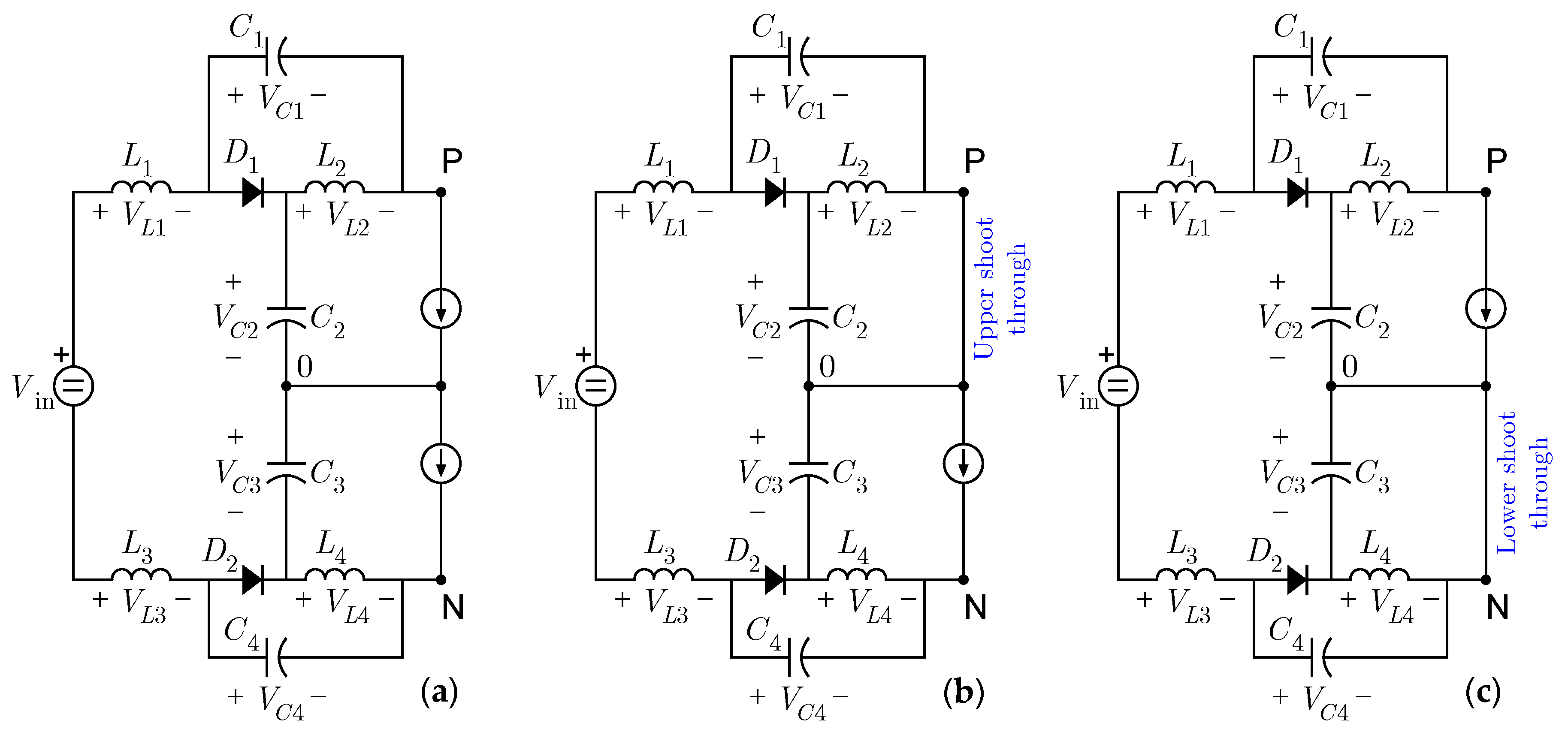
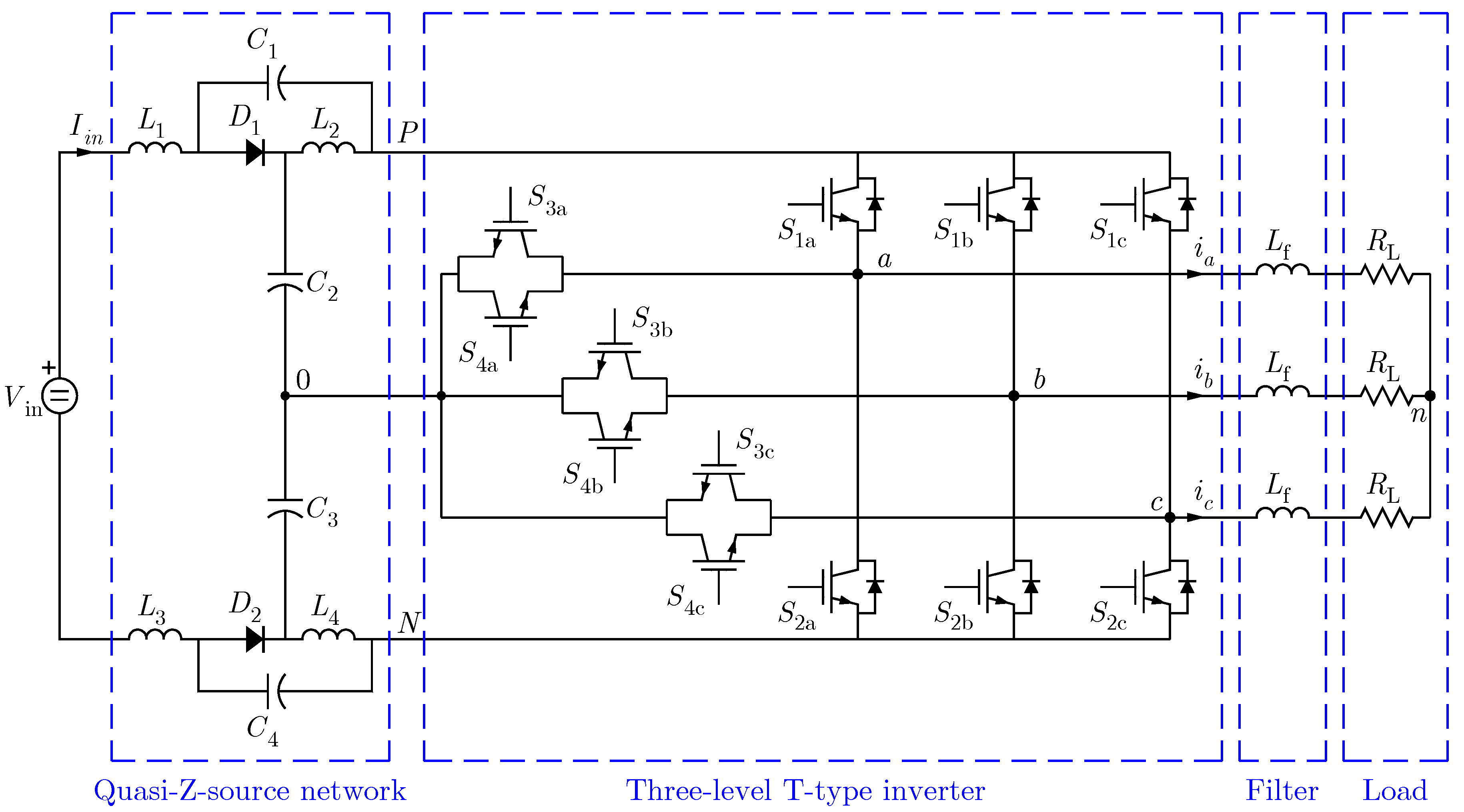
The power circuit is shown in
Figure 1. Two identical quasi-Z-source networks are connected to a common node between capacitors
and
. These networks are linked to a T-type three-level VSI.
2.1. Operation Principle with Upper and Lower Shoot-Through States
By means of diverse switching combinations, a voltage waveform with three possible voltage levels,
, 0, and
, was obtained at each converter leg. In the switching scheme used in a traditional three-level VSI, the output of each phase (
a,
b,
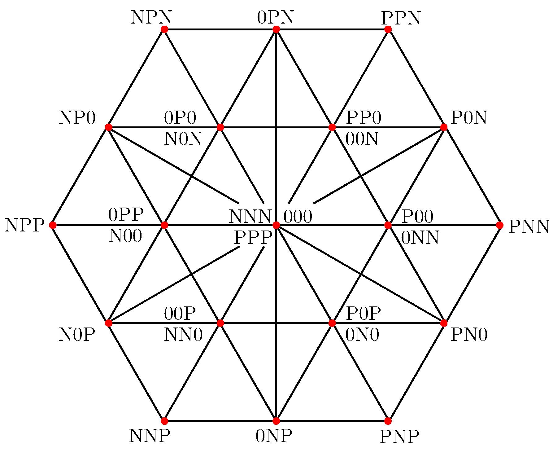
c) can be in either P-, 0-, or N-state (i.e., connected to the positive (P), the neutral (0), or the negative (N) terminal, respectively). Three phases and three states were combined to form 27 valid switching states, depicted in
Figure 2, in the well-known space vector representation for a three-level converter.
There was one extra zero state when the load terminals were shorted through the on state of both the upper and lower switches ( and ) of any phase leg, combinations of any two phase legs, or all three phase legs. This ST zero state was not allowed in the traditional VSI because it caused a short circuit of the capacitors on the DC side. However, thanks to the quasi-Z-source network, ST states were allowed. Energy was stored in the inductors during ST states. Then, during the non-shoot-through (NST) states (comprising the 27 states of the conventional three-level VSI inverter), it was transferred to the capacitors and the load. By means of adjusting the ST duty cycle, the peak DC-link voltage was controlled, and, therefore, the inverter was provided with the desired buck-boost feature.
The ST state described was the so-called full shoot-through (FST) mode, in which short-circuits in the full DC-link, connecting terminals P with N, were produced. Besides the FST state used in the majority of the previous works, two new switching states named UST and LST states emerged in [
29]. The UST state corresponds to the simultaneous activation of switches
and
in a phase leg. It produces a short circuit in the upper half DC-link, connecting terminals P and 0. On the other hand, the LST state takes place when switches
and
in a phase branch are simultaneously turned on. This produces a short circuit in the lower half DC-link, connecting the terminals 0 and N. Application of these new states reduces the harmonic distortion of the output line-to-line voltage compared to the FST.
Table 1 describes the mentioned states for the phase-
a case.
Figure 3 includes the three equivalent circuits in NST, UST, and LST states, respectively.
,
, and
define NST, UST, and LST state durations, respectively. The corresponding duty ratios are
,
, and
, where
T is the switching period
. With the aim of ensuring symmetric operation,
and
are set to be equal
. If the quasi-Z-source network is assumed to be symmetric (i.e.,
,
,
, and
), the voltages across the inductors and capacitors are
,
,
, and
. Continuous conduction mode was assumed for the converter operation as well. Then, as the average voltage across inductors during one switching period should be zero in steady state, the boost factor (defined as
, where
is the peak DC-link voltage, present during NST states) can be calculated by the following Equation, [
30]:
Therefore, the amplitude of the fundamental output phase-to-neutral voltage is given by
where
m is the modulation index.
2.2. New Carrier-Based Modulation Method
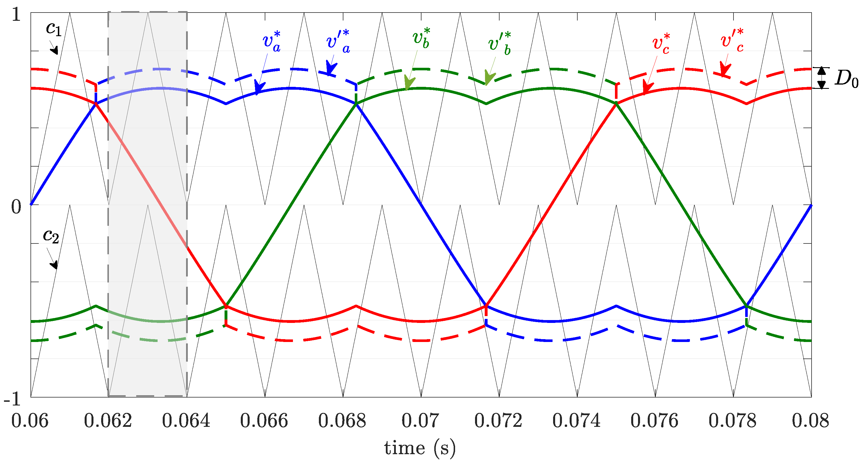
A carrier-based level-shifted PWM (LS-PWM) with a modified constant boost control (MCBC) was proposed. Details of this novel modulation technique application are discussed below.
The reference and carrier signals are displayed in
Figure 4 for the case of
m = 0.7 and
. A switching frequency value of 500 Hz (i.e., a frequency modulation index
) was used for better visualization. Three modulating signals
,
, and
were used as in the traditional PWM scheme. These signals were obtained by using the well-known technique based on the addition of a common offset voltage,
Voff, to the three phase references [
17,
31]:
This approach permitted the modulation index
m to be increased, avoiding the problems associated with overmodulation. In addition, it improved the waveform quality and reduced the switching losses significantly [
32].
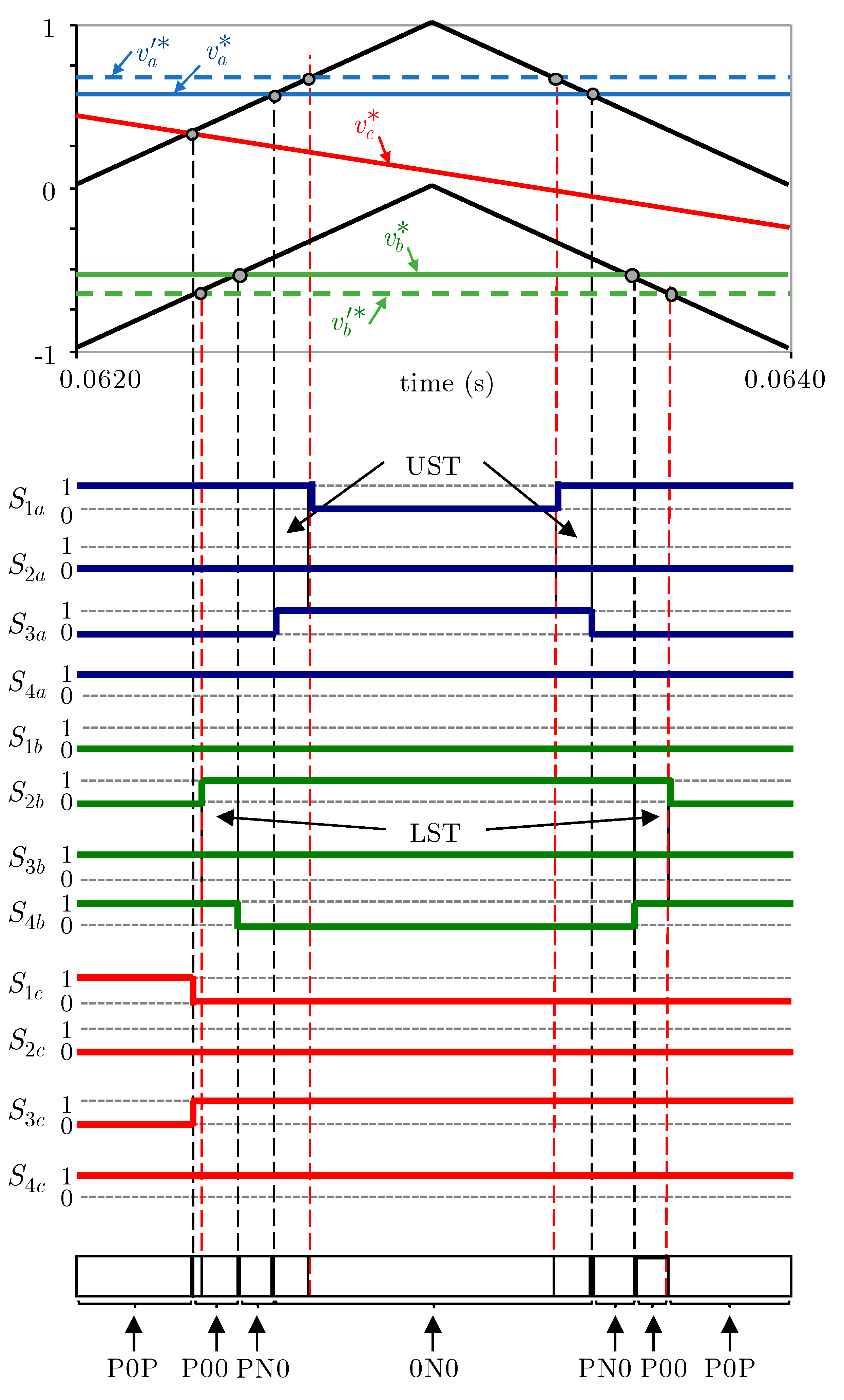
Another three modulating signals, , , and , were generated by shifting up and down the envelope of , , and by the ST duty cycle (). Then, the switching signals (including the ST states) were obtained by comparing the two sets of modulation signals with the two vertically disposed in-phase carrier signals, and , generating the upper and lower ST states (just one phase-leg; a, b, or c was shot-through).
Gate signal generation for switches
to
(
x =
a,
b, and
c) is demonstrated in
Figure 5 for the switching cycle highlighted in
Figure 4 (0.0620 s to 0.0621 s).
and
would have complementary states to
and
, respectively, if there were no ST states. The existence of those states (UST and LST) can be observed on the overlapping of the corresponding on-states, pointed out in
Figure 5.
By using these six reference signals, the converter was modulated as follows: for a phase-leg x, was turned on when was greater than , and was turned on when was smaller than . On the other hand, was turned on when was smaller than , and was turned on when was greater than .
It is interesting to note that to maintain the volt-second average per switching cycle, UST states should be added into the inverter states with the P terminal unconnected. These states are called N-type small vectors in [
20], and they are the states P00, PP0, 0P0, 0PP, 00P, and P0P in
Figure 2. Similarly, LST states should be added into the inverter states with the N terminal unconnected (i.e., into the so-called P-type small vectors: 0NN, 00N, N0N, N00, NN0, 0N0). One can notice that when the N- and P-type small vectors contain two 0-states, UST and LST states can be achieved in two different ways, depending on the leg used to implement the ST condition. All the UST and LST states are collected in
Table 2, where the letters L and U have been introduced in order to distinguish the NST states, and they must be interpreted as the connection of the corresponding phase-leg to the N or P terminal, respectively. This can be verified in
Figure 5, where the states are P0P, P00, PN0, 0N0, PN0, P00, and P0P. UST insertion was performed in the state 0N0, while LST insertion was carried out in states P0P and P00.
3. Simulation Results
The proposed approach was tested through a simulation study using the PSCAD (version X4 (4.5), Manitoba HVDC Research Centre, Winnipeg, Canada, 2014) simulation tool. The parameters of the chosen quasi-Z-source network (
Figure 1) were
and
, and the switching frequency was set at 10 kHz. A DC power supply of 500–800 V was used as inverter input, emulating the operation of a PV array. The converter supplied a balanced, three-phase, wye-connected resistive load,
, at 230/400 V and 50 Hz. A simple inductive filter was used with inductance
.
Simulation results of input voltage and current (
,
), DC-link voltage (
), line-to-line voltages before filtering (
,
, and
), and output currents (
,
, and
) are shown in
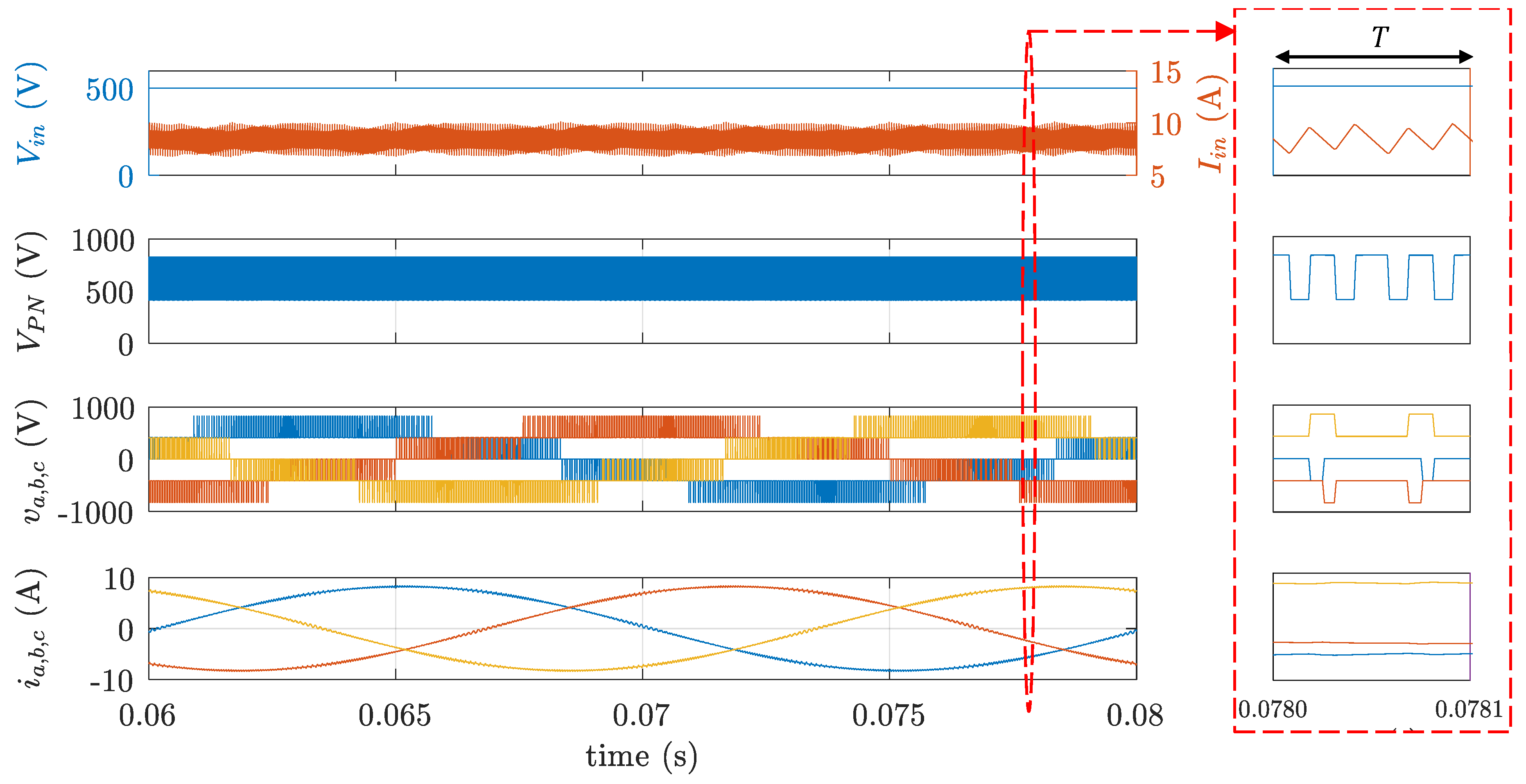
Figure 6 for the nonboosting case and in
Figure 7 using the novel application of UST/LST pulse with modulation approach. In order to show the improvements achieved, the traditional FST strategy was tested by simulation, and the main waveforms were shown in
Figure 8. These cases are discussed in the following paragraphs.
First, it was assumed that the output voltage of the PV array was at its maximum value of 800 V. In this case, to synthesize the required output grid voltage (in the range 380–420 V line-to-line RMS), the modulation index and UST/LST duty cycle were fixed to
m = 0.8 and
. Boost operation was not needed, so the inverter operated in the VSI mode.
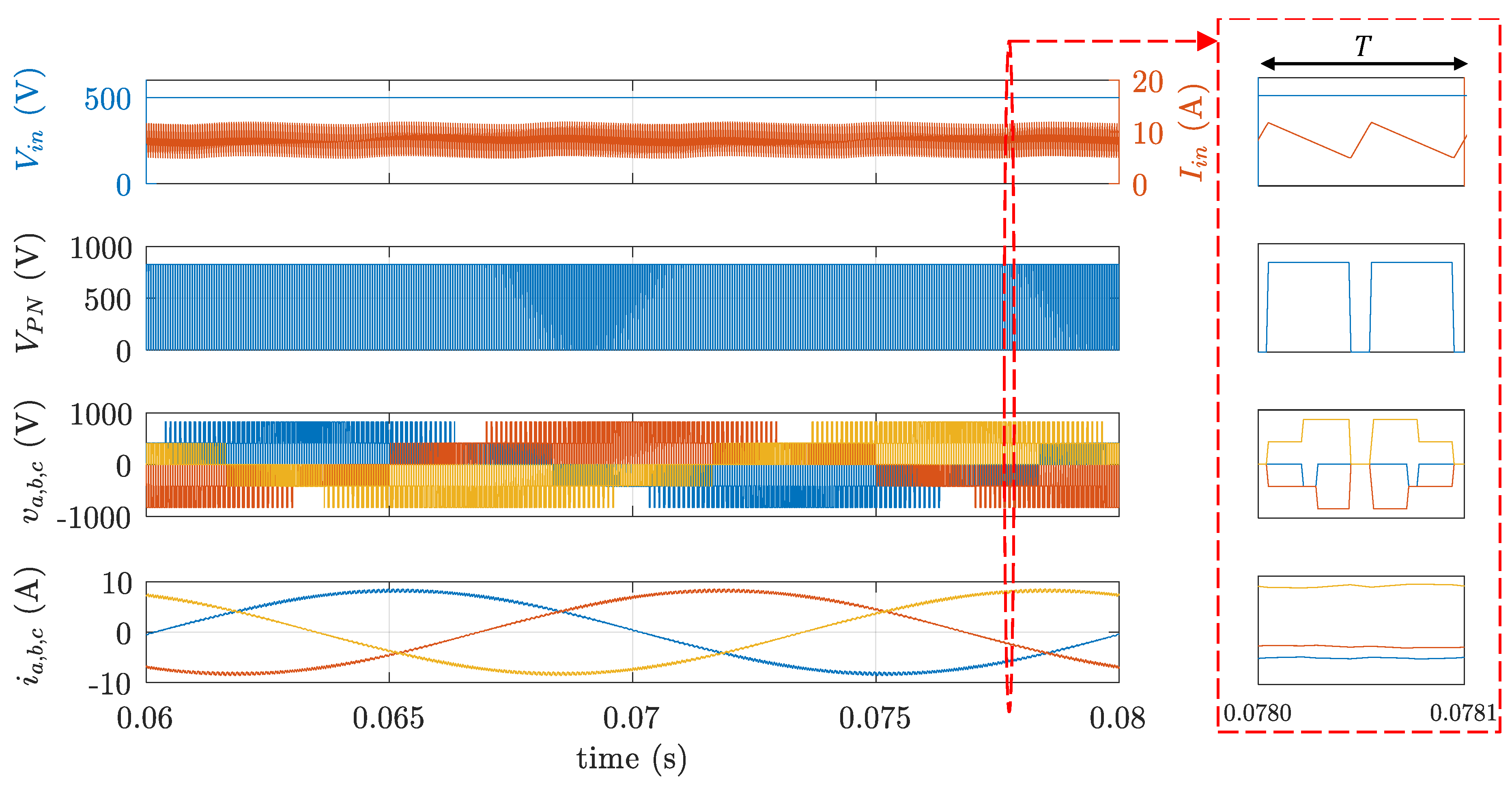
Figure 6 shows the simulated waveform for this case. The current drawn from the PV array (
) was almost ripple-free since no shoot-through states were activated. The DC-link voltage (
) was not boosted (
B = 1), and it was maintained at almost 800 V. The output line-to-line voltages (
) were composed of the levels 0, ±800/2 V, and ±800 V. The RMS value of the fundamental component was 390.9 V, which was within the desired range. The corresponding phase-to-neutral peak voltage of 319.16 V matched the expected value, according to Equation (2).
Next, to illustrate the boost performance operation, the PV panels output was at its minimum value of 500 V (due to bad weather, for example). Now, to synthesize the required output voltage to the grid, a boost operation was needed. This was achieved by maintaining the modulation index at 0.8 and changing the ratio
to 0.2. The results are shown in
Figure 7. Now, the current from the PV array was in continuous conduction mode, with ripples resulting from the shoot-through states. The DC-link voltage was boosted, assuming two levels:
and
, where
was the boost factor (i.e., almost 827 V and 827/2 V). This was a unique feature of the UST/LST strategy, while for the FST strategy the levels were
and 0. The output line-to-line voltages were composed of the levels 0,
, and
(i.e., 0, ±827/2, and ±827 V). The RMS value of the fundamental component was in this case 404.9 V, which was within the desired range. According to Equation (2), the corresponding phase-to-neutral peak voltage of 330.6 V was in good agreement with the expected value. In both cases, high-quality sinusoidal line currents were also obtained.
It is interesting to note that there were slight errors between the expected and simulated values, since the voltage dropped across the diodes and the inductors and were not considered when deriving the equations.
To show the waveform differences and the improved harmonic performance of the proposed UST/LST strategy, compared to the FST strategy, a simulation test using the FST strategy was also carried out. In this case, an FST duty cycle
was applied. The results are shown in
Figure 8.
Observing
Figure 7 and
Figure 8, some of the advantages obtained by using the new UST/LST strategy compared to the conventional FST strategy were directly proven. Switches
and
(see
Figure 1) had to block
. Thus, semiconductors with less blocking voltage capability were required, reducing the cost and the size of the power converter. For the same reason, less EMI can be expected. Hence, the complexity of the control and measurement systems was reduced substantially.
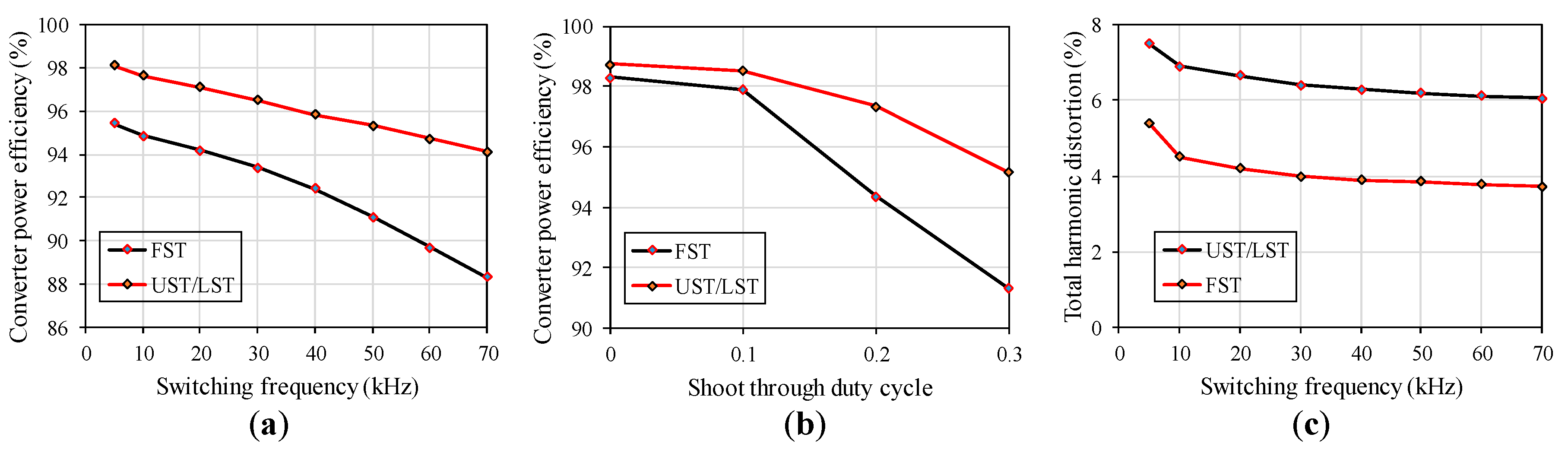
At the same time, switching losses were determined as the energy that a semiconductor needed to switch on and switch off. The lower the blocking voltage, the fewer the switching losses were expected. To illustrate switching loss improvement, simulation tests were conducted applying the two strategies for several values of ST duty cycle,
for UST/LST and
for FST, where the modulation index was set at
or
, respectively. The influence of the switching frequency with constant
in the converter efficiency for UST and UST/LST was also studied. The load was the same as before (40 Ω in the wye connection), and the input voltage was adjusted according to
or
to obtain the same output phase-to-neutral voltage (230 V) in all cases. The results, displayed in
Figure 9, showed that the efficiency decreased with increasing ST duty cycle and with increasing switching frequency. However, the reduction was substantially lower for the proposed strategy. In other words, the new strategy exhibited lower global losses (conduction and switching). It is interesting to point out that this reduction mainly was due to switching loss decreases because the proposed strategy implied half the value of the semiconductor blocking voltage in the traditional strategy. Furthermore, for the same reason, semiconductor device stress was also reduced.
Voltage total harmonic distortion (THD), as a function of the
or
, was measured. The quality of the output voltage was higher with the new UST/LST for any value of the shoot-through duty cycle. This fact was predicted by comparing the magnitudes of line-to-line voltages before filtering (
,
, and
) from
Figure 7 and
Figure 8.
Table 3 sums up performance comparisons of UST/LST and FST strategies in terms of voltage THD (calculated up to 500 harmonics) before filtering, power efficiency, semiconductor stress, and the complexity of implementation, and it points out the advantages of the proposed strategy. In addition, the fact that this strategy was a carrier-based type also implied advantages in its practical implementation; therefore, it is a competitive alternative for quasi-Z-source T-type inverter modulation.

 ,
, 


