Design of a 41.14–48.11 GHz Triple Frequency Based VCO


Abstract
:1. Introduction
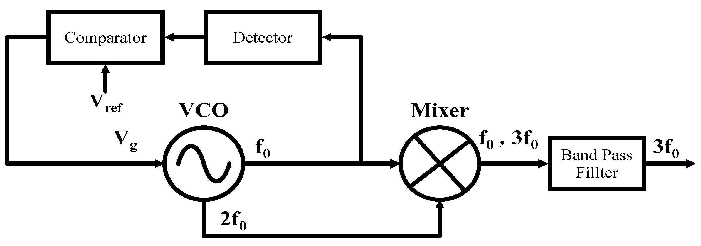
2. Circuit Design
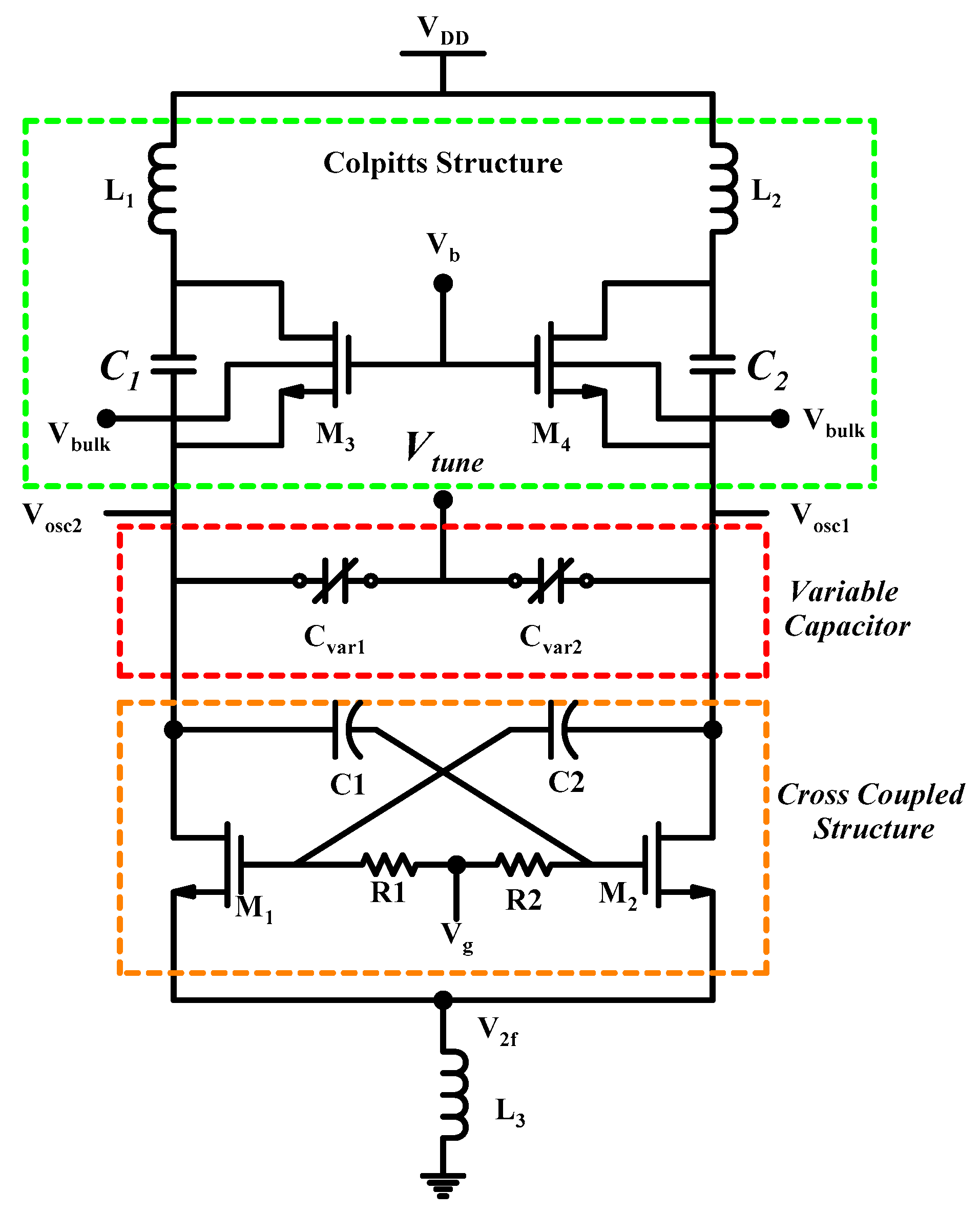
2.1. Voltage Controlled Oscillator
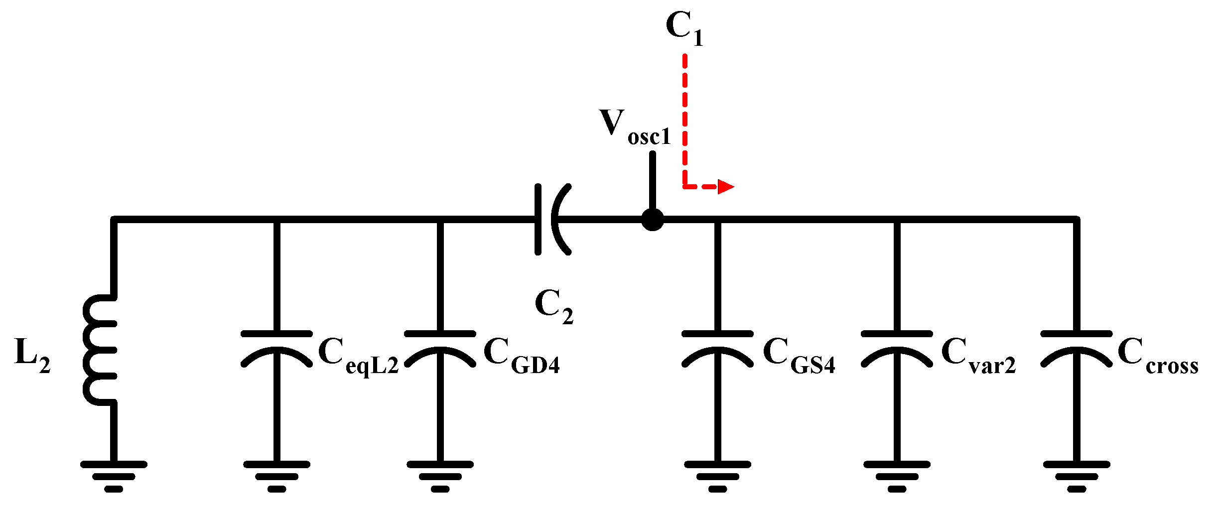
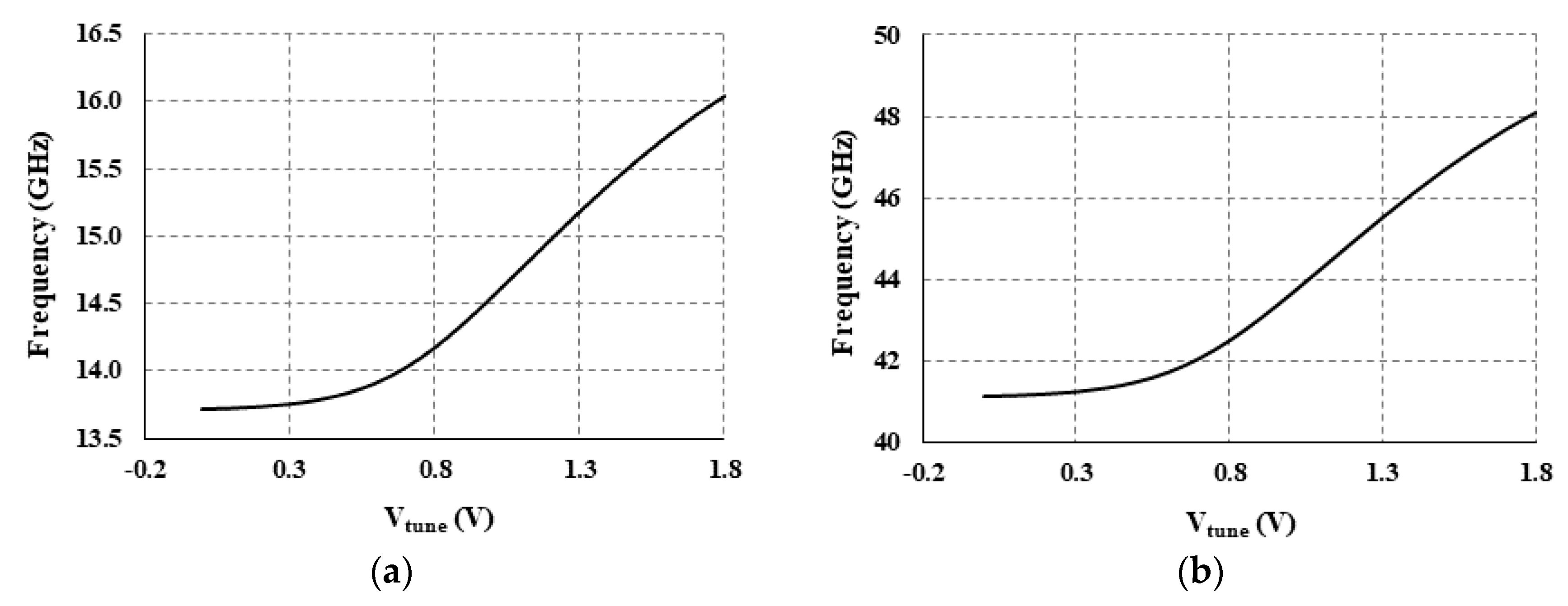
2.1.1. Oscillation Frequency
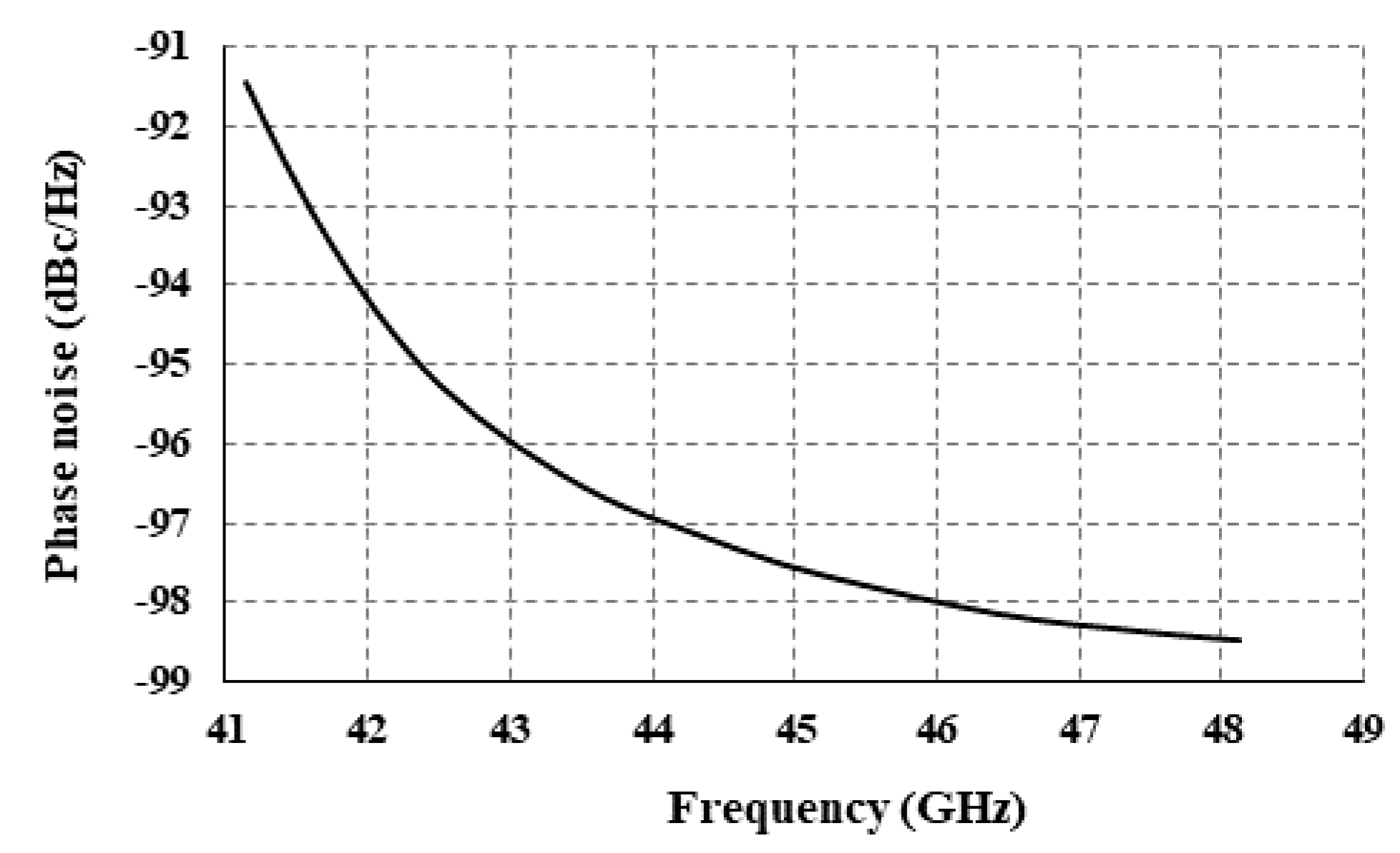
2.1.2. Phase Noise
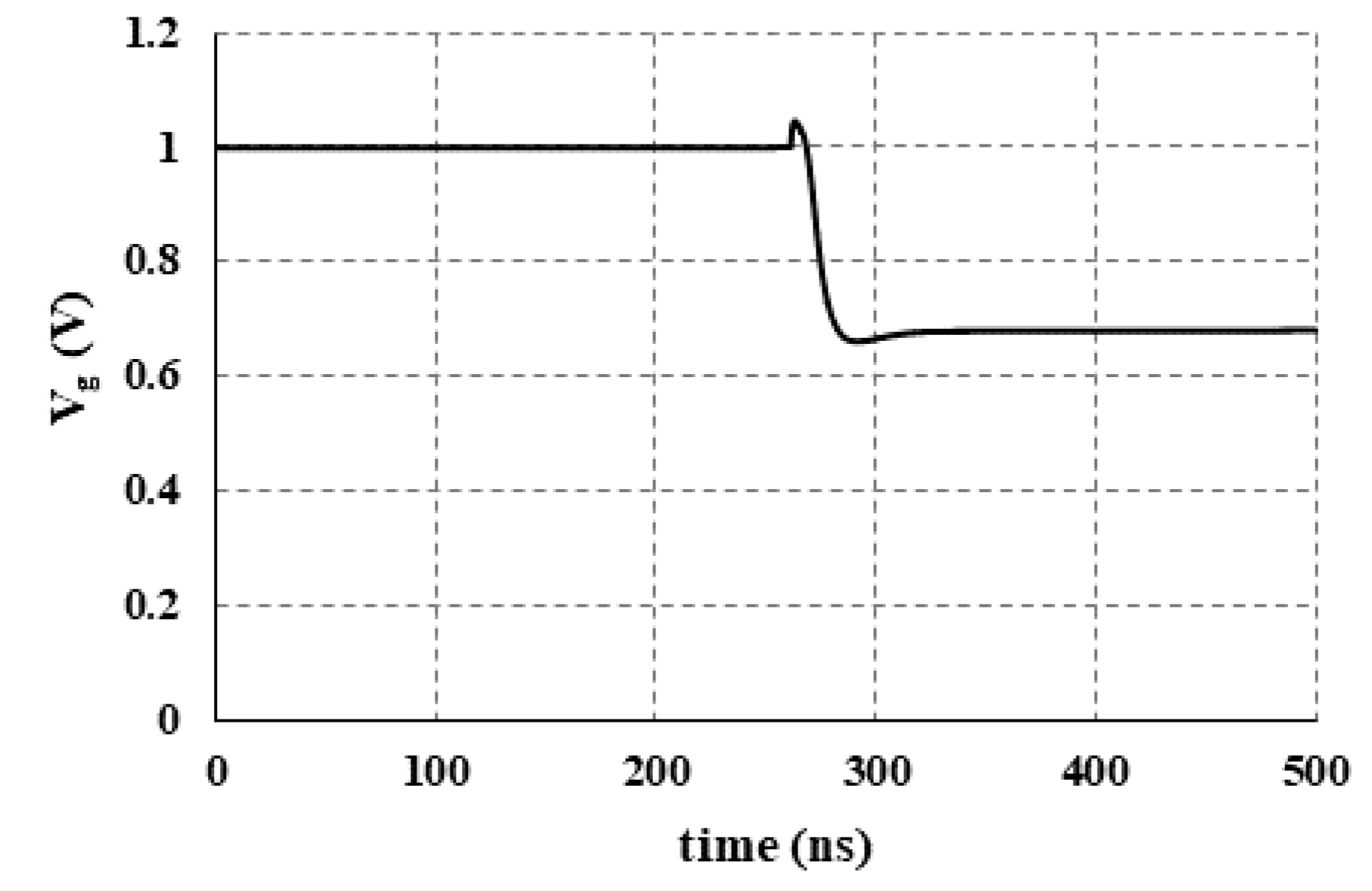
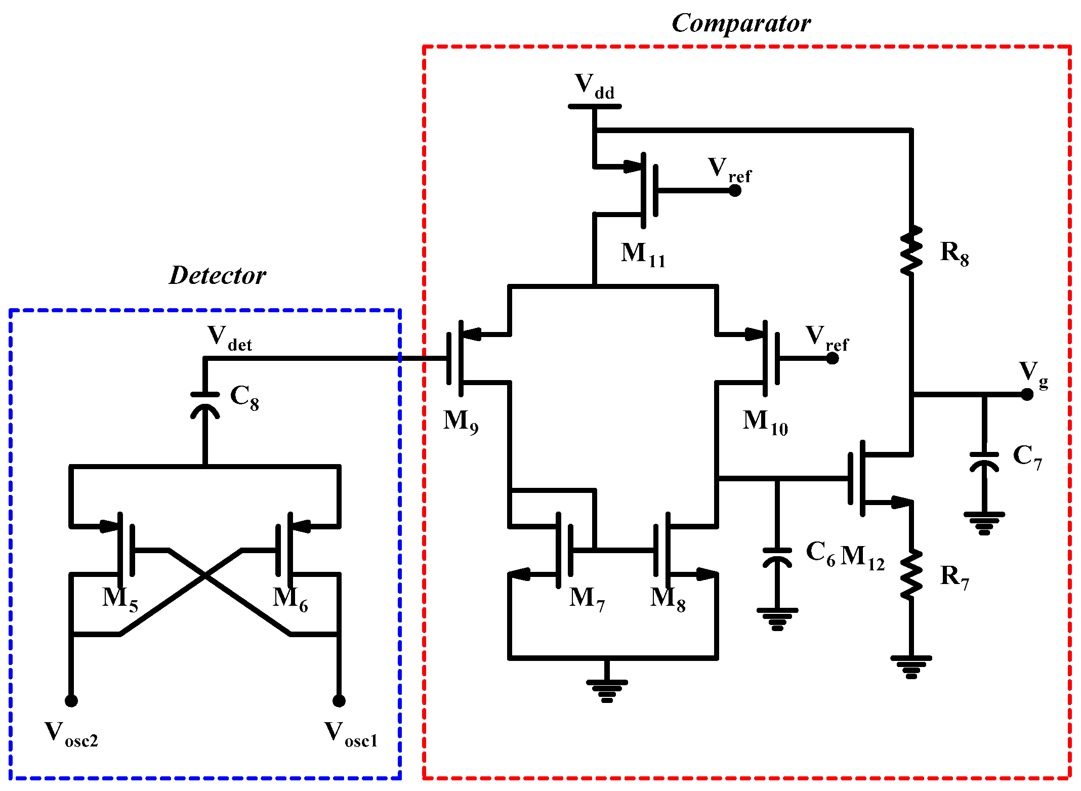
2.2. Amplitude Detector and Comparator
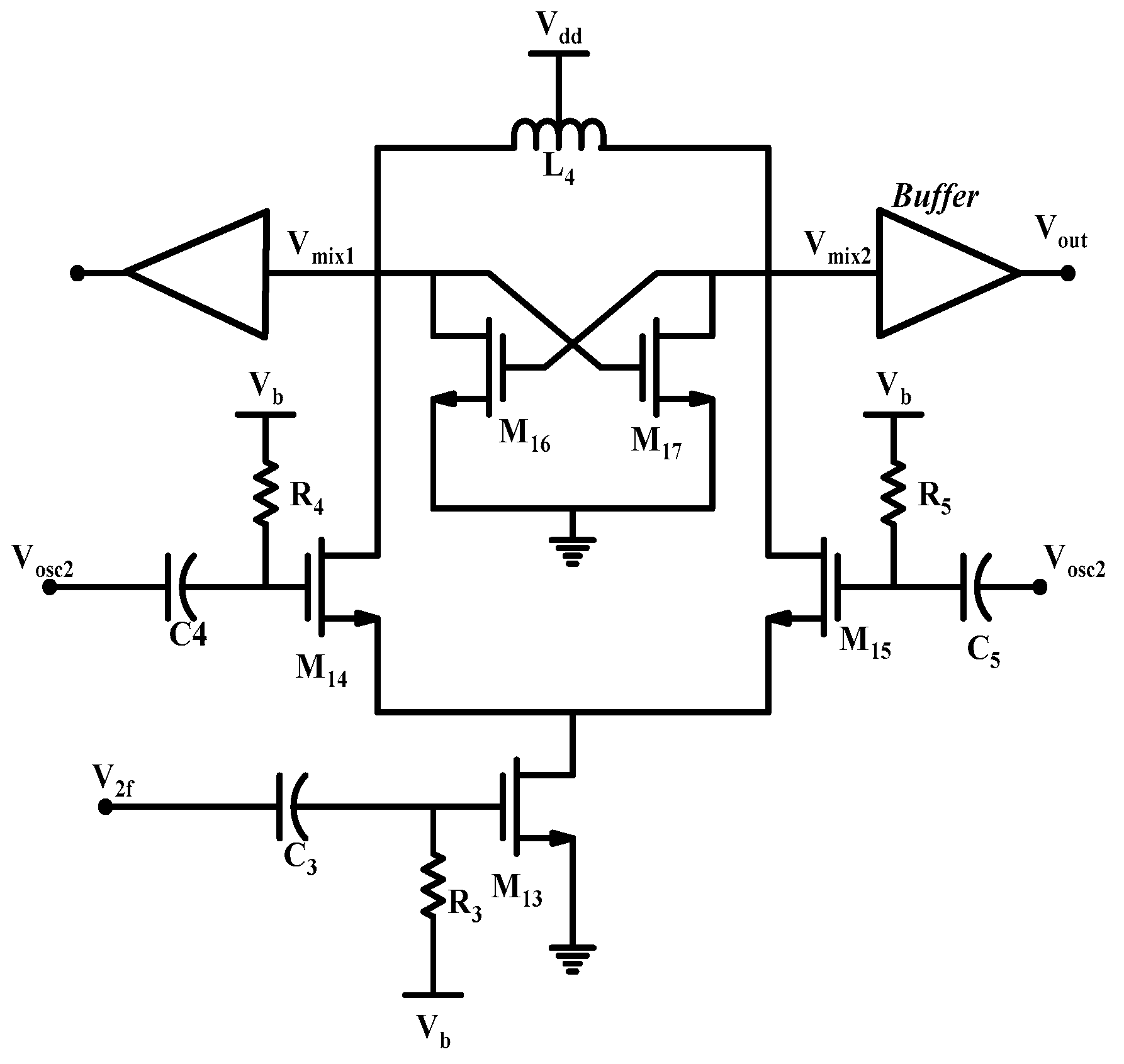
2.3. Designing Mixer
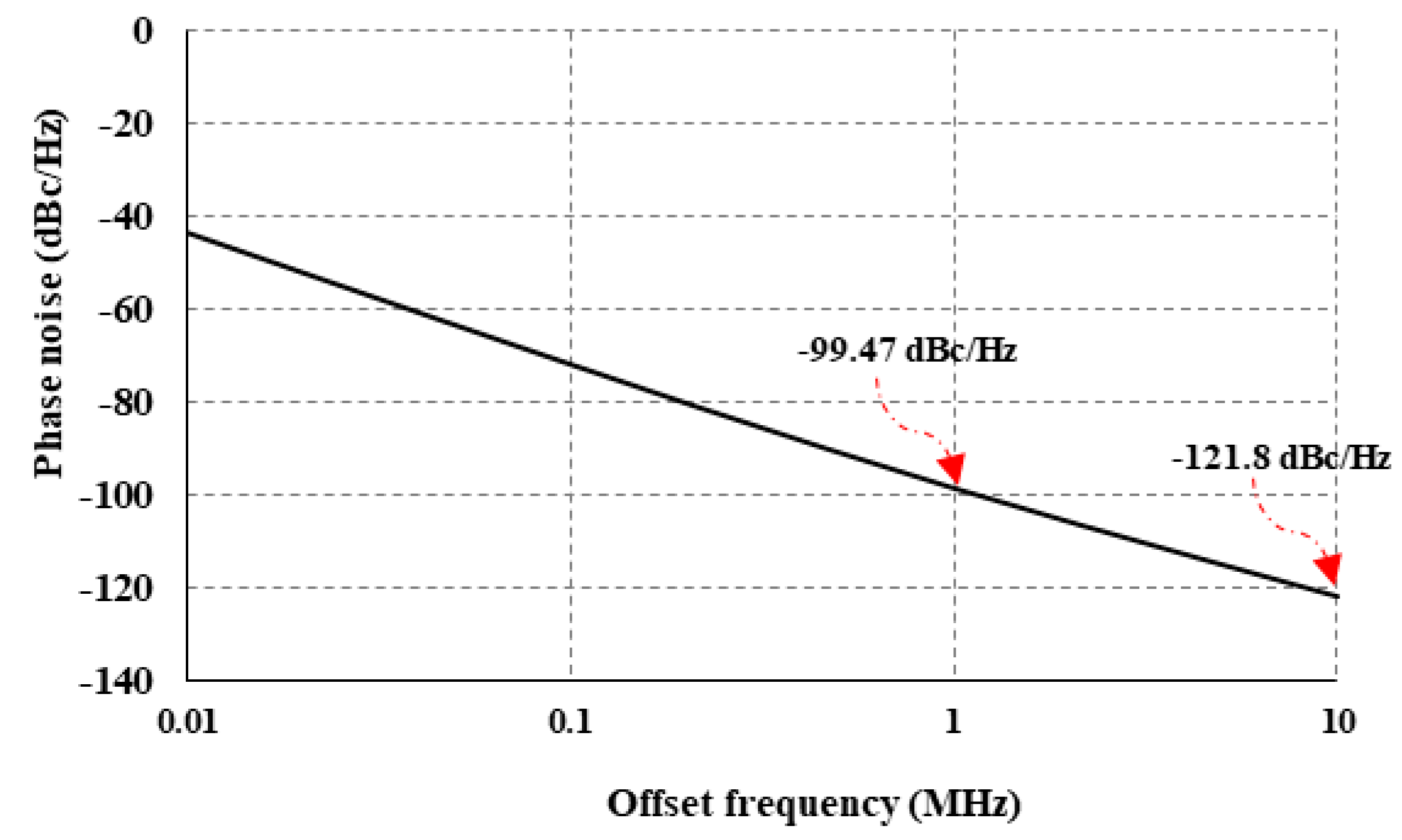
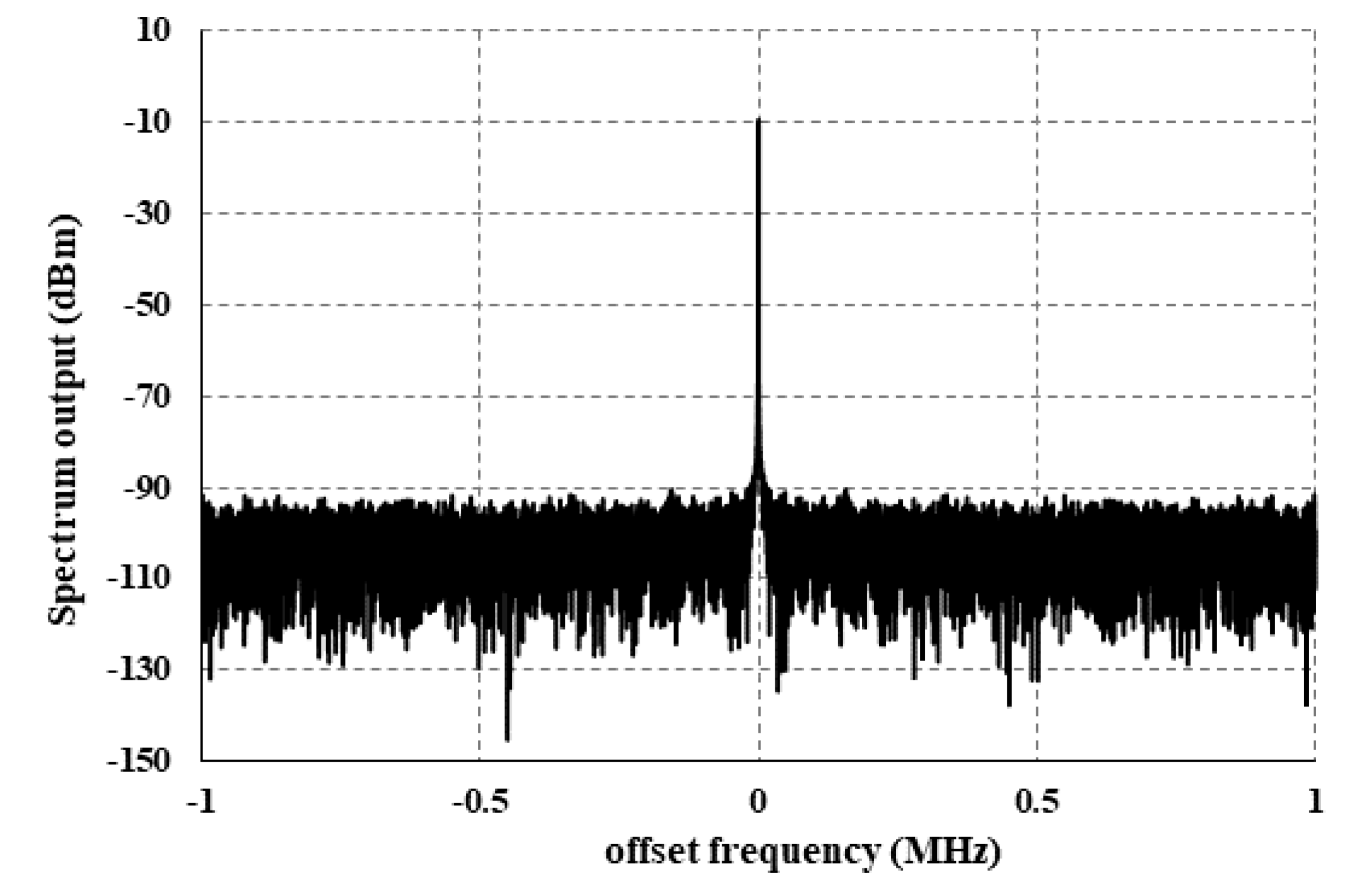
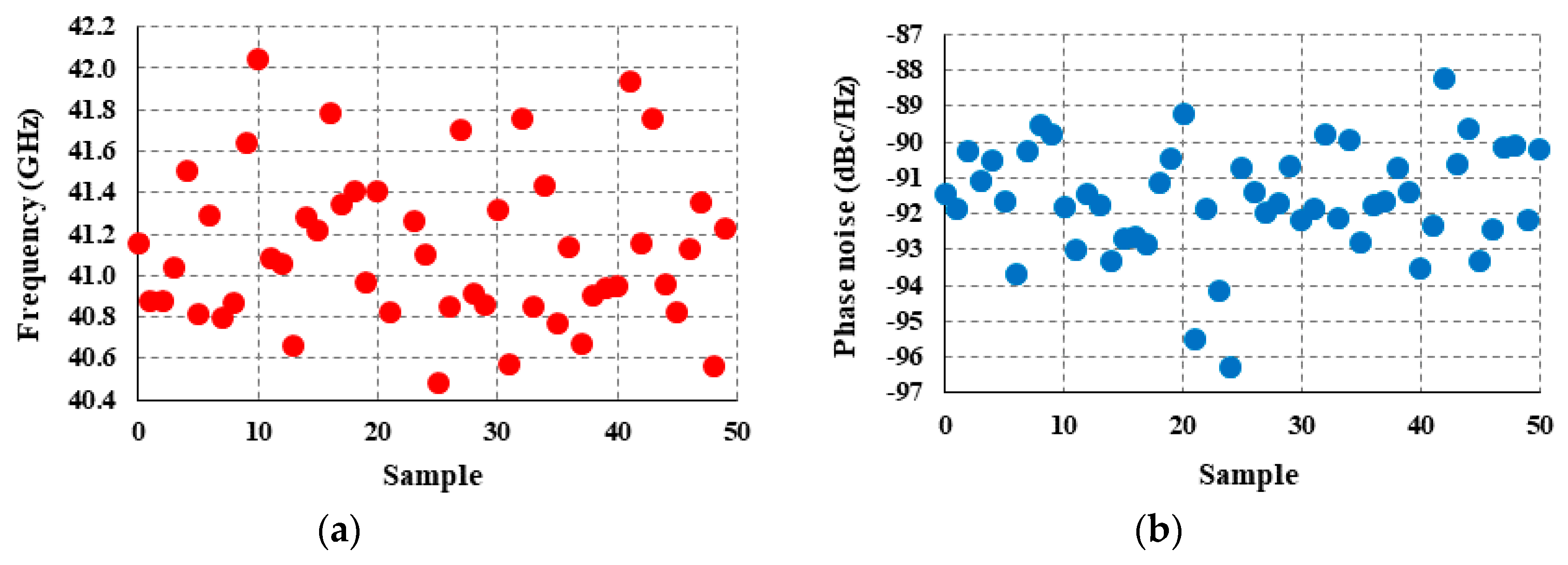
3. Results
4. Conclusions
Author Contributions
Funding
Conflicts of Interest
References
- Estebsari, M.; Gholami, M.; Ghahramanpour, M.J. A Wide Range Delay Locked Loop for Low Power and Low Jitter Applications. Int. J. Circuit Theory Appl. 2018, 46, 401–414. [Google Scholar] [CrossRef]
- Estebsari, M.; Gholami, M.; Ghahramanpour, M.J. A Novel Charge Pump with Low Current for Low-Power Delay-Locked Loops. Circuits Syst. Signal Process. 2017, 36, 3514–3526. [Google Scholar] [CrossRef]
- Xu, X.; Chen, C.; Sugiura, T.; Yoshimasu, T. 18-GHz Band Low-Power LC VCO IC Using LC Bias Circuit in 56-nm SOI CMOS. In Proceedings of the IEEE Asia Pacific Microwave Conference (APMC), Kuala Lumpar, Malaysia, 13–16 November 2017; pp. 938–941. [Google Scholar]
- Shirazi, A.H.M.; Nikpaik, A.; Molavi, R.; Lightbody, S.; Djahanshahi, H.; Taghivand, M.; Mirabbasi, S.; Shekhar, S. On the Design of mm-Wave Self-Mixing-VCO Architecture for High Tuning-Range and Low Phase Noise. IEEE J. Solid-State Circuits 2016, 51, 1210–1222. [Google Scholar] [CrossRef]
- Sotner, R.; Jerabek, J.; Langhammer, L.; Dvorak, J. Design and Analysis of CCII-Based Oscillator with Amplitude Stabilization Employing Optocouplers for Linear Voltage Control of the Output Frequency. Electronics 2018, 7, 157. [Google Scholar] [CrossRef]
- Yargholi, M.; Nasri, A. A Low Phase Noise LC VCO for 6GHz. International Conference on Data Mining. In Proceedings of the Electronics and Information Technology, Pattaya, Thailand, 10–11 August 2015; pp. 10–11. [Google Scholar]
- Jain, S.; Jang, S.L.; Tchamov, N.T. Tuned LC-Resonator Dual-Band VCO. IEEE Microw. Wirel. Compon. Lett. 2016, 26, 204–206. [Google Scholar] [CrossRef]
- Li, B.; Wu, Y.; Yu, C.; Liu, Y. Independently Tunable Concurrent Dual-Band VCO Using Square Open-Loop Resonator. IEEE Access 2018, 6, 12634–12641. [Google Scholar] [CrossRef]
- Ullah, F.; Liu, Y.; Li, Z.; Wang, X.; Sarfraz, M.M.; Zhang, A. A Bandwidth-Enhanced Differential LC-Voltage Controlled Oscillator (LC-VCO) and Superharmonic Coupled Quadrature VCO for K-Band Applications. Electronics 2018, 7, 127. [Google Scholar] [CrossRef]
- Ali, I.; Aftab, M.A.; Hussain, S.M.S. Performance Comparison of IEC 61850-90-5 and IEEE C37.118.2 Based Wide Area PMU Communication Networks. J. Mod. Power Syst. Clean Energy 2016, 4, 487–495. [Google Scholar] [CrossRef]
- Guo, H.; Chen, Y.; Mak, P.; Martins, R.P. A 0.083-mm2 25.2-to-29.5 GHz Multi-LC-Tank Class-F234 VCO with a 189.6-dBc/Hz FOM. IEEE Solid-State Circuits Lett. 2018, 1, 86–89. [Google Scholar] [CrossRef]
- Kim, B.I. Direct Comparison between Phase Locked Oscillator and Direct Resonance Oscillator in the Noncontact Atomic Force Microscopy under Ultrahigh Vacuum. Rev. Sci. Instrum. 2004, 75, 5035–5037. [Google Scholar] [CrossRef]
- Hsieh, M.; Sobelman, G.E. Comparison of LC and Ring VCOs for PLLs in a 90 nm Digital CMOS Process. In Proceedings of the International SOC Design Conference, Busan, Korea, 19–22 October 2006; pp. 19–22. [Google Scholar]
- Kashani, M.H.; Tarkeshdouz, A.; Molavi, R.; Afshari, E.; Mirabbasi, S. A Wide-Tuning-Range Low-Phase-Noise mm-Wave CMOS VCO with Switchable Transformer-Based Tank. IEEE J. Solid-State Circuits Lett. 2018, 1, 82–85. [Google Scholar] [CrossRef]
- Katebi, M.; Nasri, A.; Toofan, S. Low-Power VCO for K-band Applications. In Proceedings of the Iranian Conference on International Electrical Engineering (ICEE), Mashhad, Iran, 8–11 May 2018; pp. 144–149. [Google Scholar]
- Xi, T.; Guo, Sh.; Gui, P.; Huang, D.; Fan, Y.; Morgan, M. Low-Phase-Noise 54-GHz Transformer-Coupled Quadrature VCO and 76-/90-GHz VCOs in 65-nm CMOS. IEEE Trans. Microw. Theory Tech. 2016, 64, 2091–2103. [Google Scholar] [CrossRef]
- Jovanovic, G.; Stojcev, M.; Stamenkovic, Z. A CMOS Voltage Controlled Ring Oscillator with Improved Frequency Stability. Sci. Publ. State Univ. NoviPazar 2010, 2, 1–9. [Google Scholar]
- Jalalifar, M.; Byun, G.S. Design of Ku-Band Transformer-Based Cross-Coupled Complementary LC-VCO. Electron. Lett. 2015, 51, 832–834. [Google Scholar] [CrossRef]
- Katebi, M.; Nasri, A.; Toofan, S. A Wide Tuning Range and Low Phase Noise VCO Using New Capacitor Bank Structure. Majlesi J. Electr. Eng. 2018, 12, 95–103. [Google Scholar]
- Aparicio, R.; Hajimiri, A. A Noise-Shifting Colpitts Differential VCO. IEEE J. Solid-State Circuits 2002, 37, 1728–1736. [Google Scholar] [CrossRef]
- Wang, T.P. A CMOS Colpitts VCO Using Negative-Conductance Boosted Technology. IEEE Trans. Circuits Syst. I 2011, 58, 2623–2635. [Google Scholar] [CrossRef]
- Zou, Q.; Ma, K.; Yeo, K.S. A Low Phase Noise and Wide Tuning Range Millimeter-Wave VCO Using Switchable Couple d VCO-Core. IEEE Trans. Circuits Syst.-I 2015, 62, 554–563. [Google Scholar] [CrossRef]
- Sun, J.; Boon, C.C.; Zhu, X.; Yi, X.; Devrishi, K.; Meng, F. A Low-Power Low-Phase-Noise VCO with Self-Adjusted Active Resistor. IEEE Microw. Wirel. Compon. Lett. 2016, 26, 201–203. [Google Scholar] [CrossRef]
- Jang, S.L.; Jain, S. Dual C- and S-Band CMOS VCO Using the Shunt Varactor Switch. IEEE Trans. Very Large Scale Integr. (VLSI) Syst. 2015, 23, 1808–1813. [Google Scholar] [CrossRef]
- Zong, Z.; Babaie, M. A 60 GHz Frequency Generator Based on a 20 GHz Oscillator and an Implicit Multiplier. IEEE J. Solid-State Circuits 2016, 51, 1261–1273. [Google Scholar] [CrossRef]
- NiuI, X.; Li, L.; Wang, D. A 50GHz VCO in 65nm LP CMOS for mm-Wave Applications. In Proceedings of the IEEE International Conference on Solid-State and Integrated Circuit Technology (ICSICT), Hangzhou, China, 25–28 October 2016; pp. 149–151. [Google Scholar]
- Allen, P.E.; Douglas, R.H. CMOS Analog Circuit Design; Oxford University Press: Oxford, UK, 1987. [Google Scholar]
- Paydavosi, N.; Morshed, T.H.; Lu, D.D.; Yang, W.; Dunga, M.V.; Xi, X.J.; He, J.; Liu, W.; Cao, M.; Jin, X.; et al. BSIM4v4. 8.0 MOSFET Model-User’s Manual; University of California: Berkeley, CA, USA, 2013. [Google Scholar]
- Razavi, B.; Goodwin, B.; Fuller, J. RF Microelectronics, 2nd edition; Prentice Hall: Upper Saddle River, NJ, USA, 2011. [Google Scholar]
- Lu, L.; Tang, Z.; Andreani, P.; Mazzanti, A.; Hajimiri, A. Comments on “Comments on “A General Theory of Phase Noise in Electrical Oscillators. IEEE J. Solid-State Circuits 2008, 43, 2170. [Google Scholar] [CrossRef]


| Corners | Phase Noise (1 MHz) | Phase Noise (10 MHz) |
|---|---|---|
| Typical-typical (TT) | −99.47 | −121.8 |
| Fast-fast (FF) | −94.41 | −119.57 |
| Slow-slow (SS) | −97.49 | −120.61 |
| Ref. | [3] 2 | [9] 1 | [16] 2 | [25] 2 | [26] 2 | This Work 1 | |
|---|---|---|---|---|---|---|---|
| Process | 56 nm SOI 5 | 0.13 µm CMOS | 65 nm CMOS | 40 nm CMOS | 65 nm CMOS | 0.18 µm CMOS | |
| Frequency (GHz) | 18.57 | 25.5 | 54 | 55.45 | 46.8 | 44.62 | |
| Tuning range (%) | 5.38 | 43 | 9.1 | 25.4 | 5.8 | 15.6 | |
| Phase noise at offset frequency (dBc/Hz) | −117.6 | −96 | −95.5 | −100.1 | −100 | −99.47 | |
| at 5 MHz | at 1 MHz | at 1 MHz | at 1 MHz | at 1 MHz | at 1 MHz | ||
| PDC (mW) | 2.56 | 12 | 24 | 22 | 5 | 14 4 | 4.16 3 |
| Figure of merit (FOM) (dBc/Hz) | −185.1 | −173.33 | −179 | −179.8 | −186.415 | −187.95 4 | −193.22 3 |
| Total figure of merit (FOMT) (dBc/Hz) | −190.43 | −186 | −179.8 | −187.9 | −188.5 | −191.81 4 | −197.08 3 |
© 2019 by the authors. Licensee MDPI, Basel, Switzerland. This article is an open access article distributed under the terms and conditions of the Creative Commons Attribution (CC BY) license (http://creativecommons.org/licenses/by/4.0/).
Share and Cite
Nasri, A.; Toofan, S.; Estebsari, M.; Estebsari, A. Design of a 41.14–48.11 GHz Triple Frequency Based VCO. Electronics 2019, 8, 529. https://doi.org/10.3390/electronics8050529
Nasri A, Toofan S, Estebsari M, Estebsari A. Design of a 41.14–48.11 GHz Triple Frequency Based VCO. Electronics. 2019; 8(5):529. https://doi.org/10.3390/electronics8050529
Chicago/Turabian StyleNasri, Abbas, Siroos Toofan, Motahhareh Estebsari, and Abouzar Estebsari. 2019. "Design of a 41.14–48.11 GHz Triple Frequency Based VCO" Electronics 8, no. 5: 529. https://doi.org/10.3390/electronics8050529
APA StyleNasri, A., Toofan, S., Estebsari, M., & Estebsari, A. (2019). Design of a 41.14–48.11 GHz Triple Frequency Based VCO. Electronics, 8(5), 529. https://doi.org/10.3390/electronics8050529