Article

Compact Convolutional Neural Network Accelerator for IoT Endpoint SoC

1
College of Electronic and Information Engineering, Nanjing University of Aeronautics and Astronautics, Nanjing 211106, China
2
Science and Technology on Electronic Information Control Laboratory, Chengdu 610036, China
3
School of Microelectronics, HeFei University of Technology, Hefei 230009, China
*
Author to whom correspondence should be addressed.
Electronics 2019, 8(5), 497; https://doi.org/10.3390/electronics8050497
Submission received: 19 March 2019 / Revised: 27 April 2019 / Accepted: 30 April 2019 / Published: 5 May 2019
(This article belongs to the Special Issue New Applications and Architectures Based on FPGA/SoC)

Abstract

:
As a classical artificial intelligence algorithm, the convolutional neural network (CNN) algorithm plays an important role in image recognition and classification and is gradually being applied in the Internet of Things (IoT) system. A compact CNN accelerator for the IoT endpoint System-on-Chip (SoC) is proposed in this paper to meet the needs of CNN computations. Based on analysis of the CNN structure, basic functional modules of CNN such as convolution circuit and pooling circuit with a low data bandwidth and a smaller area are designed, and an accelerator is constructed in the form of four acceleration chains. After the acceleration unit design is completed, the Cortex-M3 is used to construct a verification SoC and the designed verification platform is implemented on the FPGA to evaluate the resource consumption and performance analysis of the CNN accelerator. The CNN accelerator achieved a throughput of 6.54 GOPS (giga operations per second) by consuming 4901 LUTs without using any hardware multipliers. The comparison shows that the compact accelerator proposed in this paper makes the CNN computational power of the SoC based on the Cortex-M3 kernel two times higher than the quad-core Cortex-A7 SoC and 67% of the computational power of eight-core Cortex-A53 SoC.

1. Introduction

With the development of Internet of Things (IoT) technology and artificial intelligence (AI) algorithms, AI computing has moved from the cloud down to the edge [1]. Intelligent Internet of Things (AI+IoT, AIoT), which integrates the advantages of AI and IoT technology, has become a research hotspot in the related fields of the Internet of Things [2]. The IoT endpoint System-on-Chip (SoC) refers to a large number of MCUs near the sensors in the IoT system, some typical examples of which are STM32, ESP32 and MSP430. As the information collector and command executor in the IoT system, the node SoC contains a large amount of information that can be utilized by artificial intelligence. IoT developers are seeking to implement AI algorithms such as face recognition and speech recognition on resource-constrained IoT endpoint devices [3]. Based on these application demands, some well-known IoT chip manufacturers around the world also provide some AI libraries and solutions for their IoT chips, such as ESP-WHO of ESPRESSIF and STM32Cube.AI of STMicroelectronics. Nevertheless, optimizing and tailoring algorithms only from the software level to adapt the IoT endpoint SoC with limited computing capability is insufficient. It is of great practical significance to develop a smart IoT endpoint chip that is suitable for AIoT from the hardware level.
Convolutional neural network (CNN) is a kind of neural network which consists of a large number of convolution operations and has a certain depth. Due to its good performance in image recognition, CNN can be widely used in IoT scenarios such as home security and face recognition. At present, the common hardware acceleration of CNN mainly depends on GPU, ASIC or FPGA [4]. Most of the research on this kind of CNN hardware acceleration is oriented to servers or high-performance computing centers and the main focus is to accelerate performance while ignoring resource consumption. As stated in [5,6], most of the network structures in CNN are deployed and implemented by hardware. This design can really achieve high computational acceleration performance but it requires great resources and energy overheads which cannot be applied in resource-constrained IoT node devices. In order to design a CNN acceleration unit suitable for an IoT endpoint system, S. Han proposed an efficient hardware acceleration structure based on the sparsity of the neural network by pruning the network appropriately in Ref [7]. At the same time, although many CNN accelerators have computational efficiencies of hundreds of giga operations per second (GOPS), they mostly rely on a highly specialized network structure [8,9], which makes their flexibility very limited and not suitable for IoT systems with diverse application scenarios. For this reason, in [10] a two-dimensional convolution calculation circuit is added to the processor kernel to complete the CNN acceleration for the IoT system. Despite its advantages in resource usage, flexibility and acceleration performance, it requires chip designers to refactor processor kernels, which is a difficult challenge for many IoT chip companies.
The authors have designed a multi-functional CNN accelerator for IoT SoC in [11] to meet the needs of CNN computing in the IoT scenario. This design reduces resource consumption by expanding and reusing basic module circuits. Based on our previous work, this paper further extends a compact CNN accelerator design for the IoT endpoint SoC, which can further improve the performance while reducing the area of the circuit. By analyzing the data characteristics of the two-dimensional convolution, a compact convolution calculation circuit, accumulator and streaming pooling circuits are designed. A multi-functional CNN acceleration chain is constructed using these modules and the compact accelerator is built based on the acceleration chain and some customized storage module. We designed a verification SoC based on the Cortex-M3 kernel, and we tested and analyzed the accelerator on the FPGA. The results show that in various CNN accelerators, the proposed design has achieved the CNN acceleration capability with a small resource consumption, which can meet the CNN computing requirements of an IoT node SoC with limited resources.
The rest of this paper is organized as follows: Section 2 introduces the design of primary function modules, especially the design of the convolution circuit with a low bandwidth occupied. Section 3 details the structure of the convolution accelerator, focusing on the processing of data bit width and the design of the storage module. Section 4 introduces the verification SoC structure based on Cortex-M3 and details the migration of the Lenet-5 network. Section 5 uses Lenet-5 as a test case to compare the performance of the accelerator with some high-performance processors and evaluate the resource consumption. Section 6 summarizes the conclusions of this work.

2. Function Module Design

At present, some mainstream CNN algorithms are composed of four parts: convolution layer, activation layer, pooling layer and full connection (FC) layer. Most state-of-the-art neural networks contain a large number of convolution layers, such as VGG-16 which contains at least 13 convolution layers and Alexnet which contains five convolution layers, so the acceleration of the convolution operation is the focus of this CNN accelerator. Activation layers and pooling layers are relatively simple in the algorithm, but as they closely follow the convolution layers, the number of layers is quite large, so this also needs to be accelerated by hardware. Although the full connection layer involves the most CNN parameters, its hardware implementation is similar to convolution, which can be understood as a special form of convolution operation. Essentially, in [12] it is also mentioned that the FC layer is not very meaningful in practical applications. Therefore, we focused on the design of the convolution layer.

2.1. Notation

  • K: width of convolution kernels
  • N: width of input feature maps
  • Ln: maximum number of connections between convolution kernels and input feature map
  • psum: the partial sum of convolution
  • Src A: source matrix read-channel
  • Src B: convolution kernel matrix read-channel
  • Src C: accumulative value read-channel
  • Result: calculation results store-channel

2.2. Convolution Unit

In the CNN convolution layer, high-dimensional convolution is calculated by accumulating multiple two-dimensional (2-D) convolutions. The basic expression of the CNN convolution layer can be expressed as Equation (1).
o f m a p [ z ] = k = 1 M i f m a p [ k ] * W [ z ] [ k ]
where ifmap and ofmap represent the input and output feature map, z denotes the output feature map number, W denotes the weight of convolution kernel, k denotes the input feature map number, and ‘*’ denotes the 2-D convolution calculation.
According to [13], 2-D convolution is the most basic and important operation in CNN, and it consumes more than 90% of the total computational time. Thereby, 2-D convolution is always the focus of many CNN accelerators’ optimization. Furthermore, convolution operation contains a large amount of data loading-storage, but in fact, this data has a lot of repetition [14]. 2-D Convolution operations of matrix X with N*N size and convolution kernel W with K*K size can be expressed by Equation (2).
Y ( s , t ) = m = 0 K 1 n = 0 K 1 X ( s m , t n ) × W ( m , n )     0 s N + K 1 ,   0 t N + K 1
According to Equation (2), the total data to be loaded to complete the convolution is K × K × (N – K + 1) × (N – K + 1). However, the actual amount of data needed for convolution is only N × N. If the repeatability of convolution data can be effectively utilized, not only the convolution can be accelerated but also memory access bandwidth can be reduced. In particular, for resource-constrained IoT endpoint SoC, the processor kernel and the CNN accelerator often share the on-chip memory. The reduced bandwidth usage of the CNN accelerator enables the processor kernel to release its computing power and further improve the overall performance of SoC.
In this paper, a 2-D convolution computing unit is designed to decrease the memory bandwidth by utilizing the data repeatability. Its structure is shown in Figure 1.
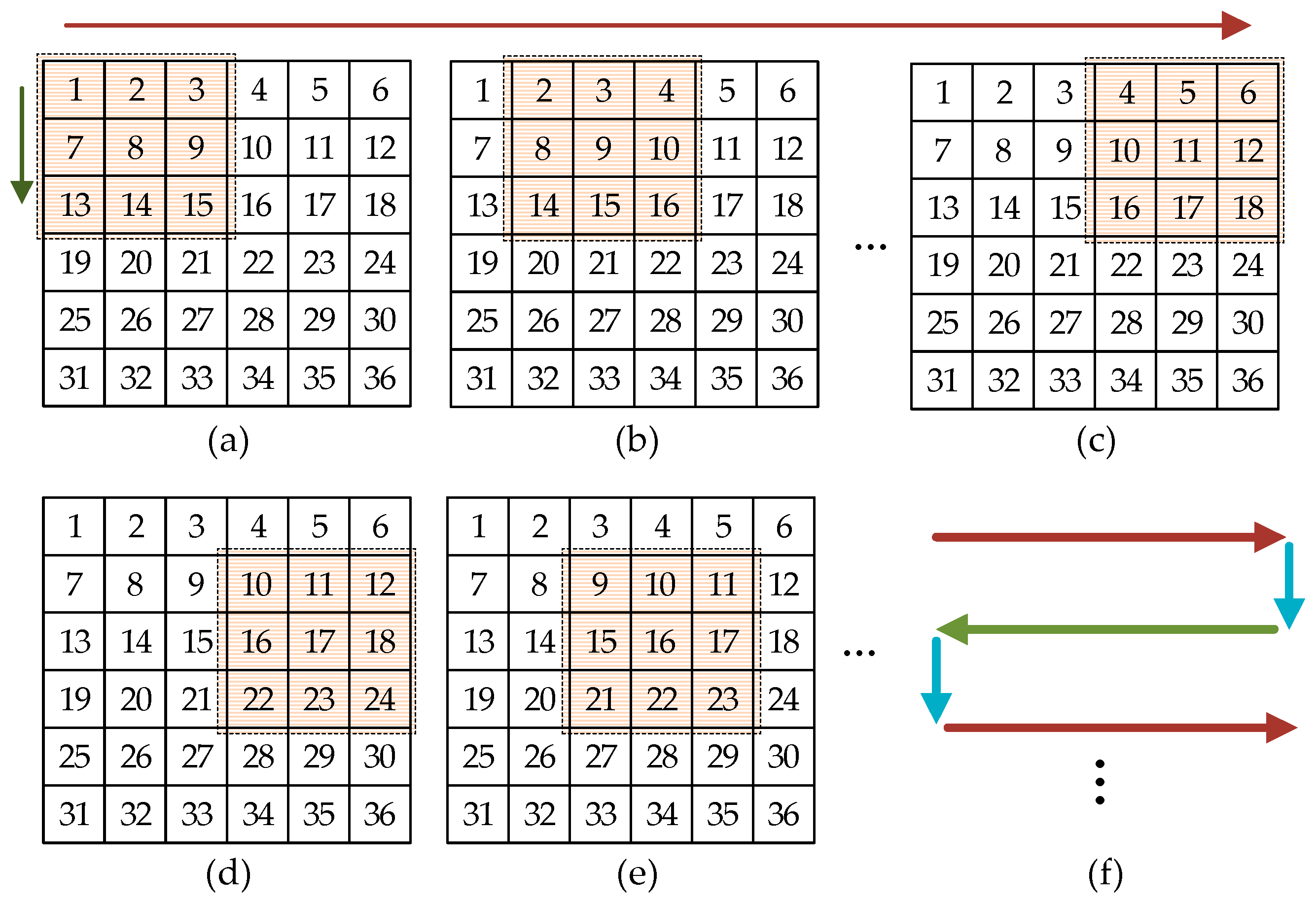
The data loading unit in the 2-D convolution circuit is the key to reduce data bandwidth. The data loading unit is composed of an address generator and a buffer RAM. Taking a 6*6 matrix (N = 6) and a 3*3 convolution kernel (K = 3) as examples, the working process of the designed data loading unit is illustrated in Figure 2.
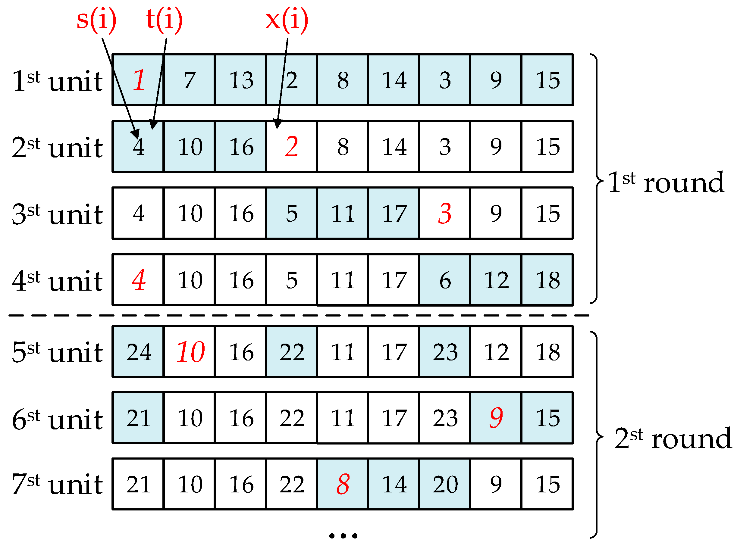
We define an operation between the submatrix extracted from the source matrix and the convolution kernel as a convolution unit. The operational data of each convolution unit is read from the source matrix in column-first order and the operations of each convolution unit are performed in left–right reciprocating order. Each scan of the convolution kernel from left to right or from right to left is called a round. Figure 2f illustrates this reciprocating data calculation order. This data loading method maximizes the data repeatability between adjacent convolution units, but the difficulty is in how to accurately retain the useful data in the previous convolution unit. This paper adopts a buffer RAM and designs a data loading strategy to solve this challenge. The workflow diagram of the data buffer RAM is shown in Figure 3.
The blue-filled boxes in Figure 3 are data that need to be read from the source matrix, while the red-marked italic data represent the start of data that are about to be sent to the MAC (Multiply Accumulate) unit for convolution calculation. It can be seen from Figure 3 that only three (which is equal to the kernel’s width K) data (missing) need to be loaded from the source matrix at a time when using the proposed reading strategy, which greatly reduces the bandwidth pressure of data RAM. The calculation methods of several key parameters in the structure are as follows.
The initial reading address of the ith convolution unit is expressed as x(i), and it is calculated by Equation (3).
x ( i ) = { [ x ( i 1 ) + K ] % K 2 o d d   r o u n d [ x ( i 1 ) K ] % K 2 e v e n   r o u n d [ x ( i 1 ) + 1 ] % K 2 1 s t   of   o d d   o r   e v e n   r o u n d
The starting address of replacement data is expressed as t(i), which can be calculated through x(i), and the equation is as follows:
t ( i ) = { [ x ( i ) + K ] % K 2 o d d   r o u n d   x ( i ) e v e n   r o u n d { x ( i 1 ) , x ( i 1 ) K , x ( i 1 ) 2 × K , x ( i 1 ) 3 × K } % K 2 1 s t   u n i t   o f   o d d   o r   e v e n   r o u n d
The starting reading address s(i) that needs to be read from source matrix for the next convolution unit data is calculated by Equation (5).
s ( i ) = { s ( i 1 ) + K × N + K 1 s ( i 1 ) + K × N s ( i 1 ) K × N + N 1 s ( i 1 ) K × N + N K s ( i 1 ) + 1 s ( i 1 ) 1 1 s t   u n i t   o f   t h e   o d d   r o u n d 1 s t   u n i t   o f   t h e   e v e n   r o u n d 2 s t   u n i t   o f   t h e   o d d   r o u n d 2 s t   u n i t   o f   t h e   e v e n   r o u n d o t h e r   u n i t s   o f   t h e   o d d   r o u n d o t h e r   u n i t s   o f   t h e   e v e n   r o u n d
Each time K new data is loaded from the source matrix (excluding the first convolution unit), the remaining K − 1 data can be calculated according to Equation (6) in turn after obtaining the starting reading address.
s ( i , j ) = { s ( i , j 1 ) + F s ( i , j 1 ) + 1   1 s t   u n i t   o f   t h e   o d d   o r   e v e n   r o u n d o t h e r   u n i t s 1 j K 1
To sum up, we read the data from the source matrix at the address computed by s(i), and fill them into the buffer RAM with t(i) as the starting position, then read K × K data from the buffer RAM starting with x(i) to perform convolution. The flow chart is shown in Figure 4.
Using this method, the number of data to be loaded from the source matrix can be calculated as follows:
[ ( N K + 1 ) 2 1 ] × K + K 2 = ( N K ) × ( N K + 2 ) × K + K 2
In conclusion, the bandwidth optimization rate when using this module to read data is:
η = 1 ( N K ) × ( N K + 2 ) × K + K 2 K 2 × ( N K + 1 ) 2
Taking the first level of the Alexnet network as an example, N is 224 and K is 11, hence, η is equal to 90.907%. Analogously, the optimization rate of the first layer in Lenet-5 is 66.591%.

2.3. Multifunctional Accumulation Unit

Since the multi-dimensional convolution in CNN is calculated by accumulating multiple 2-D convolutions, a vector adder is needed after the 2-D convolution unit. Meanwhile, in some networks, there exists a bias layer behind each convolution layer that provides a bias for the result of convolution. Since the bias unit works only after a convolution layer is fully completed, most of its time remains idle. Therefore, the bias unit and convolution accumulation unit share a data adder in our design, which we call an adder module in the following section.

2.4. Serial Max-Pooling Unit

The pooling circuit in CNN is used to down sample the convolution result that reduces the input data size of the subsequent network and accelerates the calculation of the neural network. The commonly used pooling methods are average pooling and max-pooling, in which average pooling includes accumulation and division calculation, so it is not suitable for hardware implementation. Therefore, we select max-pooling to act as our pooling method.
According to the principle of max-pooling, combined with the characteristics of data serial input, the designed serial pooling circuit consists of a selector, maximum comparator, pool controller, a previous result buffer and a line maximum buffer. The circuit structure is shown in Figure 5a.
The pooling circuit works in row order and stores the row pooling results in the max data buffer. When the next row is input, the pooling result of the corresponding pooling area of the previous row is read from the buffer and used to compare with the input data. Figure 5b illustrates how this pooling circuit works with an example.

3. CNN Accelerator Structure

3.1. Acceleration Chain Design

Due to the fact that the calculation sequence of CNN is relatively fixed, this paper constructs the CNN accelerator in the form of an acceleration chain, which reduces the data movement between the operations to obtain a higher performance. The acceleration module designed in Section 2 is connected by an on-chip stream bus to form an acceleration chain, and its structure is shown in Figure 6.
To enable the designed acceleration chain to finish a CNN network completely, a bypass control circuit is added to each module. When a module in the chain does not need to work in a certain layer, the specified module can be bypassed without affecting the calculation results and performance.
The accelerator designed in this paper adopts a fixed-point architecture. The determination of the data width of each calculation module in the acceleration chain is an important factor that needs to be prioritized. To maintain the accuracy of the operation, the data bit expansion operation is used inside each convolution layer, while the results are reduced by interception before the non-linear operation, so that the data widths between layers are consistent. The variation of data width in a chain is shown in Figure 7.
The M in Figure 6 is determined by the convolution kernel size supported by the accelerator circuit, and the formula is M = log2[K × K], while J is calculated by J = log2[Ln]. The maximum convolution kernel size supported by the accelerator in this paper is 11×11, and a convolution kernel can be connected to 16 input feature maps at most, so K = 11, Ln = 16, M = 7 and J = 4. Since the data bus width of the IoT system is usually 32 bits, in order to ensure that the psum of convolution with a width of 2Q + M + J can be stored in memory, the width of Q = (32 - M - J)/2 is restricted to 10 bits. Therefore, the accelerator we designed uses a 10-bit fixed-point architecture to complete the CNN calculation. To conclude, in each convolution layer, the operation mode of data width expansion is used, and the 32-bit operation temporary value psum is stored in the buffer storage. At the end of each convolution layer, the 32-bit operation data is reduced to 10 bits to ensure the consistency of data bit width between layers and to prevent data overflow caused by the increase of layers.
In order to evaluate the effect of the 10-bit data width on algorithm accuracy, we compared the accuracy of Lenet-5 and GoogleNet network under the data widths of float, int8, and int10 based on tensorflow, and the recognition accuracy is shown in Table 1.
As is widely accepted, the fixed point of data has little impact on the accuracy of CNN, and the resources saved for this can greatly benefit the IoT system.

3.2. Accelerator Structure Design

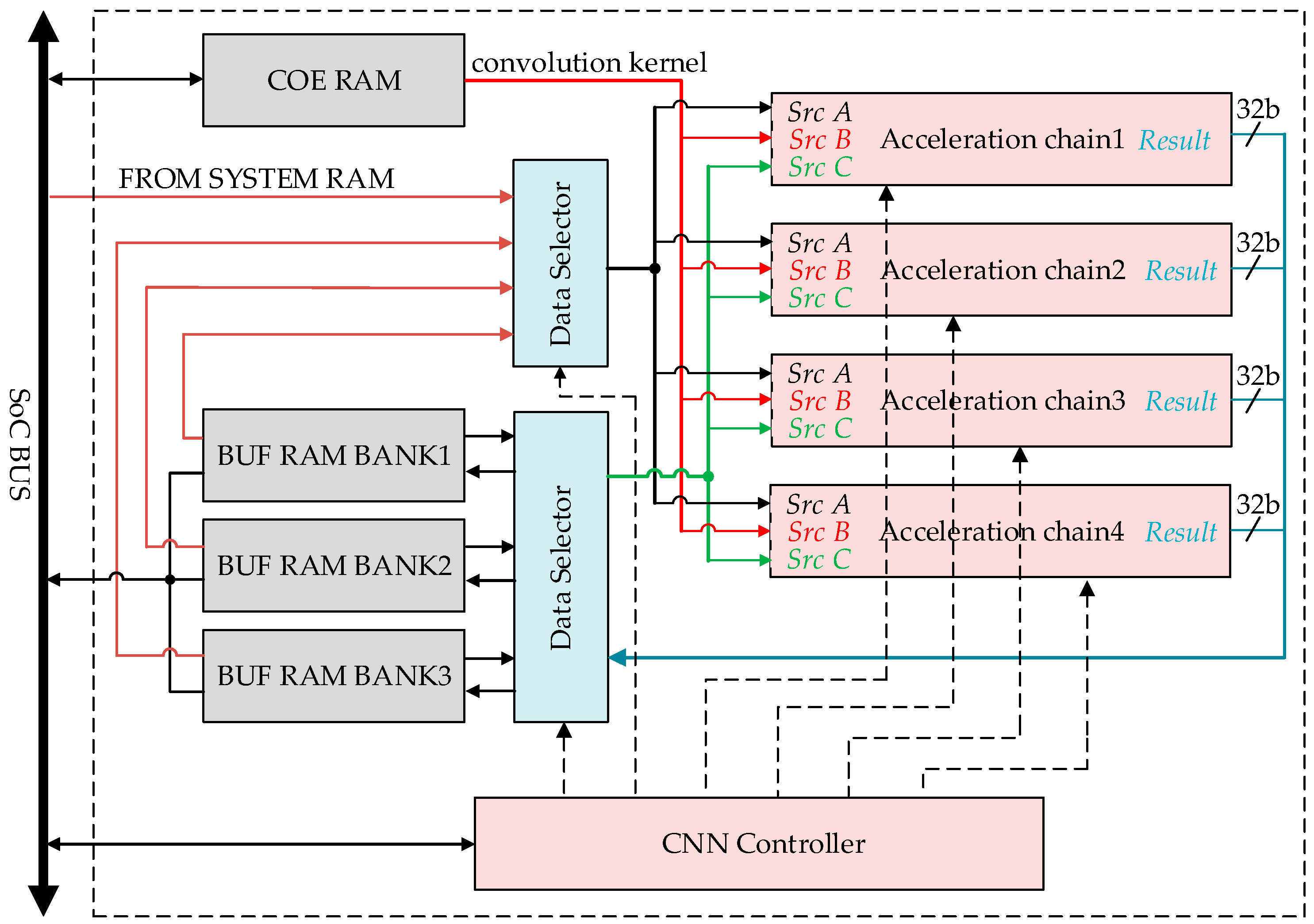
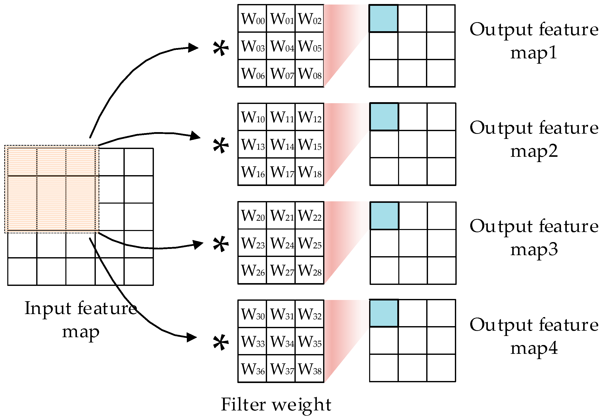
The structure of the compact CNN accelerator designed for the IoT endpoint SoC is shown in Figure 8. The accelerator consists of a CNN controller, three buffer blocks, four acceleration chains and data selectors. By using these modules, the designed accelerator can complete convolution, activation and subsampling operations with four convolution kernels simultaneously based on the use of the source matrix, as in Figure 9.
For each acceleration chain, there are four data channels: Src A, Src B, Src C and Result. According to the parallel method of source data sharing, the four acceleration chains share one Src A data channel, so there are 13 data channels in total. It can be seen from the designed structure that the Src B data are provided by the independent COE RAM and the remaining four Src C channels, four Result channels and one Src A channel are all connected to the BUF RAM BANK. Furthermore, for each BUF RAM BANK, an SoC access channel should also be included so that the calculation results can be read by the processor kernel.
The system contains three BUF RAM BANKs, and each of them has four access channels: SoC access channel, Src A read channel, Src C read channel and Result channel. Three banks alternately act as psum memory, source matrix memory, and result buffer memory. An example of the role changes during the working process is shown in Figure 10.
The result of the previous convolution calculation which can be called psum is read as the accumulated value of the next convolution. Furthermore, the BUF RAM BANK that saves the calculation results of each layer acts as the source data RAM of the next convolution layer. This design utilizes the data relationship between operations and layers, reduces the amount of data migration, improves the system performance and reduces power consumption.
Each BUF RAM BANK is spliced using four independent SP-RAMs to increase the access bandwidth and its structure is shown in Figure 11. For Result and Src C channels, each SP-RAM is independently addressed, while for the SoC access channel and source data access channel the SP-RAMs are uniformly addressed. A fixed priority arbitrator is designed for each SP-RAM to meet the time-sharing access requirements of the four interfaces. According to the importance of the data channel, the order of priority is Result, Src C, Src A, and SoC interface.
In conclusion, the basic parameters of the accelerator designed in this paper are shown in Table 2. The maximum input image supported by this accelerator is 256 × 256 and the maximum convolution kernel is 11 × 11, which can meet the general image recognition requirements of the IoT endpoint SoC. In addition, the accelerator can only use the convolution or pooling function to accelerate the traditional image processing algorithm and then meet the diverse task requirements of the IoT node processors.

4. Verification Platform Construction

We use the FPGA to verify the prototype of the CNN accelerator. By constructing an IoT node SoC and running an example network, we can more intuitively verify the functions and some performance characteristics of the designed accelerator.

4.1. Design of the Verification Platform Based on Cortex-M3

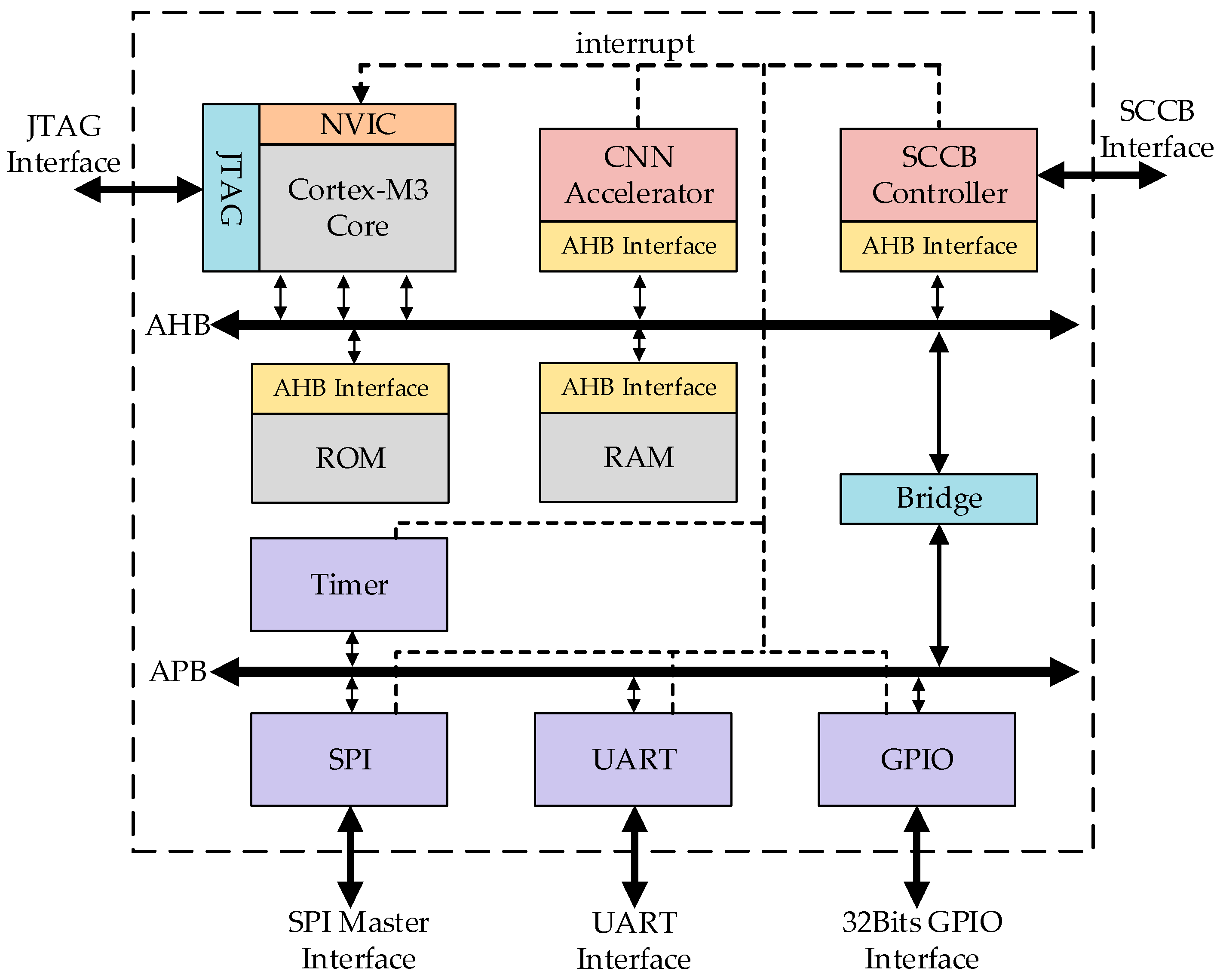
As an MCU kernel launched by ARM, Cortex-M3 (CM3) adopts Armv7-M Harvard architecture with a 3-stage pipeline, which makes it achieve a good balance between power and performance. The Dhrystone score of the CM3 kernel is 1.25 DMIPS/MHz (if simultaneous compilation is permitted, i.e., 1.89 DMIPS/MHz), which can meet the processing requirement of the IoT node devices [15]. Based on the Cortex-M3 kernel RTL netlist provided by the ARM Designstart project, we built a testing SoC to complete the functional verification and performance analysis of the designed CNN accelerator. The architecture of the SoC is shown in Figure 12.
The SoC built includes basic modules such as 128 KB RAM, 128 KB ROM and common peripherals such as GPIO and UART. As a processor core developed by ARM for an early time, Cortex-M3 uses AHB bus as its external interface, thus AHB (Advanced High performance Bus) and APB (Advanced Peripheral Bus) are used as the interconnected buses for the SoC, where high-speed devices such as SCCB (Serial Camera Control Bus) and CNN accelerators are connected with the kernel through AHB bus and low-speed devices such as GPIO are bridged through the APB bus.
We synthesize and implement the verification SoC on the FPGA, and obtain the resource report, as shown in Table 3. Figure 13 shows the breakdown of LUT resources for each circuit.

4.2. Implementation of the Lenet-5 Network in Verification SoC

The Lenet-5 proposed in 1994 is considered to be one of the earliest and most classical convolution neural networks. With the development of CNN research, a series of more effective CNN structures have been put forward but as a classical structure, Lenet-5 and its variants are still used to evaluate the performance of CNN accelerators [16].
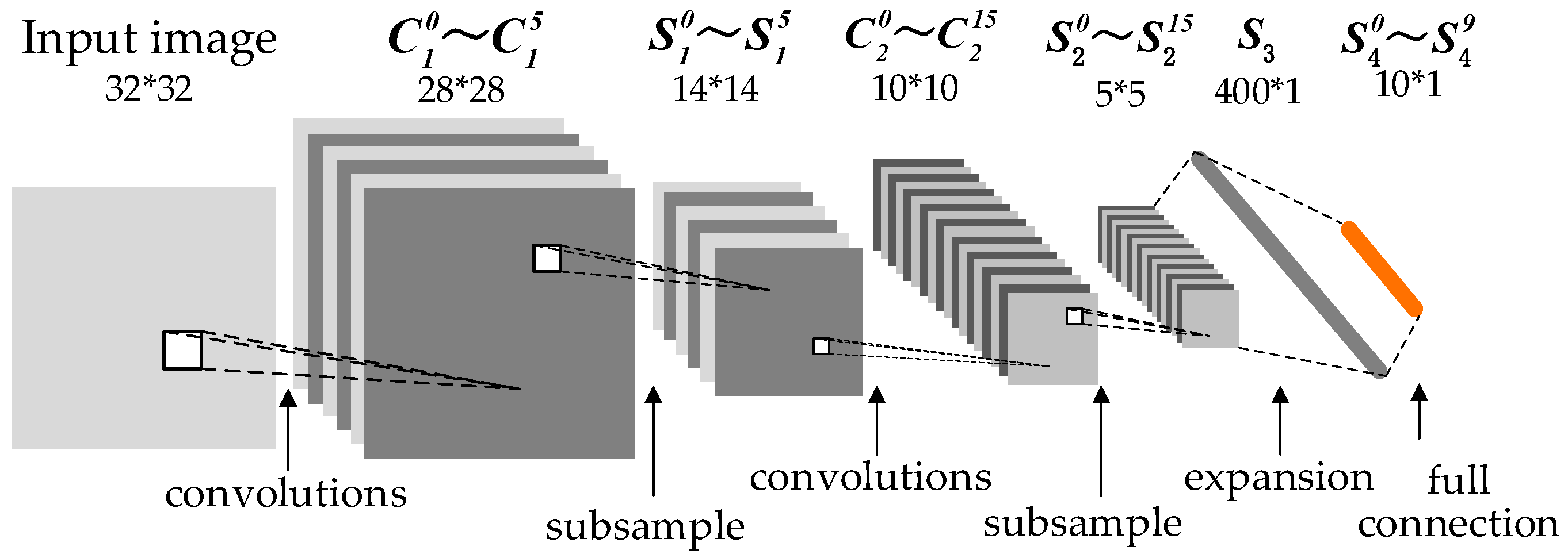
The structure of a Lenet-5 variant (abbreviated as Lenet-5) is shown in Figure 14. Its structure is divided into five hidden layers, which are the convolution layer with six convolution kernels, a subsampling layer S1, a partially connected layer containing sixteen convolution kernels, a subsampling layer S2, and a fully connected layer. More information about the Lenet-5 structure can be found in [17].
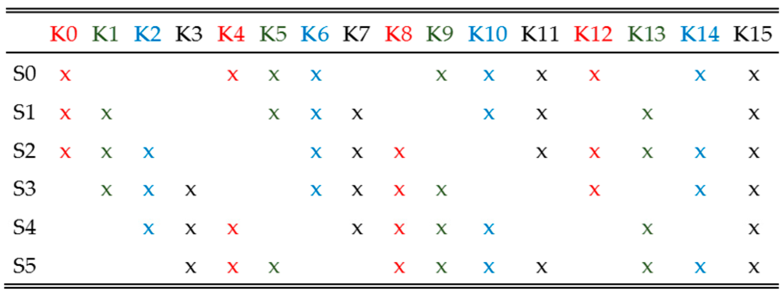
In Lenet-5, the calculation of the partially connected layer is the most complicated part because the results of this layer are related to the multiple layers or all outputs of the previous layer, so we mainly focus on the implementation of that layer. The specific connection relationship of the partially connected layer is shown in Figure 15.
The accelerator designed in this paper uses the method of reusing the input feature that maps to calculate the partial connection layer, i.e., calculating the connection between each input feature map and all convolution kernels by taking the input feature map as an order and storing the results in a BUFFER RAM BANK as psum. Since there are four acceleration chains in the accelerator, the 2-D convolution of each feature map and four convolution kernels can be calculated simultaneously. Among them, the first chain is responsible for calculating the connection with {K0, K4, K8, K12} and the second chain is responsible for calculating the connection with {K1, K5, K9, K13} and so on. Figure 16 illustrates this calculation process visually.
Through the analysis of the structure of the Lenet-5 network using the accelerator designed in this paper to complete the Lenet-5, the concrete realization process can be segmented into four steps as Table 4.

5. Evaluation and Results

5.1. Performance Analysis of the Accelerator

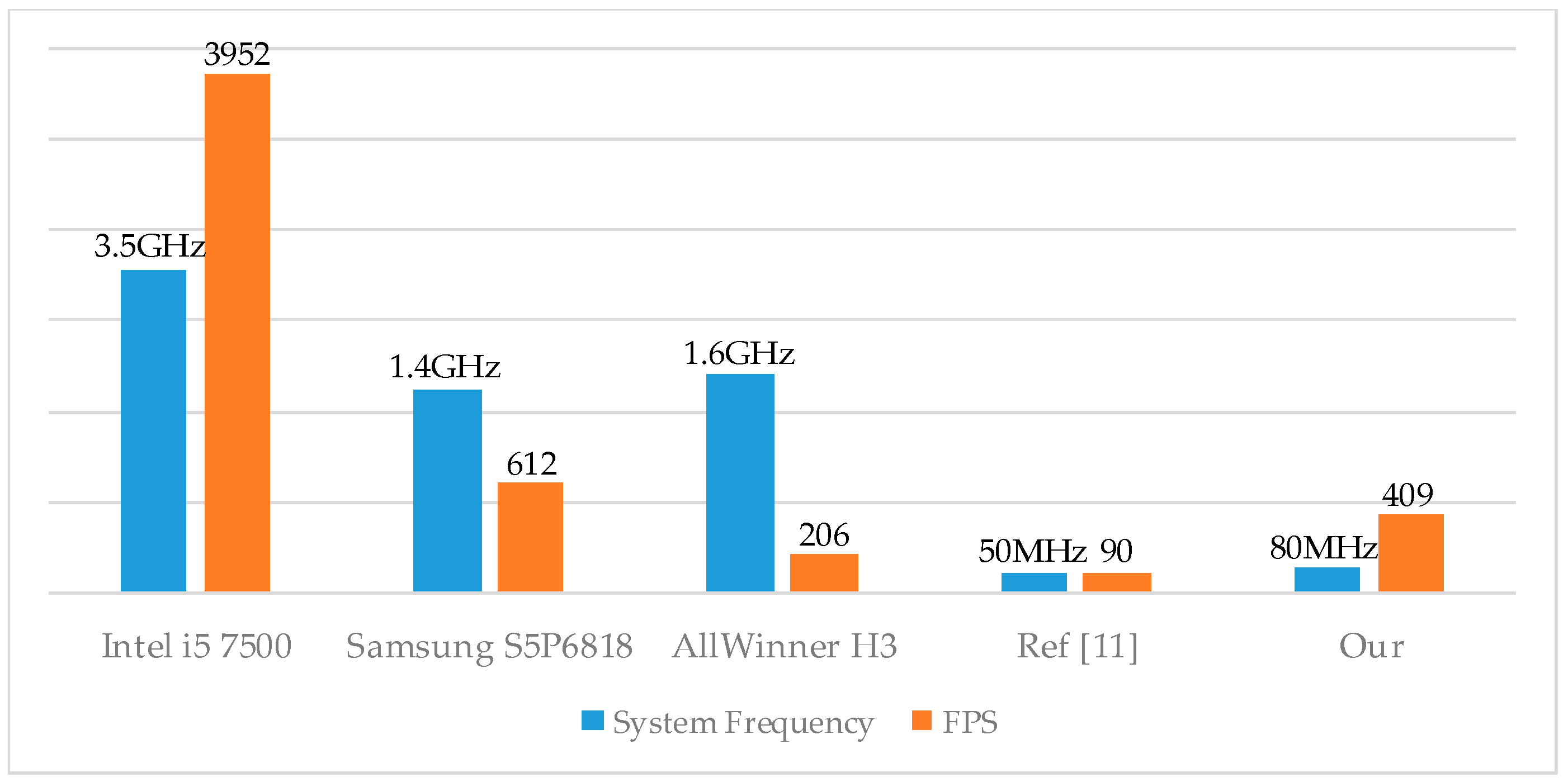
To evaluate the performance of the proposed architecture, we chose a desktop processor and two mobile application processors as performance evaluation objects. In order to estimate the execution time of the Lenet-5 network on different hardware and software platforms, we used C language to implement forward propagation of Lenet-5. The forward propagation program of Lenet-5 was run on Intel 7500, Samsung S5P6818 and AllWinner H3 to compare with the SoC designed in this paper, respectively. The execution time of each platform is listed in Table 5 and Figure 17, in which frame pre-second (FPS) denotes how many MNIST figures (the size of the figures in the data set is 32 × 32) can be processed in one second.

5.2. Analysis of Resource Consumption

To design a CNN accelerator suitable for IoT systems, compact structure is a key principle during the design process. In order to complete the evaluation of resource consumption of the accelerating module, we have implemented our designed circuit on FPGA. The model of the FPGA board is Xilinx VC707 (XC7VX485T-2) (Xilinx, San Jose, CA, USA) and the synthesize tool is Vivado 17.2. The resource consumption comparison between the designed module in this paper and the reference [11,18,19] is shown in Table 6.
Considering that the target application scenario of this paper is in resource-constrained IoT node SoC, the cost and area of these chips may only be equivalent to STM32 or ESP32. It is impractical to rely on a large number of hardware multipliers to improve computing throughput, as high-performance multipliers that occupy a large number of circuit areas and dynamic power consumption are very rare resources in IoT chips.
The accelerator proposed in this paper takes up less than one-third of the resources than in [18] and exceeds its computational power. Although this accelerator cannot compete with some high-performance accelerators such as the one proposed in [19], or some GPU in performance, the resource and power consumption are less than 10% of these chips, which meets the need of the IoT node SoC to implement basic CNN computing with a compact structure and low cost. Since the computation of the Tiny-Yolo V2 network is 6.97 GOPS, while that of the Squeezenet network is only 0.86 GOPS, the accelerator designed in this paper can meet the calculation requirements of these networks. For many IoT nodes such as wearable devices, power consumption and chip area are often more attractive than redundant performance.
In order to evaluate the resource and power consumption characteristics of the designed accelerator more accurately, we will use IC design tools to synthesize the circuit after modifying the accelerator IP in our future work. Meanwhile, we will use the prototype verification system designed to develop some practical IoT applications, such as face detection, face recognition, and license plate recognition.

6. Conclusions

In this paper, a compact and efficient convolutional neural network accelerator for IoT endpoint SoC is proposed. Firstly, we propose a convolution calculation method that uses repeatability of convolution data to reduce data bandwidth usage and designs function circuits such as convolution, accumulation and pooling. Secondly, we use these modules to form a compact multi-function accelerator and design an efficient storage method for the accelerator. Thirdly, a verification SoC is implemented on the Xilinx VC707 FPGA based on the Cortex-M3 kernel. Finally, the evaluation of the designed accelerator is achieved by migrating the Lenet-5 network on the verification platform and comparing with other platforms.
This paper designs a verification SoC based on the Cortex-M3 kernel and uses the Lenet-5 network and MINIST as test cases to evaluate the performance of the accelerator. We select a desktop CPU and two mobile application processors which are typical high-performance IoT SoC as reference objects for performance comparison. The test results show that the proposed accelerator can make the computing power of the Cortex-M3 kernel, with a main frequency of only 80 MHz, nearly two times higher than that of quad-core Cortex-A7 SoC and 67% of the computational power of eight-core Cortex-A53 SoC Samsung S5P6818. Accelerator throughput is about 6.54 GOPS at a 220 MHz frequency with a circuit cost of only 4901 LUTs and it does not use precious hardware multiplier resources, which can meet the needs of AI computing of the endpoint SoC for the IoT.

Author Contributions

Conception and structure of the concept of this paper, F.G.; Resources, F.Z. and H.X.; Supervision, N.W.; Writing-original draft, F.G.; Writing-review and editing, Y.Z., and H.X.

Funding

This work was supported by National Natural Science Foundation of China (No. 61774086), Natural Science Foundation of Jiangsu Province (No. BK20160806), the Fundamental Research Funds for Central Universities (No. NP2019102), Project of Science and Technology on Electronic Information Control Laboratory.

Acknowledgments

The authors would like to thank Muhammad Rehan Yahya for his beneficial suggestions and comments.

Conflicts of Interest

The authors declare no conflict of interest.

References

  1. Samie, F.; Bauer, L.; Henkel, J. From Cloud Down to Things: An Overview of Machine Learning in Internet of Things. IEEE Internet Things J. 2019, 4662, 1. [Google Scholar] [CrossRef]
  2. Yamakami, T. An Experimental Implementation of an Edge-based AI Engine with Edge-Cloud Coordination. In Proceedings of the ISCIT 2018—18th International Symposium on Communication and Information Technology, Bangkok, Thailand, 26–29 September 2018. [Google Scholar]
  3. Du, Y.; Du, L.; Li, Y.; Su, J.; Chang, M.F. A Streaming Accelerator for Deep Convolutional Neural Networks with Image and Feature Decomposition for Resource-limited System Applications. arXiv arXiv:1709.05116. Available online: https://arxiv.org/abs/1709.05116 (accessed on 10 February 2019).
  4. Liu, B.; Zou, D.; Feng, L.; Feng, S.; Fu, P.; Li, J. An FPGA-Based CNN Accelerator Integrating Depthwise Separable Convolution. Electronics 2019, 8, 281. [Google Scholar] [CrossRef]
  5. Sainath, T.N.; Kingsbury, B.; Saon, G.; Soltau, H.; Mohamed, A.R.; Dahl, G.; Ramabhadran, B. Deep Convolutional Neural Networks for Large-scale Speech Tasks. Neural Networks 2015, 64, 39–48. [Google Scholar] [CrossRef] [PubMed]
  6. Zhang, C.; Li, P.; Sun, G.; Guan, Y.; Xiao, B.; Cong, J. Optimizing FPGA-based Accelerator Design for Deep Convolutional Neural Networks. In Proceedings of the 2015 ACM/SIGDA International Symposium on Field-Programmable Gate Arrays, Monterey, CA, USA, 22–24 February 2015; pp. 161–170. [Google Scholar]
  7. Han, S.; Mao, H.; Dally, W.J. Deep Compression: Compressing Deep Neural Networks with Pruning, Trained Quantization and Huffman Coding. 2015, pp. 1–14. Available online: https://arxiv.org/abs/1510.00149 (accessed on 15 October 2018).
  8. Cavigelli, L.; Benini, L. Origami: A 803-GOp/s/W Convolutional Network Accelerator. IEEE Trans. Circuits Syst. Video Technol. 2017, 27, 2461–2475. [Google Scholar] [CrossRef] [Green Version]
  9. Chen, Y.-H.; Krishna, T.; Emer, J.; Sze, V. Eyeriss JSSC 2017: An energy-efficient reconfigurable accelerator for deep convolutional neural networks. IEEE J. Solid-State Circuits 2017, 52, 127–138. [Google Scholar] [CrossRef]
  10. Conti, F.; Schilling, R.; Schiavone, P.D.; Pullini, A.; Rossi, D.; Gurkaynak, F.K.; Muehlberghuber, M.; Gautschi, M.; Loi, I.; Haugou, G.; et al. An IoT Endpoint System-on-Chip for Secure and Energy-Efficient Near-Sensor Analytics. IEEE Trans. Circuits Syst. I Regul. Pap. 2017, 64, 2481–2494. [Google Scholar] [CrossRef] [Green Version]
  11. Zhang, Y.; Wu, N.; Zhou, F.; Yahya, M.R. Design of Multifunctional Convolutional Neural Network Accelerator for IoT Endpoint SoC. In Proceedings of the World Congress on Engineering and Computer Science 2018, San Francisco, CA, USA, 23–25 October 2018; pp. 16–19. [Google Scholar]
  12. Jacob, B.; Kligys, S.; Chen, B.; Zhu, M.; Tang, M.; Howard, A.; Adam, H.; Kalenichenko, D. Quantization and Training of Neural Networks for Efficient Integer-Arithmetic-Only Inference. In Proceedings of the IEEE Computer Society Conference on Computer Vision and Pattern Recognition, Salt Lake City, UT, USA, 18–22 June 2018; pp. 2704–2713. [Google Scholar]
  13. Zhang, M.; Li, L.; Wang, H.; Liu, Y.; Qin, H.; Zhao, W. Optimized Compression for Implementing Convolutional Neural Networks on FPGA. Electronics 2019, 8, 295. [Google Scholar] [CrossRef]
  14. Hegde, K.; Yu, J.; Agrawal, R.; Yan, M.; Pellauer, M.; Fletcher, C.W. UCNN: Exploiting computational reuse in deep neural networks via weight repetition. In Proceedings of the 45th Annual International Symposium on Computer Architecture (ISCA), Los Angeles, CA, USA, 2–6 June 2018; pp. 674–687. [Google Scholar]
  15. ARM. ARM Cortex-M3 Processor Technical Reference Manual; ARM Limited Company: Cambridge, UK, 2015; pp. 1–121. [Google Scholar]
  16. Du, L.; Du, Y.; Li, Y.; Su, J.; Kuan, Y.-C.; Liu, C.-C.; Chang, M.-C.F. A Reconfigurable Streaming Deep Convolutional Neural Network Accelerator for Internet of Things. IEEE Trans. Circuits Syst. I Regul. Pap. 2017, 65, 198–208. [Google Scholar] [CrossRef]
  17. LeCun, Y.; Bottou, L.; Bengio, Y.; Haffner, P. Gradient-based learning applied to document recognition. Proc. IEEE 1998, 86, 2278–2323. [Google Scholar] [CrossRef]
  18. Li, Z.; Wang, L.; Guo, S.; Deng, Y.; Dou, Q.; Zhou, H.; Lu, W. Laius: An 8-bit fixed-point CNN hardware inference engine. In Proceedings of the 2017 IEEE International Symposium on Parallel and Distributed Processing with Applications and 2017 IEEE International Conference on Ubiquitous Computing and Communications (ISPA/IUCC), Guangzhou, China, 12–15 December 2017; pp. 143–150. [Google Scholar]
  19. Guo, K.; Sui, L.; Qiu, J.; Yu, J.; Wang, J.; Yao, S.; Han, S.; Wang, Y.; Yang, H. Angel-Eye: A complete design flow for mapping CNN onto embedded FPGA. IEEE Trans. Comput. Des. Integr. Circuits Syst. 2018, 37, 35–47. [Google Scholar] [CrossRef]
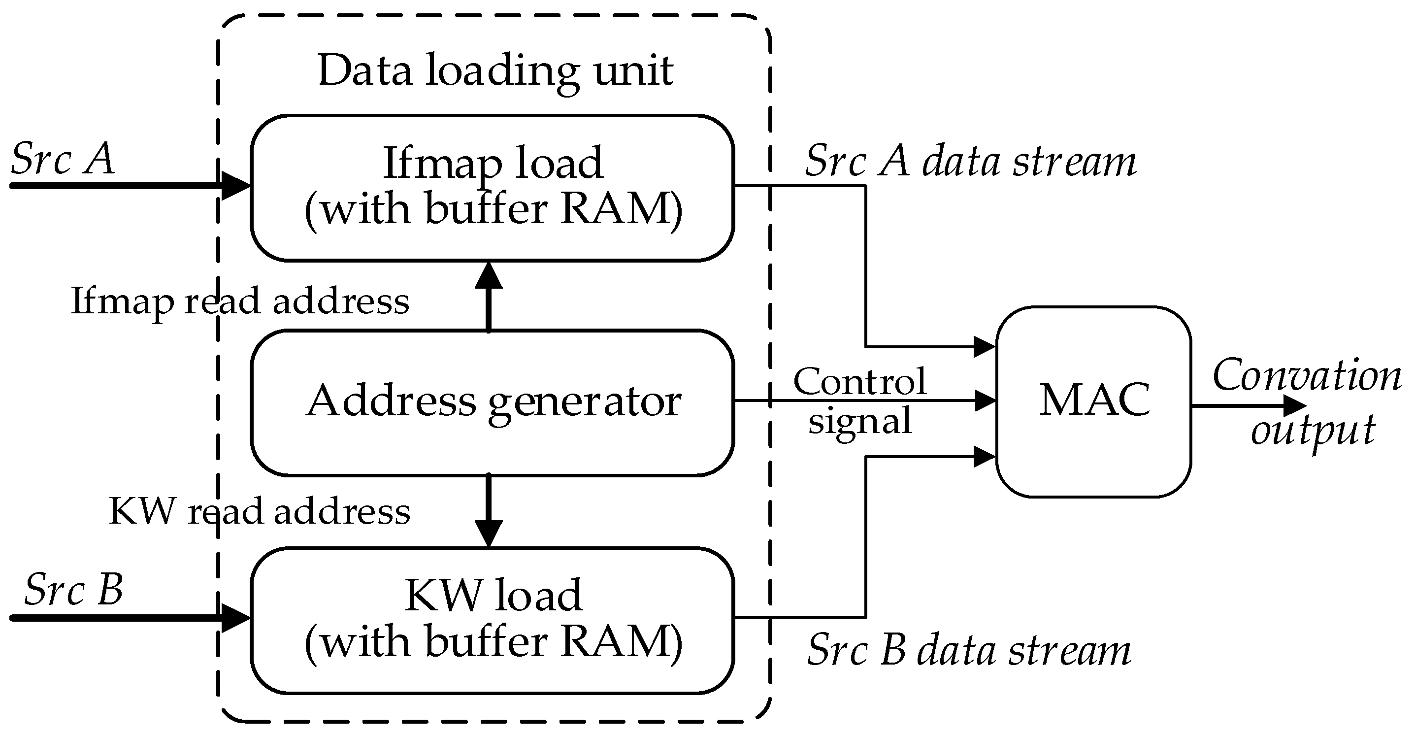
Figure 1. Convolution circuit structure diagram.
Electronics 08 00497 g001
Figure 2. (a~e) Demonstration of a 2-D convolution workflow. (f) Convolution unit operation order.
Electronics 08 00497 g002
Figure 3. Demonstration of the convolution data buffer RAM workflow.
Electronics 08 00497 g003
Figure 4. Flow chart of the convolutional data loading.
Electronics 08 00497 g004
Figure 5. (a) Max-pooling circuit structure. (b) Example of a pooling circuit.
Electronics 08 00497 g005
Figure 6. Schematic diagram of the acceleration chain.
Electronics 08 00497 g006
Figure 7. Data width variation in the acceleration chain.
Electronics 08 00497 g007
Figure 8. Architecture of the accelerator.
Electronics 08 00497 g008
Figure 9. Schematic diagram of calculation based on source data sharing.
Electronics 08 00497 g009
Figure 10. Function conversion diagram of three BUF RAM BANK modules.
Electronics 08 00497 g010
Figure 11. Function conversion diagram of three BUF RAM modules.
Electronics 08 00497 g011
Figure 12. SoC structure based on CM3.
Electronics 08 00497 g012
Figure 13. The proportion of resources used by SoC modules.
Electronics 08 00497 g013
Figure 14. The structure of a Lenet-5 network.
Electronics 08 00497 g014
Figure 15. Connection relations of partial connection layers in Lenet-5.
Electronics 08 00497 g015
Figure 16. Schematic flow chart of partial connection layer.
Electronics 08 00497 g016
Figure 17. Acceleration performance comparison of the CNN accelerator.
Electronics 08 00497 g017
Table 1. The effect of data width on network accuracy.
FloatInt8 Int10
Lenet-595.18%95.11%95.15%
GoogleNet89.10%87.53%88.83%
Table 2. Accelerator performance summary.
ParameterDescription
Precision10-bit fixed-point
Feature map size(1~256)*(1~256)
Kernel size(1~11)*(1~11)
Pool typemax pool
Pool size1~8
Parallelism1~4
Function
(Arbitrary combination)
convolution (1-D or 2-D)
data add (matrix or bias)
pooling
ReLU activation
Table 3. SoC LUT Resource Consumption.
Cortex-M3 KernelAHB Bus APB BusPeripheralsAccelerator
LUT1516226011912384901
Table 4. The computation process of Lenet-5 using the accelerator.
LayerCalculation MethodsDescription
C1 & S1 [ S 1 0 ~ S 1 5 ] = p o o l [ r e l u [ S * [ K 1 0 ~ K 1 5 ] ] ] Convolution and subsampling
C2 & S2 [ S 2 0 ~ S 2 15 ] = S 1 0 * [ K 2 0 ~ K 2 15 ]
[ S 2 0 ~ S 2 15 ] = S 1 1 * [ K 2 0 ~ K 2 15 ] + [ S 2 0 ~ S 2 15 ]

[ S 2 0 ~ S 2 15 ] = p o o l [ r e l u [ S 1 15 * [ K 2 0 ~ K 2 15 ] + [ S 2 0 ~ S 2 15 ] ]
Partially connection and subsampling
S3 S 3 = [ S 2 0 ~ S 2 15 ] Expansion
S4 [ S 4 0 ~ S 4 9 ] = S 3 * [ K 3 0 ~ K 3 9 ] Full connection
Table 5. Acceleration performance table.
SoCArchitectureCore NumberFrequencyLatency/Image Frame Per Second
Intel i5 7500Kaby Lake43.5 GHz0.253 ms3952
Samsung S5P6818Cortex-A5381.4 GHz1.633 ms612
AllWinner H3Cortex-A741.6 GHz4.852 ms206
ProposedCortex-M3180 MHz2.44 ms409
Table 6. Accelerator resource consumption and performance comparison table.
LUTFFBRAMDSPThroughputPower/W
Proposed490129834806.54 GOPS @220 MHz0.380
[11]5717620739201.602 GOPS @153 MHz0.370
[18]1528520745715645.2 GOPS0.607
[19]298673548985.5190137 GOPS @150 MHz9.630