Article

Towards Silicon Carbide VLSI Circuits for Extreme Environment Applications

Division of Electronics, KTH Royal Institute of Technology, 164 40 Stockholm, Sweden
*
Author to whom correspondence should be addressed.
Electronics 2019, 8(5), 496; https://doi.org/10.3390/electronics8050496
Submission received: 14 March 2019 / Revised: 14 April 2019 / Accepted: 26 April 2019 / Published: 3 May 2019
(This article belongs to the Section Microelectronics)

Abstract

:
A Process Design Kit (PDK) has been developed to realize complex integrated circuits in Silicon Carbide (SiC) bipolar low-power technology. The PDK development process included basic device modeling, and design of gate library and parameterized cells. A transistor–transistor logic (TTL)-based PDK gate library design will also be discussed with delay, power, noise margin, and fan-out as main design criterion to tolerate the threshold voltage shift, beta ( β ) and collector current ( I C ) variation of SiC devices as temperature increases. The PDK-based complex digital ICs design flow based on layout, physical verification, and in-house fabrication process will also be demonstrated. Both combinational and sequential circuits have been designed, such as a 720-device ALU and a 520-device 4 bit counter. All the integrated circuits and devices are fully characterized up to 500 °C. The inverter and a D-type flip-flop (DFF) are characterized as benchmark standard cells. The proposed work is a key step towards SiC-based very large-scale integrated (VLSI) circuits implementation for high-temperature applications.

1. Introduction

Electronics for the high-temperature (HT) ambient without cooling are promising for many application areas such as aeronautics, deep-well drilling and automation [1,2]. Silicon Carbide (SiC)-based integrated circuits (IC) are potentially capable of sustained operation at extreme temperature, because of the wide band gap (3.2 eV) [3,4]. Progress towards SiC-based very large-scale integrated (VLSI) circuits such as HT microcontrollers would enable systems with digitally controlled sensors and actuators. A process design kit (PDK) for VLSI circuits functional at elevated-temperature opens many new opportunities.
Raytheon UK has facilitated this need and developed a minimum featured size of 1.2 μ m SiC complementary metal-oxide-semiconductor (CMOS) process called HiTSiC [5]. This MOSFET technology, which has a gate oxide that could cause reliability issues [6,7], is not an ideal candidate, in particular, for HT applications. However, using this process, Raytheon has successfully demonstrated circuits to be operational up to 400 °C. Later, the University of Arkansas with the collaboration of Ozark Integrated Circuits Inc. has developed a SiC CMOS PDK [8], which includes transistor models, parameterized cells (P-cells) and design rules. The PDK was demonstrated using a library of standard digital cell using two example parts; an 8-bit register and a programmable delay line operational at 300 °C [9].
SiC ICs based on junction field-effect transistor (JFET), measured at temperatures exceeding 800 °C, were reported in [10], including an inverter-based 26-transistor 11-stage ring oscillator; however, bipolar junction transistors (BJTs) have better driving capability and linearity and higher speed as compared to FETs [11]. Digital and analog ICs realized in bipolar SiC technology using emitter-coupled logic (ECL) have previously been demonstrated up to 500 °C [11,12,13,14], with a noise margin of 1 V [12]. An active down-conversion mixer realized using 4H-SiC BJT, for communication receivers, was recently reported working up to 500 °C [15].
This paper reports a PDK and set of reference ICs implemented in SiC bipolar low-power process by employing transistor–transistor logic (TTL) [16] as a proof of concept that can be extended to implement more complex SiC ICs. Standard cell area plays a dominant role when it comes to integrating complex integrated circuits and systems, and TTL based standard cells can be extended for multiple inputs with less area overhead (e.g., To make 3-input from a 2-input NAND, one need to add only one emitter finger at the input transistor. No more transistors are needed.) [16]. Because of good logic swing and noise margin, TTL-based SiC ICs provide a stable operation at HT. Recently our group reported SiC TTL-based ring-oscillator characterized up to 600 °C [17] and a TTL 2-input NAND gate working up to 500 °C [18]. For a monolithic more complex SiC bipolar ICs design, integration, physical implementation and fabrication a PDK is highly demanded. The PDK development process consisting of modeling basic devices, and designing gate/module library and parametrized cells will be discussed in this paper. The PDK based digital ICs design flow based on layout, physical verification, and in-house fabrication process will also be demonstrated here by set of combinational and sequential reference circuits. All the devices, gate/module library and reference ICs were fully characterized up to 500 °C. This work is an important step towards SiC-based application specific integrated circuits (ASICs) implementation.
The paper is organized as follows. Section 2 describes the methodology of building a PDK for a low-voltage bipolar digital IC technology and design, physical implementation and fabrication using the established PDK. Section 3 presents the results of devices, gate/module library, and combinational and sequential reference circuits. Discussion and conclusions are presented in Section 4 and Section 5 respectively.

2. Methodology

The main goal of this work was to explore and demonstrate the feasibility of monolithic SiC bipolar integrated circuits for HT applications. The design and in-house process implementation of the digital ICs were carried out in two phases. First, building a process design kit for the in-house SiC bipolar technology. Secondly, working with the PDK in SiC digital ICs design by employing a top-down approach.

2.1. Development of Process Design Kit

For the SiC VLSI circuits implementation the circuits building blocks have been designed to facilitate precise digital, analog and mixed-signal interface electronics for extreme environments. A Process Design Kit (PDK) is needed to design such circuits. A flowchart summarizing the PDK building process for the SiC bipolar low-voltage technology is shown in Figure 1. The SiC TTL PDK includes transistor and resistor models, design rules, routing verification checks, basic devices parametrized cells (P-cells), gate/module library, and standard cells library.

2.1.1. Gate Library (Gate Transistor Level Schematic Design)

The PDK gates schematic design in 4H-SiC bipolar low-voltage IC technology is based on the simple and robust TTL family available in literature [16]. The high-temperature operation of SiC devices causes electrical properties variation and produce noise in the SiC-based ICs. Therefore the noise margins are selected as the main design parameter and they are also an important figure of merit for digital circuits. The TTL-based gates schematics have been designed by specifying circuit parameters to provide adequate noise margins and stable voltage levels at HT operations. The SiC TTL-based gate design for fan-out, noise margins, and propagation delay is discussed in Section 3.2. The PDK gate library was implemented in Cadence Virtuoso ADE. The TTL-based gate/module reported in this paper are listed in Table 1, which are part of the PDK gate and module library.

2.1.2. Gate Library Simulations

The Spice Gummel-Poon (SGP) [19] and Vertical Bipolar Intercompany Model (VBIC) [20] were chosen for the high-temperature modeling. The SGP HT-models were developed [21] for binned temperature points (25 °C, 100 °C, 200 °C, 300 °C, 400 °C, 500 °C) for the device from a previous fabrication round by extracting the DC parameters from forward and reverse output characteristics as well as the Gummel plot of an n-p-n bipolar transistor. All the parameters of the HT models are provided in [21]. The HT models corresponding to desired temperature points can be setup in Cadence by choosing the model libraries. VBIC models were developed with continuous temperature scalability over a wide temperature range [22] but were not used in this work.

2.1.3. Standard Cell Layout Design and Library

A common entity of all ASIC PDKs is the standard cell, which is a layout using P-cells, mask layers and vias following the schematic topology. The P-cells give freedom to designer to enter a specific parameter for the devices like n-p-n bipolar transistor and get the multi-emitter transistor for a TTL implementation. The integrated resistors are also parametrized to set a specific length and hence the resistance.
The PDK consists of four different types of P-cells and corresponding mask layers and vias are shown in Figure 2. The PDK layers and vias are shown on the left hand side. The bipolar transistor circuit diode is made by shortening the base and collector terminals. The epitaxial integrated resistor has its width “W” fixed and the length “L” is parametrized to get the required resistance. The multi-emitter bipolar transistor P-cells configured as single-emitter, double-emitter, and triple-emitter are shown on the right hand side top-down respectively. An Inverter and 2-input NAND gates standard cell illustration using SiC TTL PDK are shown in Figure 3.

2.1.4. Physical Verification

After successful simulations at transistor level, using the Cadence Spectre simulator, standard cell, place and route was performed. In order to ensure the in-house standards (minimum spacing, minimum metal width, via placement, via dimensions, fixed standard cell height etc.) and correct signal and power routing, design rule check (DRC) and layout versus schematic (LVS) programs were programmed in the physical verification system (PVS) tool. After the successful place and route the GDSII file is generated to order the masks set and the next step is fabrication.

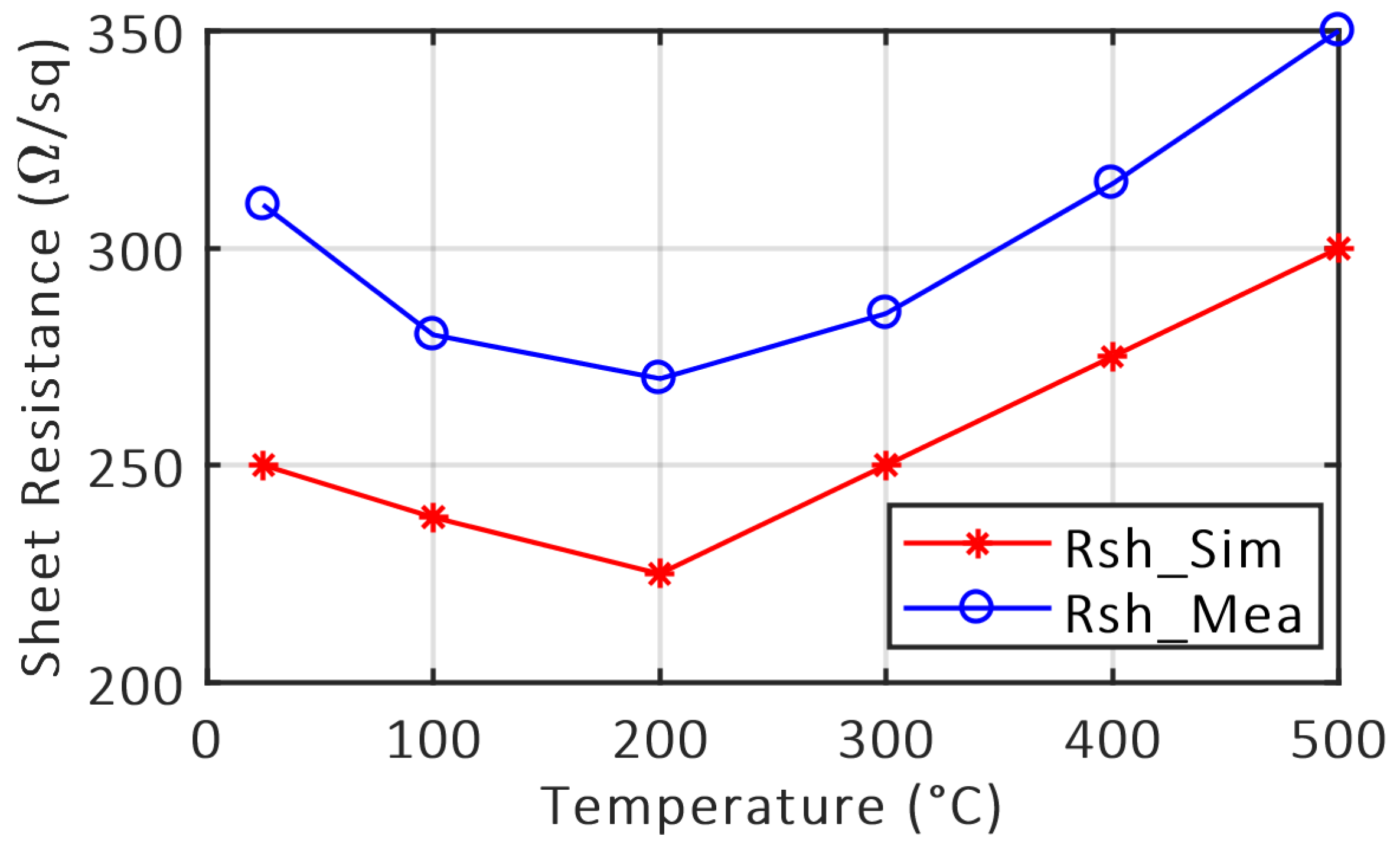
2.1.5. Test-structures HT Measurements and Modeling

Design of the PDK begins with the modeling and characterization of an NPN-bipolar transistor. The in-house SiC BJT low-voltage process technology optimization is described in [23]. The fabricated test structures are measured on the wafer using a hot-chuck probe-station, KEITHLEY SCS-4200 parameter analyzer, and Keysight parameter extraction and optimization software IC-CAP. The feedback provided by the characterization of the test structures were used for the model validation.

2.2. Digital ICs Realization with SiC TTL PDK

2.2.1. Digital Circuit Design

A digital IC realization in the in-house SiC bipolar process was carried out by employing a top-down approach (see Figure 4). The established PDK gate/module library has been used to implement a gate level design at SiC bipolar transistor level in Cadence Virtuoso IC design environment. After SiC TTL implementation of digital IC, the transistor level simulations are carried out using the high-temperature compact models.

2.2.2. Layout Implementation and Verification

After the successful transistor level simulations, the circuit layout implementation is carried out using the PDK standard cell library. The layout implementation of digital circuit is illustrated in Figure 5 using the PDK standard cells. In this example a 5-stage ring oscillator using 4 Inverters, 2-input NAND and a Buffer standard cells are implemented at layout and the implementation process can be extended to any digital circuit layout realization.

2.2.3. Fabrication

100 mm 4H-SiC N-type wafers were procured from Norstel AB (Norrköping, Sweden) for this study. The wafers had five epitaxial layers. A 2D cross-sectional view with the doping profile of all five layers and the micro-photograph of a fabricated n-p-n transistor is shown in Figure 6a,b respectively. After reactive ion etching of the emitter, base and isolation region, a sacrificial oxide was thermally grown in dry O2. The passivation oxide was made by plasma enhanced chemical vapor deposition (PECVD) of 100 nm SiO2 with post-deposition annealing. More details on the SiC low power fabrication process are reported in [17,23]. The circuits have two levels of interconnects. Each metal layer is sputtered 100 nm TiW and 2000 nm Al. The TiW serves as both an adhesion layer and a diffusion barrier between Al and Ohmic contacts. The thickness of an interconnect dielectric (PECVD SiO2) is 400 nm between SiC mesas to the 1st metal layer and 1000 nm between the 1st and 2nd metal layer. The minimum aspect ratio (width/height) of via was 4:1. The minimum spacing between metal lines was 4 μ m. The minimum width of the via was 4 μ m. The minimum width of the metal lines was 6 μ m.

2.2.4. Measurement Setup

The fabricated circuits were characterized on wafer by using a hot-chuck probe-station from 25 °C to 500 °C. The input signals were generated using an FPGA. The SiC TTL logic is characterized in a supply voltage range of 8 V to 20 V, the input stimulus signals levels are translated using commercial-off-the-shelf driver circuit CD40109B. The transient response is measured using KEYSIGHT InfiniiVision MSO-X 3024A mixed signal oscilloscope. The BJTs and gate DC measurements are carried out using KEITHLEY parameter analyzer (SCS4200). The measurement setup of SiC devices ICs is shown in Figure 7.

3. Results

The SiC TTL PDK has been successfully used in the design, implementation, and fabrication of monolithic SiC integrated circuits and devices in the in-house bipolar low-voltage technology. In the following four sub sections HT characterization and results of SiC bipolar devices, PDK gates, combinational and sequential monolithic integrated circuits are discussed.

3.1. Device Design and Characterization

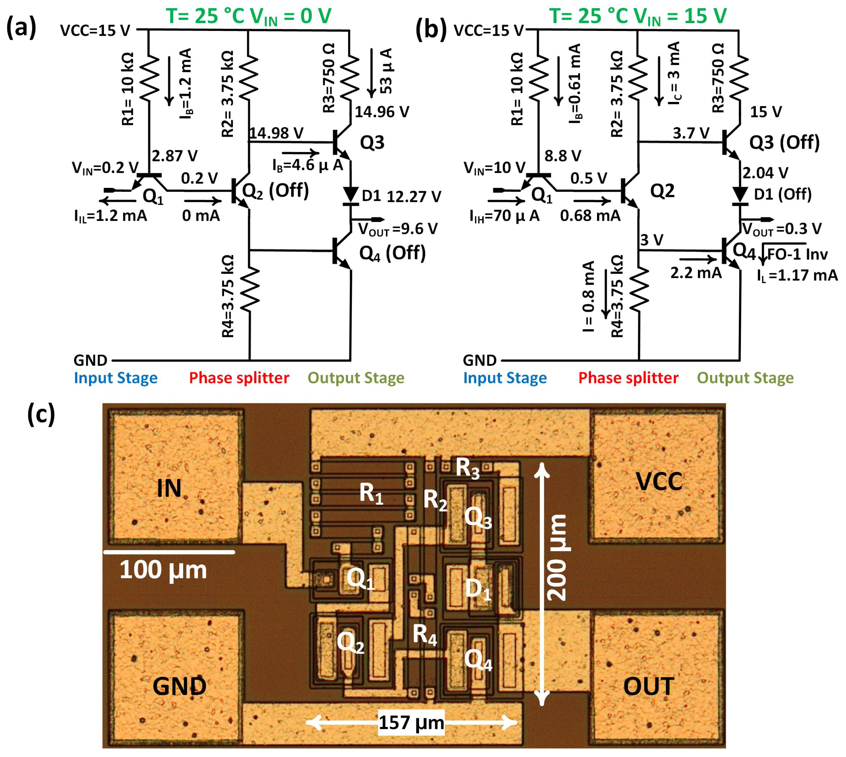
3.1.1. N-P-N Bipolar Transistor

The device from a previous fabrication round that was used to extract models are reported in [21], the simulated forward Gummel plot and forward current gain ( β ) at 25, 300 and 500 °C are shown in Figure 8f,g, respectively, and are used for the circuit design of this work. In order to increase device density per unit area, second generation devices were designed in our group and are used for the circuit fabrication of this work. The second generation devices were characterized at a high-temperature as shown in Figure 8 and their performance analysis for designing TTL-based SiC ICs discussed below.
The output characteristics of the BJT I C vs. V C E as a function of base current at RT, 300 °C and 500 °C are shown in Figure 8a–c respectively. The forward current gain plot ( β vs. I C ) measured at V B C = 0 V at different temperatures is shown in Figure 8e. At room temperature, the current gain ( β ) reaches its maximum value of 103 at I C = 12 mA. At higher I C , the current gain decreases abruptly due to the forward biasing of the base–collector junction at V B E > 8 V [12,13] (see the Gummel plot). The maximum forward current gain is temperature dependent (see Figure 8e). It decreases from 103 at RT to 41 at 300 °C and then increases to 47 at 500 °C. This phenomenon can be attributed to two competing mechanisms at HT: reduction of the emitter injection efficiency due to increased ionization degree of base dopant and the increase of carrier lifetime [12,13].

3.1.2. SiC BJT HT Characteristics Analysis for Designing the TTL-Based Digital Circuits

The current gain β decreases as temperature increases, so the BJT comes out of saturation earlier at higher temperatures (see Figure 8a–c). This observation is important for TTL-based digital circuit fan-out analysis. Around 50% drop in the BJT collector current has been observed by raising the temperature from 25 to 500 °C. The BJT maximum collector current sinking capability while working in the saturation region in the TTL output stage sets the fan-out limit of a TTL gate. Hence TTL gate fan-out decreases around 50% while working at T = 500 °C as compare to working at RT, so SiC bipolar transistors with higher β and I C can increase the TTL circuits fan-out.
The forward Gummel plot ( V B C = 0 V) of the BJT at 25, 300 °C and 500 °C are shown in Figure 8d. The leakage current of the BJT increases at HT because the intrinsic carrier concentration has a positive temperature coefficient. The V B E required to turn ON the BJT, exhibits a temperature coefficient of −2 mV/°C. It can be seen from Figure 8d. and also reported in [21], because of the bandgap-narrowing, that the BJT turns ON around 1 V earlier at temperature = 500 °C as compared to 25 °C. It gives a threshold voltage shift estimate, that SiC based digital circuits required to tolerate and sets the minimum noise margin limit and is discussed in more details in Section 3.2.

3.1.3. Resistors Realized in the Collector Layer

The integrated resistors are realized in the collector layer. A sheet resistance value of 250 Ω /□ at RT was obtained from previous batches and used in the circuit design. This value depends on doping in collector, thickness of collector and over etch in process, so it was expected to change. The standard deviation is 17%, which is due to the non-uniform doping and thickness of the epitaxial layer. The sheet resistance simulated and measured on a die over the wide range of temperature is shown in Figure 9. The temperature dependency is caused by two mechanisms, the degree of dopant ionization and majority carrier mobility. From RT to 200 °C, dopant ionization increases and dominates, so the sheet resistance is reduced. However, from 200 °C to 500 °C majority carrier mobility decreases and dominates so the sheet resistance increases [12,13].
The mean measured value of the sheet resistance is 300 Ω /□ which is around 17% greater than the value used in simulations. The increase in the measured sheet resistance increases the fan-out, the reason is, as it increases the resistance R 1 connected at the base of the input BJT of a TTL gate as shown in Figure 10, by 17% and, hence, reduces the maximum input current when the input will be low. Moreover, the propagation delay is directly proportional to and power dissipation is inversely propositional to the sheet-resistance.

3.2. SiC TTL Digital Gates

Logic circuits including registers, multiplexers, arithmetic logic units (ALUs), and computer memory, all the way up through complete microprocessors, are realized using many gates in a hierarchical design flow. This part demonstrates the design and electrical characterization of in-house-fabricated basic digital gates (Inverters, Buffers, AND, OR, NAND, AND-OR-Invert (AOI)) as building blocks to realize the SiC-based VLSI circuits.

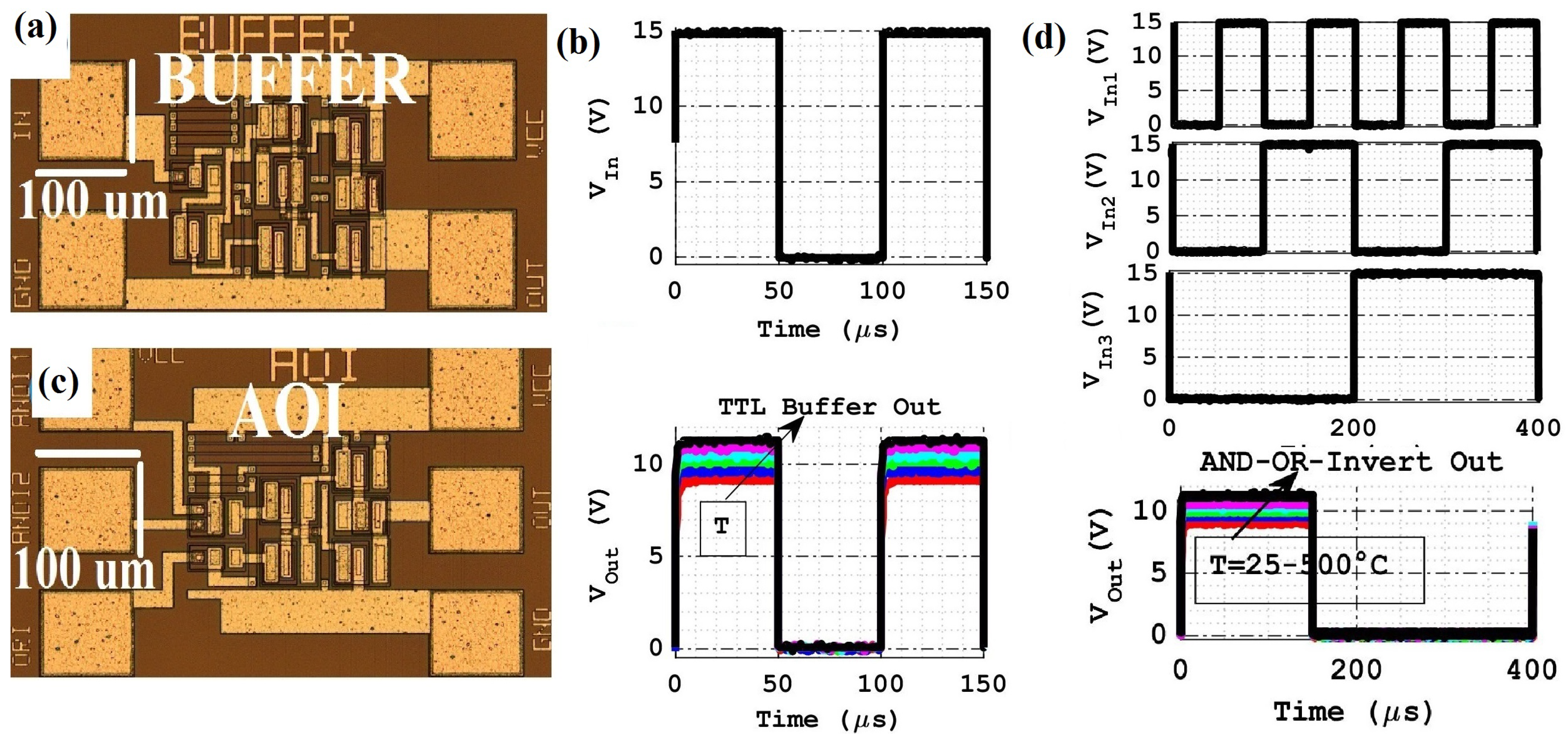
3.2.1. TTL Inverter Design and Characterization

The TTL inverter has been designed, fabricated and characterized over a wide temperature and power supply range as a bench-mark standard cell. The noise margins of the TTL inverter gate were selected as the main design parameter and they are also an important figure of merit for digital circuits. Design of more dense combinational and specially sequential SiC digital circuits is challenging because of the semiconductor device bandgap narrowing and electron mobility variations due to the temperature swing, causes transistor β , I C variation and V B E shift. The V B E required to turn ON the BJT, exhibits a temperature coefficient of −2 mV/°C, hence as compare to 2.2 V at 25 °C required to turn ON the BJT, connected at the input stage (see Figure 10, Q 1 ) of a TTL inverter, it turns ON at 1.2 V at 500 °C (see Figure 8d). In order to tolerate these variations the TTL circuit parameters are modified to provide adequate noise margins and stable voltage levels at HT operations. TTL inverter schematics with simulated node voltages and currents using the HT models [21] at room-temperature in the output-high and low state are shown in Figure 10a,b, respectively, with V C C = 15 V and fan-out of one inverter.
Noise Margin: The voltage-transfer characteristics (VTCs) with power supply of 15 V, with input signal swept between 0 and 15 V, are shown in Figure 11a (both simulated and measured at T = RT to 500 °C). The stable operating points are the highest and lowest intersection points of normal and the inverted VTC curves. The noise margin is the voltage difference between the stable operating point and the knee of the transfer characteristic, defined as the unity slope point.
As shown in the TTL inverter schematic Figure 10a, the TTL inverter input ( V i n ) is 0.2 V, and output ( V o u t ) is 9.6 V. The transistors Q 2 and Q 4 are OFF and Q 3 is ON. Also as shown in the forward Gummel characteristics of the SiC BJT in Figure 8d at RT, when V B E reaches 2.2 V the SiC BJT Q 2 turns ON and phase splitter stage ( R 2 , Q 2 and R 4 ) operates as an amplifier with the gain of − R 2 / R 4 . The V o u t decreases with the negative slope equal to the phase splitter gain and acts as an emitter follower till Q 4 starts conduction. When 2.2 V < V B E Q 2 < 4.4 V the transistors Q 2 and Q 3 will be ON and Q 4 will be OFF, in this range V o u t falls with the gain of around −1 (in order to compensate the process variations, the phase splitter resistance was set as R 2 = R 4 ). When V B E Q 2 drop increases 4.4 V level the the BJT Q 4 turns ON and and reaches saturation before Q 2 and Q 3 turns to cut-off region and V o u t = 0.3 as shown in Figure 10b.
Because of a decrease in the corresponding base-emitter voltage drop, the output-high voltage ( V O H ) increases with the temperature and because of phase splitter gain around −1, the VTC shifts towards the origin, resulting in an increasingly high-level noise margin ( N M H ), while the noise margin-low ( N M L ) decreases with the temperature. As the temperature is increased from 25 to 500 °C, the simulated and measured N M L slightly decreases from 3.7 V down to 1.8 V. The models predict N M L correctly at RT and at 500 °C but at 300 °C the simulated and measured N M L difference is 1 V. This variation can be observed from the VTCs shift with the temperature as shown in Figure 11b. The N M H increases almost linearly from 3.5 to 5.5 V, with the temperature increased from 25 to 300 °C thereafter, it increases up to 7.2 V at 500 °C. The SiC TTL inverter exhibits stable noise margins from RT to 500 °C.
The simulated vs. measured VTCs and noise margins of the inverter as supply-voltage is changed from 8 V to 20 V at three discrete temperatures i.e., T = 25 °C, T = 300 °C, and T = 500 °C, are shown in Figure 12a–c respectively. The output-low voltage ( V O L ) remains fairly constant whereas V O H increases almost linearly with the V C C . Figure 12d shows the noise margins versus the power supply voltage at different temperatures. As the V C C is increased, the N M L only increases by 0.6 V whereas the N M H increases almost linearly with V C C . Figure 12d shows a good match between simulated and measured noise margins.
Fan-out based on simulated results: The fan-out analysis of a TTL gate is important especially for designing complex digital circuits. It gives an estimate of maximum clock driver load and designing clock networks. The silicon based TTL circuits can have a load of 10 gates. Because of the SiC BJT β and I C degradation with the temperature increase and also to accommodate more devices on a unit area the device size was reduced and buffer/repeater circuits have been inserted to address the fan-out.
As shown in Figure 10a the maximum simulated input current is ∼1.2 mA, when the input is low. As reported in [21] maximum current a BJT can sink while working in the saturation so that the output voltage remains low is 19 mA with V O L < 3.8 V at RT (as minimum simulated N M L is 3.8 V at T = 25 °C with V C C = 15 V). The BJT current sinking capability turns down to 9 mA with V O L < 2 V at 500 °C (as minimum simulated N M L is 2 V at T = 500 °C with V C C = 15 V). With these specifications the designed TTL gate can have a fan-out of 16 TTL-gates at RT and it decreases to 7 TTL-gates at 500 °C, which can be verified from the β degradation by increasing the temperature as reported in [21].
Fan-out based on measured results: As discussed previously in the Section 3.1.3 with the 17% increase in the measured sheet resistance, the resistance R 1 with simulated value of 10 kΩ will increase to 11.7 kΩ, hence reduces the maximum input current when the input will be low from 1.2 mA to 1.02 mA with V C C = 15 V. The maximum current a BJT can sink while working in the saturation so that the output voltage remains low is 9 mA at V O L < 3.5 V (as minimum measured N M L is 3.5 V at T = 25 °C with V C C = 15 V), which reduces to 4.4 mA at V O L < 1.8 V (as minimum measured N M L is 1.8 V at T = 500 °C with V C C = 15 V). With these specifications the fabricated TTL gate using the new SiC BJT devices can have a fan-out of 9 TTL-gates at RT and it decreases around 50% to 4 TTL-gates at 500 °C, which is around half of the fan-out of the model devices based calculated fan-out. The new devices based fan-out calculations can be verified from the I C and β degradation by increasing the temperature as shown in Figure 8a–c,e.
Based on the analysis, that the new device collector current sinking capability degradation would be around half of the models device. All the complex TTL-based combinational and sequential circuits, particularly clock tree routing, were designed with the half of the fan-out, that was calculated with the simulated models devices.
Transient-Analysis: The measured performance of a TTL inverter is summarized in Table 2 at 6 discrete temperatures. When the temperature increases from 25 °C up to 500 °C, the output voltage swing increases gradually from 9.4 V up to 11.4 V as the voltage drop V B E decreases with the temperature. Non-monotonic behavior of inverter delays was observed, and all transients are affected by the change in the resistance of the SIC devices.
The propagation delay t P L H is more than three times greater than t P H L , as given in Table 2. The reason is that in the pull-up path there are three resistances as compare to pull-down, which has only one resistance i.e., R C E Q 4 . Moreover, before making a transition from low to high, transistor Q 4 and Q 2 are in saturation. When the input level falls the BJT Q 2 turns first to cutoff-region, whereas Q 4 will continue to operate in the saturation because it needs some time to remove the base charge via resistor R 4 . Because of a race condition; the devices R 3 , Q 3 , and D 1 try to pull-up the output, whereas, Q 4 tries to pull-down until the Q 4 base charge gets removed via R 4 and Q 4 turns off. The propagation delay t P L H can be improved by improving the pull-up devices at the cost of power consumption and area, or by decreasing the R 4 at the cost of noise-margin (the phase splitter sets the slope of the VTC = R 2 / R 4 ).

3.2.2. PDK Gates HT Characterization

NAND, AND, OR Gates: As a proof of concept SiC PDK based designed and fabricated basic digital gates NAND, AND, OR micro-photograph and transient responses are presented in Figure 13. Electrical characterization of a 2-input NAND gate is reported in [18].
Buffer/Repeater: The buffer/repeater circuits are important to address the fan-out/fan-in and to balanced the clock-tree. Micro-photograph of a TTL based buffer/repeater circuit realized in SiC TTL technology is given in Figure 14a and transient response in Figure 14b.
AND-OR-INVERT (AOI): An AOI logic is the fundamental cell used to realize the SR-latches and flip-flops. The Compound logic gates such as AOI are often employed in a circuit design because their construction using TTL is simpler and more efficient than the sum of the individual gates. Micro-photograph and the transient response of an AOI logic circuit designed using conventional TTL configuration are shown in Figure 14c,d, respectively.

3.3. SiC TTL-Based Combinational ICs

3.3.1. Decoder and Multiplexer

A 2–4-line decoder circuit micro-photograph is shown in Figure 15a. and consists of six standard cells (four AND2 gates and two Inverters). This concept can be extended to realize any SiC-based VLSI circuit. The transient response of the decoder is shown in Figure 15b.
A 2–1-line multiplexer micro-photograph implemented using SiC TTL PDK is given in Figure 15c and transient response is shown in Figure 15d; when Sel = 0, MUX passes the V i n 2 at the output, else V i n 1 .

3.3.2. 1-Bit Adder

An ALU of a microcontroller can be realized using basic digital gates and a full-adder. The XOR logic gate and a full-adder circuit are shown in Figure 16. XOR micro-photograph with the transient response is shown in Figure 16a,b respectively, whereas full-adder micro-photograph and transient response is shown in Figure 16c,d, respectively.

3.3.3. Arithmetic and Logic Unit (ALU)

An arithmetic and logic unit is a combinational electronic circuit that performs arithmetic and bitwise logic operations on integer binary numbers. An ALU is a core building block of many types of electronic computing systems, including the central processing unit (CPU) of a computer.
A 2-bit ALU was designed using the SiC TTL PDK. It is a generic building block and can be extended to n-bit arithmetic and logic operations. The ALU performs eight operations (Addition, Pass data on bus B, subtraction using 2’s complement, pass bus B complement, NAND, AND, pass bus A data and OR operation) based on 3-bit opcode (Sel0, Sel1, Sel2). All the operations with 2-bit ALU architecture are shown in the block diagram in Figure 17. The gate level schematic of the ALU was carried out using the PDK gate/module library, manual place and route was done using PDK standard cell library in the Cadence Virtuoso Analog Design Environment. After successful simulation from RT to 500 °C using bipolar HT models [21], DRC and LVS verifications, the circuits were fabricated in the in-house low-power bipolar process. The micro-photograph of the fabricated 2-bit ALU is shown in Figure 18. It consists of 720 integrated devices with a total chip area of 4096 μm × 1765 μm = 7.2 mm2.
The transient response of the ALU, in the range of 25–500 °C with a supply voltage V C C = 15 V, was measured by applying square waves of 10 kHz, 5 kHz, 2.5 kHz and 1.25 kHz with V I H = 15 V, and V I L = 0 V as an input A 0 , B 0 , A 1 , B 1 respectively. The square waves with V I H = 15 V, and V I L = 0 V and frequency of 5 kHz, 2.5 kHz and 1.25 kHz are applied at 3-bit opcode Sel0, Sel1 and Sel2, respectively, to perform the desired selection operation. ALUO0 and ALUO1 are the outputs of the ALU and ALU-CO is the carryout of arithmetic unit that can be used for the ALU integration for an n-bit ALU operations. The measured transient response in the range of 25–500 °C is shown in Figure 19.

3.4. SiC TTL-Based Sequential ICs

3.4.1. Data-type Flip-Flop (DFF)

A Data-type flip-flop (DFF) with asynchronous active high set and reset, was designed using 14 different gates; Inverter, AND, AND-OR-Invert (AOI) and Buffer circuits. AOI logic is the basic cell used to realize the SR-latches and flip-flops [16,24]. The DFF consists of two SR-latches connected in a master–slave configuration.
The micro-photograph of the DFF is given in Figure 20a whereas the transient response of the DFF is shown in (b) and (c), over the temperature range of 25–500 °C, by applying a 10 kHz square wave with V I H = 15 V, and V I L = 0 V as a clock signal. When reset and set inputs are at low logic then at the positive edge of the clock, DFF samples the data input D to the output Q as shown in Figure 20b.
The DFF can also be used as a clock divider by connecting the complementary output QI, to the input D. The transient response of the DFF, configured as a clock divider, in the range of 25–500 °C with a supply voltage V C C = 15 V, was measured by applying square waves of 10 kHz with V I H = 15 V, and V I L = 0 V as a clock input, the DFF output Q is 5 kHz; f c l k divided by 2, as shown in Figure 20c.
The measured performance of TTL-based DFF is summarized in Table 3. When the temperature increases from 25–500 °C, the output voltage swing gradually increases from 9.4 V to 11.4 V, since the corresponding base-emitter voltage drop VBE decrease with the increase in temperature because of the bandgap-narrowing. The transients; setup-time ( t s u p ) and propagation delay of DFF clock-to-Q ( t p c q ) are also temperature dependent. The DFF operates best at 400 °C and consumes minimum energy 145 nJ.

3.4.2. 4-bit Counter

A 4-bit counter was designed using four DFFs with synchronous reset reported in [24], 3 XOR, and 2 AND gates in SiC TTL PDK. The micro-photograph of the fabricated 4-bit counter is shown in Figure 21a. It consists of 520 integrated devices with a total chip area of 3375 μm × 1365 μm = 4.6 mm2. The transient response of the counter, in the range of 25–500 °C with a supply voltage V C C = 15 V, was measured by applying square waves of 10 kHz with V I H = 15 V, and V I L = 0 V as a clock input, when reset turns to low the counter output resets. When reset turns to a logic high then at the positive edge of the clock counter starts counting from 0 to 15 and then again starts from 0 as shown in Figure 21b.

3.5. Analog and Mixed Signal Circuits

Analog and mixed-signal ICs have been successfully designed using the PDK. Analog circuits made in the same bipolar process, but without the PDK, demonstrated up to 500 °C, were reported in [25]. A flash ADC has been implemented using the PDK for HT applications. Encoder and comparator circuits were designed to convert the thermometer code at the output of a comparator to a binary code with the capability of bubble error correction, and successfully integrated with the 4-bit Flash ADC [21]. Moreover, A 10-bit bipolar SAR ADC has been implemented in the SiC bipolar process using the PDK for HT applications [21].

3.6. Reliability

One of the features that need to be explored is the reliability of the SiC based integrated circuits. Reliability testing for the 11-stage ring-oscillator (RO) using SiC TTL PDK indicated that the RO frequency of oscillation decreased 16% after HT characterization [17]. The degradation in DC and transient measurements was permanent, due to the accelerated electro-migration in the Al-based metalization system [26]. The long-term reliability of the SiC ICs at elevated temperatures require stable metalization as reported in [27]. Moreover designing of a microprocessor or more complex VLSI circuits are also limited by the SiC wafer quality.

4. Discussion

The paper has discussed device design and circuit design for HT applications. For the digital circuits realization in this paper we have discussed four main design aspects: delay, power, noise margin, and fan-out. We have concentrated more on the later two aspects, which can be improved with better SiC bipolar devices and circuit design.
Device design for maximum fan-out and noise margins: we have successfully realized complex digital circuits with a fan-out of maximum four gates at T = 500 °C. The fan-out can be improved by increasing the I C sinking capability in the saturation region, by increasing the size of the BJT used to pull down the output. This might increase the chip area but on the other hand smaller number of repeaters will be needed. For the devices demonstrated in the paper, the measured noise margins are enough because β degradation with the temperature increase limits the saturation region. Maximum measured shift was 1.2 V whereas minimum noise margin is 1.8 V. The power dissipation of the TTL gates can be reduced also at the cost of t P L H , by increasing the sheet resistance of the resistors.
TTL circuit design for minimum fan-out and maximum noise margins: The TTL-based digital circuits design can be improved so that we can reduce the buffer/repeaters insertion by restructuring the logic and clock tree networks. Whereas, at the TTL-based gate schematic design level, the fan-out support can be improved by reducing the input current flow when the TTL-gate input is low, by increasing the R 1 connected at the base of the input stage BJT. The noise margins of the TTL gate can be improved by decreasing the gain of the phase splitter, which also improves the propagation delay t P L H , but at the cost of power dissipation.
The SiC TTL-based digital circuits have been realized at two abstraction levels: the PDK design at the device level and digital design at the behavioral, structural or gate level using the PDK. The PDK can be improved by including more devices, design rules, physical verification functionalities, and improving the standard cells if there is a room of improvement for dense integration etc. The digital design flow can be made fully automated that can perform auto place and route ( P & R ) which not only saves time but also chip area.
With the SiC TTL PDK we can design an HT microcontroller with frequency ranges from few hundred kHz to MHz range depending on the data-path, fan-out, noise-margin and operating temperature (non-monotonic temperature dependence). The SiC TTL ICs frequency of operation is according to the demand of HT applications, such as distributed engine control with smart sensors and digital IOs. Employing the SiC ICs the wire count and weight can be reduced, which increases the reliability, expandability and flexibility. Moreover, SiC TTL PDK can also be used for the digital ICs design with sensors and microcontroller for Venus landers applications without active cooling systems and can cut the mission budget significantly. The applications such as space exploration, distributed engine control and sensing, underground drilling etc. can work with low frequency operations for monitoring or controlling purposes and SiC TTL circuits demonstrated here can be designed and employed for specific application requirements.

5. Conclusions

A process design kit has been established for the in-house low-voltage SiC bipolar process. As a proof of concept, SiC-based basic devices and SiC bipolar TTL combinational and sequential ICs have been successfully designed, implemented and fabricated. All the devices, gate/module library and reference ICs have been successfully demonstrated to be operational up to 500 °C. This work has laid the foundation and is an important step towards semi-custom SiC-based application-specific integrated circuits (ASICs) implementation for extreme-environment electronics.

Author Contributions

Conceptualization, C.-M.Z.; methodology, M.S. and C.-M.Z.; validation, M.S., S.H. and R.H.; formal analysis, M.S.; investigation, M.S., and S.H.; writing—original draft preparation, M.S.; writing—review and editing, M.S., S.H., R.H., B.G.M., M.Ö., and C.-M.Z.; supervision, B.G.M., and C.-M.Z.; funding acquisition, B.G.M., M.Ö., and C.-M.Z.

Funding

This research was funded by Knut and Alice Wallenberg Foundation (KAW), project Working on Venus (WoV).

Acknowledgments

The authors would like to thank Panagiotis Chaourani, Dr. Per-Erik Hellström, and Assistant Prof. Saul Rodriguez Duenas for their guidance.

Conflicts of Interest

The authors declare no conflict of interest. The founding sponsors had no role in the design of the study; in the collection, analyses, or interpretation of data; in the writing of the manuscript, or in the decision to publish the results.

References

  1. Cressler, J.D.; Mantooth, H.A. Extreme Environment Electronics; CRC Press: Boca Raton, FL, USA, 2012. [Google Scholar]
  2. National Research Council. Vision and Voyages for Planetary Science in the Decade 2013–2022; The National Academic Press: Washington, DC, USA, 2011. [Google Scholar]
  3. Neudeck, P.G.; Okojie, R.S.; Chen, L.Y. High-temperature electronics—A role for wide bandgap semiconductors? Proc. IEEE 2002, 90, 1065–1076. [Google Scholar] [CrossRef]
  4. Zetterling, C.-M. Integrated Circuits in Silicon Carbide for High-Temperature Applications. MRS Bull. 2015, 40, 431–438. [Google Scholar] [CrossRef]
  5. Young, R.A.R.; Clark, D.T.; Cormack, J.D.; Murphy, A.E.; Smith, D.A.; Thompson, R.F.; Ramsay, E.P.; Finney, S. High Temperature Digital and Analogue Integrated Circuits in Silicon Carbide. Mater. Sci. Forum 2013, 740–472, 1065–1068. [Google Scholar] [CrossRef]
  6. Yu, L.C.; Dunne, G.T.; Matocha, K.S.; Cheung, K.P.; Suehle, J.S.; Sheng, K. Reliability Issues of SiC MOSFETs: A Technology for High-Temperature Environments. IEEE Trans. Device Mater. Reliab. 2010, 10, 418–426. [Google Scholar] [CrossRef]
  7. Ahmad, Shamim. Modeling and Validation of 4H-SiC Low Voltage MOSFETs for Integrated Circuit Design. Ph.D. Thesis, Department of Electrical Engineering, University of Arkansas, Fayetteville, AR, USA, 2015. [Google Scholar]
  8. Francis, A.M.; Rahman, A.; Holmes, J.; Shepherd, P.; Ahmed, S.; Barlow, M.; Bhuyan, S.; Caley, L.; Moudy, T.; Mantooth, H.A.; et al. Design of analog and mixed-signal integrated SiC CMOS circuits with a high fidelity process design kit. In Proceedings of the 39th Annual GOMACTech Conference, Charleston, SC, USA, 31 March–3 April 2014; pp. 555–598. [Google Scholar]
  9. Francis, M.A.; Moudy, T.; Holmes, J.A.; Rahman, A.; Barlow, M.; Ahmed, S.; Mantooth, H.A. Towards standard component parts in silicon carbide CMOS. In Proceedings of the IEEE Aerospace Conference, Big Sky, MT, USA, 7–14 March 2015; pp. 1–9. [Google Scholar] [CrossRef]
  10. Neudeck, P.G.; Spry, D.J.; Chen, L.; Prokop, N.F.; Krasowski, M.J. Demonstration of 4H-SiC Digital Integrated Circuits Above 800 °C. IEEE Electron Device Lett. 2017, 38, 1082–1085. [Google Scholar] [CrossRef]
  11. Hedayati, R.; Lanni, L.; Rodriguez, S.; Malm, B.G.; Rusu, A.; Zetterling, C.M. A Monolithic, 500 °C Operational Amplifier in 4H-SiC Bipolar Technology. IEEE Electron Device Lett. 2014, 35, 693–695. [Google Scholar] [CrossRef] [Green Version]
  12. Lanni, L.; Malm, B.G.; Östling, M.; Zetterling, C.M. 500 °C Bipolar Integrated OR/NOR Gate in 4H-SiC. IEEE Electron Device Lett. 2013, 34, 1091–1093. [Google Scholar] [CrossRef]
  13. Lanni, L.; Ghandi, R.; Malm, B.G.; Zetterling, C.M.; Östling, M. Design and Characterization of High-Temperature ECL-Based Bipolar Integrated Circuits in 4H-SiC. IEEE Trans. Electron Devices 2012, 59, 1076–1083. [Google Scholar] [CrossRef] [Green Version]
  14. Hedayati, R.; Lanni, L.; Shakir, M.; Salemi, A.; Zetterling, C.M. High temperature bipolar master-slave comparator and frequency divider in 4H-SiC technology. In Proceedings of the European Conference on Silicon Carbide Related Materials (ECSCRM), Halkidiki, Greece, 25–29 September 2016; p. 1. [Google Scholar] [CrossRef]
  15. Hussain, M.W.; Elahipanah, H.; Zumbro, J.E.; Schröder, S.; Rodriguez, S.; Malm, B.G.; Mantooth, H.A.; Rusu, A. A 500 °C Active Down-Conversion Mixer in Silicon Carbide Bipolar Technology. IEEE Electron Device Lett. 2018, 39, 855–858. [Google Scholar] [CrossRef] [Green Version]
  16. Ayers, J.E. Digital Integrated Circuits Analysis and Design; CRC Press LLC: Boca Raton, FL, USA, 2004. [Google Scholar]
  17. Shakir, M.; Hou, S.; Malm, B.G.; Östling, M.; Zetterling, C.M. A 600 °C TTL-Based 11-Stage Ring Oscillator in Bipolar Silicon Carbide Technology. IEEE Electron Device Lett. 2018, 39, 1540–1543. [Google Scholar] [CrossRef]
  18. Shakir, M.; Elahipanah, H.; Hedayati, R.; Zetterling, C.M. Electrical Characterization of Integrated 2-Input TTL NAND Gate at Elevated Temperature, Fabricated in Bipolar SiC-Technology. Mater. Sci. Forum 2018, 924, 958–961. [Google Scholar] [CrossRef]
  19. Gummel, H.K.; Poon, H.C. An integral charge control model of bipolar transistors. Bell Syst. Tech. J. 1970, 49, 827–852. [Google Scholar] [CrossRef]
  20. McAndrew, C.; Seitchik, J.; Bowers, D.; Dunn, M.; Foisy, M.; Getreu, I.; McSwain, M.; Moinian, S.; Park, J.; van Wijnen, P.; et al. VBIC95: An improved vertical, IC bipolar transistor model. In Proceedings of the Bipolar/BiCMOS Circuits and Technology Meeting, Minneapolis, MN, USA, 2–3 October 1995; pp. 170–177. [Google Scholar]
  21. Hedayati, R. High-Temperature Analog and Mixed-Signal Integrated Circuits in Bipolar Silicon Carbide Technology. Ph.D. Thesis, KTH Royal Institute of Technology, Stockholm, Sweden, 2017. Available online: http://urn.kb.se/resolve?urn=urn:nbn:se:kth:diva-213697 (accessed on 14 March 2019).
  22. Tian, Y.; Hedayati, R.; Zetterling, C.M. SiC BJT Compact DC Model With Continuous- Temperature Scalability From 300 to 773 K. IEEE Trans. Electron Devices 2017, 64. [Google Scholar] [CrossRef]
  23. Hou, S.; Shakir, M.; Hellström, P.-E.; Zetterling, C.-M.; Östling, M. Process Control and Optimization of 4H-SiC Semiconductor Devices and Circuits. In Proceedings of the Electron Devices Technology and Manufacturing Conference, Singapore, 13–15 March 2019. in press. [Google Scholar]
  24. Shakir, M.; Hou, S.; Zetterling, C.M. A Monolithic 500 °C D-flip flop Realized in Bipolar 4H-SiC TTL Technology. In Proceedings of the European Conference on Silicon Carbide Related Materials (ECSCRM), Birmingham, UK, 2–6 September 2018. in press. [Google Scholar]
  25. Zetterling, C.-M.; Hallen, A.; Hedayati, R.; Kargarrazi, S.; Lanni, L.; Malm, B.G.; Mardani, S.; Norstrom, H.; Rusu, A.; Suvanam, S.S.; et al. Bipolar integrated circuits in SiC for extreme environment operation. Semicond. Sci. Technol. 2017, 32, 034002. [Google Scholar] [CrossRef]
  26. Lanni, L.; Malm, B.G.; Zetterling, C.M.; Östling, M. A 4H-SiC Bipolar Technology for High-Temperature Integrated Circuits. J. Microelectron. Electron. Packag. 2013, 10. [Google Scholar] [CrossRef]
  27. Spry, D.J.; Neudeck, P.G.; Chen, L.; Lukco, D.; Chang, C.W.; Beheim, G.M. Prolonged 500 °C Demonstration of 4H-SiC JFET ICs with Two-Level Interconnect. IEEE Electron Device Lett. 2016, 37, 625–628. [Google Scholar] [CrossRef]
Figure 1. Flowchart summarizing the PDK building process for in-house SiC bipolar low-voltage technology. The feedback provided by the characterization of the devices and circuits to models, simulations, design and fabrication is highlighted by blue arrows (dotted lines), whereas boxes and red arrow indicate steps for the PDK development. The PDK gate schematic is designed using the PDK devices symbols in Cadence Virtuoso Analog Design Environment (ADE). After successful simulations at transistor level using Cadence Spectre simulator, the standard cell physical implementation was carried out in the Cadence Virtuoso ADE. To ensure the correct signal and power routing the design rule check (DRC) layout versus schematic (LVS) programs were created by the Cadence supported physical verification system (PVS) tool. The mask set and process runsheet was used to fabricate the standard cells and devices test structures in the low-voltage SiC bipolar process. The fabricated test structures were measured on wafer. The HT models for the SiC BJTs were created and used for the schematic transistor level simulations.
Electronics 08 00496 g001
Figure 2. The PDK devices P-cells with PDK layers and vias. The multi-emitter bipolar transistors P-cells configured to single-emitter, double-emitter, and triple-emitter are shown on the right hand side respectively. The bipolar transistor circuit diode is made by shortening the base and collector terminals. The epitaxial integrated resistor has its width “W” fixed and the length “L” is parametrized to get the required resistance. The legend for the mask layers and vias are shown on the left hand side.
Electronics 08 00496 g002
Figure 3. Layout implementation of SiC bipolar TTL-based gate using PDK P-cells as a standard cell. For more dense and ease of integration each cell has a standard height, V C C is routed on the top side and G N D on the bottom side of the standard cell. The inputs are on to the left and outputs on to the right side. (Left) An Inverter standard cell illustration using SiC TTL PDK. (Right) 2-input NAND standard cell illustration using SiC TTL PDK.
Electronics 08 00496 g003
Figure 4. The feedback provided by the digital ICs HT characterization, simulations, design and fabrication is highlighted by blue arrows (dotted lines), whereas the right hand side box containing small boxes shows the PDK contents and is used to design the digital circuits. The red arrows and boxes indicate steps of digital ICs realization using SiC TTL PDK. The digital ICs were modeled at behavioral level and structure level using ISE tools such as ModelSim, Matlab, and Quartus II. After that The digital circuits were implemented at transistor level in the Cadence Virtuoso IC design environment using the PDK gate and module library. The transistor level simulations were carried out using the high-temperature compact models. The circuit layout implementation was carried out using the standard cell library. To ensure the in-house standards the physical verification was done using DRC and LVS programs in the Cadence supported PVS tool. The GDSII file was generated to order the masks set. The process runsheet with masks set and SiC wafers were used and circuits were fabricated in our SiC low voltage technology. The fabricated circuits were measured on the wafer. The feedback provided by the characterization of the digital ICs has been used for the functional verification, process optimization and PDK development.
Electronics 08 00496 g004
Figure 5. SiC ICs monolithic integration using SiC PDK. 4 Inverters, 2-input NAND and a Buffer standard cells are integrated as an illustration (a) 5-stage ring-oscillator gate level implementation using PDK gate library (b) 5-stage ring-oscillator place and route using PDK standard cell library.
Electronics 08 00496 g005
Figure 6. Fabricated n-p-n bipolar transistor (a) 2D cross-sectional view, (not to scale) (b) micro-photograph of top view.
Electronics 08 00496 g006
Figure 7. SiC devices and ICs high-temperature measurement setup.
Electronics 08 00496 g007
Figure 8. SiC bipolar transistor output characteristics for designing TTL-based digital circuits. The I C vs. V C E plot of SiC BJT at temperature 25, 300 and 500 °C are shown in (ac) respectively. Around 50% drop in the BJT collector current degradation was measured by raising the temperature from 25 to 500 °C. The forward Gummel plots with ( V B C = 0 V) at 25, 300 and 500 °C are given in (d), the V B E exhibits a temperature coefficient of −2 mV/°C. Forward current gain ( β ) of the BJT measured from RT to 500 °C is shown in (e). Non-monotonic temperature dependence was observed in the BJT I C vs. V C E and β . The simulated forward Gummel plots of the BJTs used for the modeling are shown in (f) with ( V B C = 0 V) at 25, 300 and 500 °C, and Simulated forward current gain ( β ) is shown in (g).
Electronics 08 00496 g008
Figure 9. Simulated and measured sheet resistance over the wide temperature range.
Electronics 08 00496 g009
Figure 10. SiC TTL inverter circuit diagram with node currents, voltages and micro-photograph (a) the output-high state (b) the output-low state (c) micro-photograph.
Electronics 08 00496 g010
Figure 11. SiC TTL inverter (a) simulated vs. measured VTC, (b) noise margins as temperature increases from 25 to 500 °C at V C C = 15 V.
Electronics 08 00496 g011
Figure 12. SiC TTL inverter simulated vs. measured VTC & noise margins as supply-voltage rises from 8 to 20 V at three discrete temperatures i.e., T = 25 °, T = 300 ° and T = 500 °C (a) simulated vs. measured VTC at T = 25 °C (b) simulated vs. measured VTC at T = 300 °C (c) simulated vs. measured VTC at T = 500 °C (d) simulated vs. measured noise margins as the supply-voltage rises from 8 to 20.
Electronics 08 00496 g012
Figure 13. SiC TTL gates micro-photograph with measured transient-response in the range of 25 to 500 °C by applying f i n 1 = 10 kHz f i n 2 = 5 kHz and f i n 3 = 2.5 kHz and f i n 4 = 1.25 kHz, with V I H = 15 V and V I L = 0 V (a) NAND3 micro-photograph (b) NAND3 measured transient-response (c) AND4 micro-photograph (d) AND4 measured transient-response (e) OR4 micro-photograph (f) OR4 measured transient-response.
Electronics 08 00496 g013
Figure 14. SiC TTL Buffer and AOI circuits micro-photograph with measured transient-response in the range of 25 to 500 °C by applying f i n 1 = 10 kHz, f i n 2 = 5 kHz and f i n 3 = 2.5 kHz, with V I H = 15 V and V I L = 0 V (a) TTL Buffer micro-photograph (b) Buffer measured transient-response (c) TTL AOI micro-photograph (d) AOI measured transient-response.
Electronics 08 00496 g014
Figure 15. SiC TTL-based 2–4-line decoder and 2–1-line multiplexer realized in SiC TTL PDK. (a) Decoder micro-photograph (b) measured transient-response in the range of 25–500 °C by applying f i n 1 = 10 kHz f i n 2 = 5 kHz with V I H = 15 V and V I L = 0 V at input. (c) 2–1 Multiplexer micro-photograph (d) MUX measured transient-response in the range of 25–500 °C by applying f i n 1 = 10 kHz f i n 2 = 5 kHz as input and f i n 3 = 10 kHz as a select line with V I H = 15 V and V I L = 0 V.
Electronics 08 00496 g015
Figure 16. SiC TTL-based XOR and full-adder (a) XOR micro-photograph (b) XOR measured transient-response in the range of 25–500 °C by applying f i n 1 = 10 kHz f i n 2 = 5 kHz with V I H = 15 V and V I L = 0 V. (c) Full-adder micro-photograph (d) Full-adder measured transient-response in the range of 25 to 500 °C by applying f i n 1 = 10 kHz at A f i n 2 = 5 kHz at and f i n 3 = 2.5 kHz at Cin with V I H = 15 V and V I L = 0 V.
Electronics 08 00496 g016
Figure 17. 2-Bit ALU block diagram consisting of an arithmetic unit that performs addition and subtraction based on ADD/SUB signal connected to Sel1. The logic unit perform bitwise AND, OR, NAND, and Invert operations. The select lines Sel1, Sel2, and Sel3 are used to select among different logic and arithmetic operations using 2–1 multiplexers. The buffers are used to address the fan-out.
Electronics 08 00496 g017
Figure 18. 2-bit ALU micro-photograph. The white markers on the layout optical image shows the standard cells name, integration density, power and signal routing schemes, in-out ports names and total area. The ALU is comprised of 720 on-chip integrated devices.
Electronics 08 00496 g018
Figure 19. SiC TTL based 2-bit ALU measured transient response over a wide temperature range of 25–500 °C with a supply voltage V C C = 15 V, by applying the square waves of 10 kHz, 5 kHz, 2.5 kHz and 1.25 kHz with V I H = 15 V, and V I L = 0 V as an input A 0 , B 0 , A 1 , B 1 respectively. The square waves with V I H = 15 V, and V I L = 0 V and frequency of 5 kHz, 2.5 kHz and 1.25 kHz are applied at 3-bit opcode S e l 0 , S e l 1   and   S e l 2 respectively to perform the desired selection operation, whereas A L U _ O 0 and A L U _ O 1 are the outputs of the ALU and A L U _ C O is the carryout.
Electronics 08 00496 g019
Figure 20. SiC TTL-based DFF with asynchronous active high set and reset (a) micro-photograph (b) measured transient response in the range of T = 25–500 °C, sampling the data D to Q at a positive edge of the clock ( f c l k = 10 kHz with V I H = 15 V and V I L = 0 V) (c) measured transient response in the range of T = 25 to 500 °C, as a clock divider by connecting the QI to D with f c l k = 10 kHz with V I H = 15 V and V I L = 0 V.
Electronics 08 00496 g020
Figure 21. SiC TTL-based 4-bit counter with synchronous active low reset (a) micro-photograph (b) measured transient response in the range of T = 25–500 °C. The 4-bit counter counts from 0 to 15 at a positive edge of the clock, f c l k = 10 kHz with V I H = 15 V and V I L = 0 V. 4 buffer/repeater circuits are used to address the low fan-out at high-temperature.
Electronics 08 00496 g021
Table 1. List of the TTL gate/module reported in this paper, which are part of the PDK Gate and Module library.
Gate/ModuleNo of InputComb. (C)/Seq. (S)Devices (Transistors + Resistors)
InverterC9
NAND3C9
AND4C11
OR4C20
XOR2C32
Buffer/RepeaterC14
AND-OR-Invert (AOI)C12
2 to 1 MultiplexerC20
2 to 4 DecoderC62
Full-AdderC76
ALUC720
DFF with Set and ResetS120
4-bit CounterS520
Table 2. Measured performance of TTL INVERTER over temperature range of 25 to 500 °C.
Temperature °C V OH / OL [V] t rise / t fall [ns] t PLH / t PHL [ns] T P . P D [nJ]
259.4/0.3990/130450/1257
1009.8/0.3445/90255/604.7
20010.2/0.3380/85235/454.6
30010.8/0.3420/90220/404.5
40011/0.3440/95210/454
50011.4/0.3515/110255/654.7
Table 3. DFF performance summary over wide temperature range.
T [°C] V OH / V OL [V] t r / t f [ns] t sup [ns] t pcq [ns] t P . P D [nJ]
259.4/0.2680/120360720216
1009.8/0.2560/100230520187
20010.2/0.2480/105230400150
30010.6/0.2440/120230400162
40011/0.2520/125240440145
50011.4/0.2540/130250480144

