1. Introduction
Multiplication is an important arithmetic operation widely used in microprocessing and digital signal processing [
1,
2]. Multiplication is realized using a multiplier. This article discusses many quasi-delay-insensitive (QDI) implementations of the array multiplier and contributes by presenting the QDI early output versions of recently reported indicating array multipliers [
3], which leads to simultaneous decreases in cycle time, power-cycle time product (PCTP), and silicon area. The array multiplier has a regular layout and is convenient to pipeline to achieve an increase in the throughput. In fact, the Booth recoded array multiplier is commonly used in floating point multipliers [
4,
5].
Asynchronous multiplier designs have been discussed in the literature [
6,
7,
8,
9,
10,
11]. Some of these are full-custom i.e., transistor-level designs which do not utilize a standard digital cell library and/or the rest utilize the bundled-data handshake protocol for data communication between the current stage and next stage registers of an asynchronous circuit stage by combining single-rail input data with dedicated request and handshake wires. Bundled-data asynchronous multipliers can achieve average-case speed performance which is preferable to the worst-case speed performance of conventional synchronous multipliers. However, bundled-data asynchronous multipliers are not delay-insensitive, and they are susceptible to variations in process, temperature, supply and threshold voltages, and device parameters. This is because the bundled-data handshake protocol is not delay-insensitive and features a fixed delay element whose delay is matched to the maximum delay of the corresponding combinational logic which processes the data. In fact, the delay of the matching delay element is kept slightly greater than the worst-case delay of the combinational logic to accommodate the signal rise and fall times and also the interconnect delay. If the matched delay of the delay element in a bundled-data pipeline stage is exceeded due to any parameter variation, it might result in erroneous data processing and consequently the correct operation of the bundled-data asynchronous circuit cannot be guaranteed.
In the nanoelectronics era, the issue of variability has become prominent due to the relentless shrinkage of transistor dimensions and the associated effects of scaling [
12]. The issue of variability does not bode well for bundled-data asynchronous design. To cope with the issue of variability, the QDI design style is considered to be a robust alternative to the conventional synchronous design [
13]. In this article, we consider many early output QDI designs of the array multiplier and compare them with recently proposed weak-indication array multipliers [
3]. In particular, we propose a novel early output 2-input AND function realization for generating the partial products, which in turn enables a robust, high-speed and low energy realization of QDI array multipliers. Compared to [
3], which presents indicating QDI array multipliers, the proposed early output QDI array multipliers achieve reductions in cycle time and power-cycle time product (PCTP) without increasing the area and without compromising on the robustness.
The rest of the article is organized as follows.
Section 2 gives a background about QDI asynchronous circuit design.
Section 3 discusses the proposed (QDI) early output designs of the array multipliers and distinguishes them from the indicating array multipliers. Henceforth, by ‘early output’ we implicitly mean ‘QDI early output’ unless stated otherwise. Hence, the early output array multipliers are robust like the weak-indication array multipliers.
Section 4 presents the simulation results for the proposed early output and the recently reported indicating array multipliers based on physical realization using a 32/28 nm complementary metal oxide semiconductor (CMOS) process. The simulation results correspond to both return-to-zero (RTZ) and return-to-one (RTO) handshaking. Finally,
Section 5 draws the conclusions.
2. QDI Circuits—Background
QDI circuits are the practically realizable delay-insensitive circuits which incorporate the weakest compromise of isochronic forks [
14]. An isochronic fork assumption implies that all the wire branches arising from a node or junction experience concurrent rising and falling signal transitions. However, for the isochronic fork assumption, a QDI circuit cannot be practically implemented. Generally, the isochronic fork assumption is confined to small circuit areas and thus their physical realization may not be difficult. It was shown in [
15] that isochronic forks are realizable in the nanoelectronics regime, which implies that QDI circuits are feasible in small design geometries.
2.1. QDI Circuit Configuration
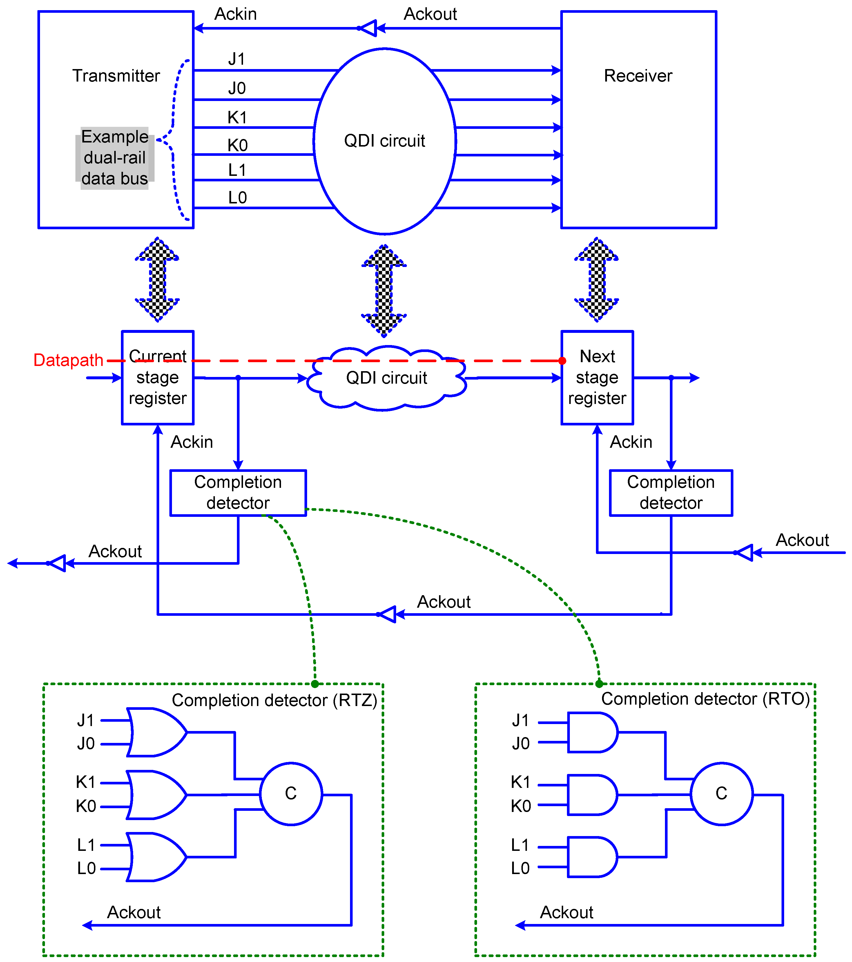
A typical QDI circuit (pipeline) stage is portrayed by
Figure 1, which is correlated with the transmitter–receiver analogy for explanation. In
Figure 1, the current stage and the next stage registers are analogous to the transmitter and the receiver. The QDI circuit is sandwiched between the current stage and the next stage register banks. The register bank comprises a series of registers with one register allotted for each of the rails of a dual-rail encoded primary input. The register is basically a 2-input C-element. An N-input C-element will output 1 or 0 if all the N inputs are 1 or 0, respectively. Even if one input is not identical to the (N-1) inputs of a C-element, the C-element would not change its output but retain its existing steady-state. The circles with the marking ‘C’ represent the 2-input C-elements in the figures.
In
Figure 1, (J1, J0), (K1, K0) and (L1, L0) represent the dual-rail encoded inputs of the single-rail inputs J, K and L respectively. According to dual-rail data encoding [
16] and the 4-phase RTZ handshaking [
17], an input J is encoded as (J1, J0) with J = 1 being represented by J1 = 1 and J0 = 0, and J = 0 is represented by J0 = 1 and J1 = 0. Both these assignments are called ‘data’. The assignment J1 = J0 = 0 is called the ‘spacer’, and the assignment J1 = J0 = 1 is deemed to be illegal since the coding scheme should remain unordered [
18] to maintain the delay-insensitivity.
The application of input data to a QDI circuit that conforms to the 4-phase RTZ handshaking follows this sequence: data-spacer-data-spacer, and so forth. It may be noted that the application of data is followed by the application of the spacer which implies that there is an interim RTZ phase between successive applications of input data. The interim RTZ phase facilitates a robust data communication i.e., handshaking between the transmitter and the receiver. The RTZ handshaking process is governed by the following four steps.
The dual-rail data bus specified by (J1, J0), (K1, K0) and (L1, L0) assumes the spacer, and the acknowledgment input (Ackin) is equal to binary 1. After the transmitter transmits a data, this would result in rising signal transitions (i.e., binary 0 to 1) on one of the dual rails of the entire dual-rail data bus;
The receiver would receive the data sent and drive the acknowledgment output (Ackout) to 1;
The transmitter waits for Ackin to become 0 and after this happens, the dual-rail data bus is reset, i.e., the dual-rail data bus assumes the spacer again;
After an unbounded but a finite and positive time duration, the receiver drives Ackout to 0 and subsequently Ackin would assume 1. With this, a data transaction is said to have been completed and the QDI circuit is allowed to start the next data transaction.
According to dual-rail data encoding and the 4-phase RTO handshaking [
19], an input K is encoded as (K1, K0) with K = 1 being represented by K1 = 0 and K0 = 1, and K = 0 is represented by K0 = 0 and K1 = 1. Both these assignments are called ‘data’. The assignment K1 = K0 = 1 is called the ‘spacer’, and the assignment K1 = K0 = 0 is deemed to be illegal to maintain the delay-insensitivity.
The application of input data to a QDI circuit conforming to the 4-phase RTO handshake protocol follows this sequence: spacer-data-spacer-data, and so forth. It may be noted that there is an interim RTO phase between successive applications of input data. The interim RTO phase facilitates a robust data communication between the transmitter and the receiver. The RTO handshake process is also governed by four steps, which are mentioned below.
Ackin assumes binary 1. After the transmitter transmits the spacer, this would result in rising signal transitions on all the rails of the dual-rail data bus;
The receiver would receive the spacer sent and drive Ackout to 1;
The transmitter waits for Ackin to become 0 and after this happens, it would transmit the data through the dual-rail data bus;
After an unbounded but a finite and positive time duration, the receiver drives Ackout to 0 and subsequently Ackin would assume 1. With this, a data transaction is said to have been completed, and the QDI circuit is allowed to start the next data transaction.
In a QDI circuit, the time taken to process the data (through the datapath highlighted by the red dashed line in
Figure 1) is called ‘forward latency’, and the time taken to process the spacer is called ‘reverse latency’. Because there is an intermediate RTZ or RTO phase between the applications of two input data sequences, the cycle time is expressed as the sum of forward and reverse latencies. The cycle time of a QDI circuit is the equivalent of the clock period of a synchronous digital circuit.
The gate-level details of example completion detectors corresponding to RTZ and RTO handshake protocols are shown in
Figure 1 within the dotted green boxes. A completion detector indicates i.e., acknowledges the receipt of all the primary inputs given to a QDI circuit stage. In the case of RTZ handshaking, Ackout is generated by employing a 2-input OR gate to combine the respective dual rails of each encoded input and then synchronizing the outputs of 2-input OR gates using a C-element or a tree of C-elements. In the case of RTO handshaking, Ackout is generated by employing a 2-input AND gate to combine the respective dual rails of each encoded input and then synchronizing the outputs of 2-input AND gates using a C-element or a tree of C-elements. Ackin is the Boolean complement of Ackout and vice-versa.
2.2. Classes of QDI Circuits
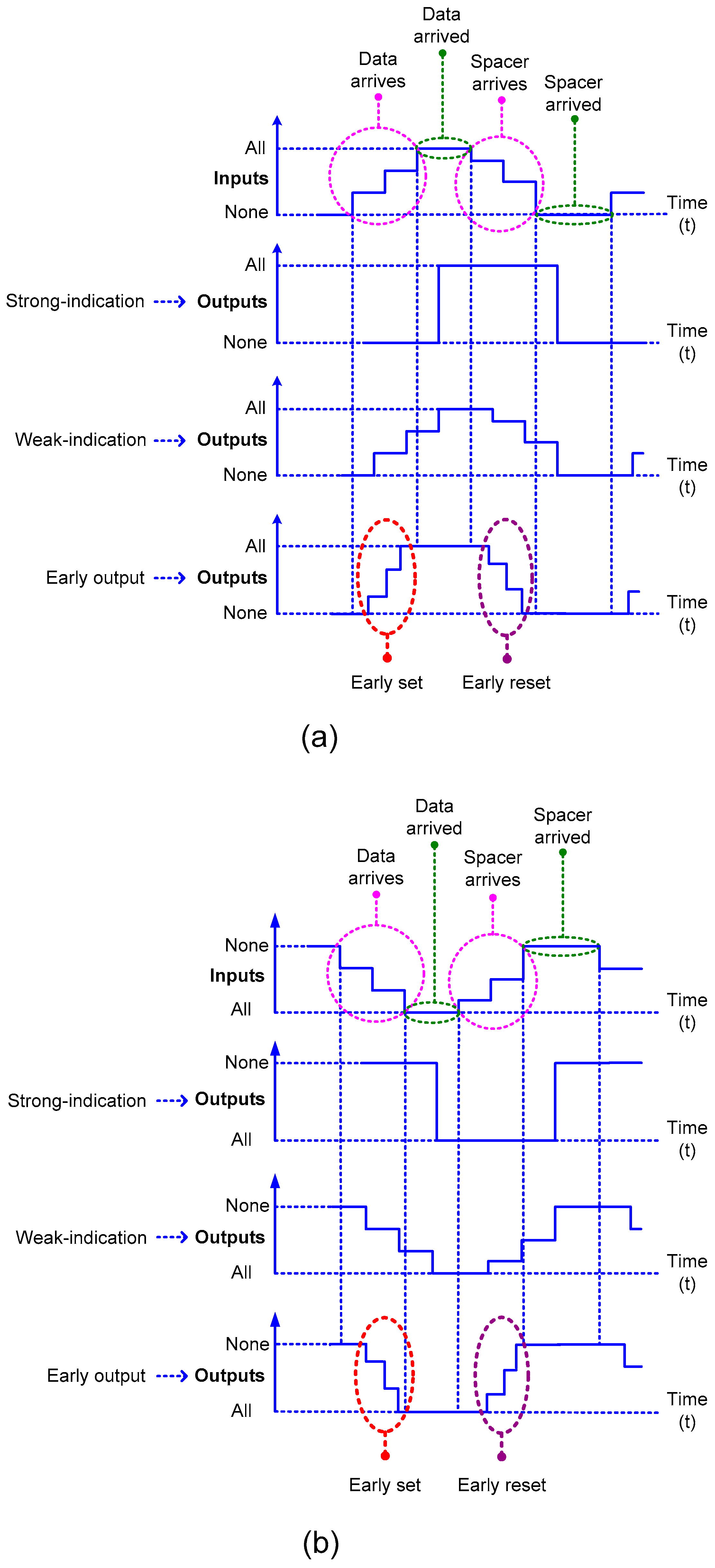
QDI circuits are classified as strong-indication, weak-indication and early output circuits [
20,
21]. The input–output timing correlation of strong-indication, weak-indication and early output circuits are depicted through representative timing diagrams in
Figure 2.
Figure 2a corresponds to RTZ handshaking and
Figure 2b corresponds to RTO handshaking.
Strong-indication circuits would wait to receive all the primary inputs (data or spacer) and after receiving them would process to produce all the primary outputs (data or spacer).
Weak-indication circuits could produce all but one of the primary outputs (data or spacer) after receiving a subset of the primary inputs (data or spacer respectively). However, only after receiving the last primary input would they produce the last primary output.
Early output circuits [
22] are more relaxed in terms of the timing compared to strong-indication and weak-indication circuits. After receiving a subset of the primary inputs (data or spacer), an early output circuit can produce all the primary outputs (data or spacer, respectively), and the late arriving primary inputs would be acknowledged by the completion detector preceding the QDI circuit. If the data is produced early in an early output circuit, it is said to be of early set type, and, if the spacer is produced early in an early output circuit, it is said to be of early reset type. The early set and reset behaviors of an early output circuit are portrayed within the dotted ovals in
Figure 2a,b.
Strong-indication, weak-indication and early output circuits incorporate the isochronic fork(s) assumption. By default, strong-indication and weak-indication circuits are synthesized using safe QDI logic decomposition principles [
23,
24]. Early output circuits, if synthesized by adopting safe QDI logic decomposition principles, are generally QDI.
Safe QDI logic decomposition would ensure that no gate orphans occur in a QDI circuit. By gate orphan, we mean a rising and/or falling signal transition on an intermediate gate output that is not acknowledged by a similar signal transition in the next logic level. Gate orphans are problematic as they could affect the robustness of QDI circuits and they are better avoided by resorting to safe QDI logic decomposition. For an illustration of circuit orphans (i.e., gate orphans and wire orphans) in input–output mode asynchronous circuits, the interested reader is kindly referred to [
21,
25]. Relative-timed circuits [
26] are also early output circuits but they are not QDI because they tend to incorporate extra timing assumptions in addition to the assumption of isochronic forks, which might be sophisticated to realize. In this work, we propose early output array multipliers which are QDI.
QDI circuits are characterized by some generic attributes: (i) a connection of strong-indication sub-circuits could result in a weak-indication circuit, (ii) a connection of weak-indication sub-circuits would result in a weak-indication circuit, (iii) a connection of strong-indication and weak-indication sub-circuits would result in a weak-indication circuit, (iv) a connection of strong-indication or weak-indication sub-circuits and early output sub-circuits could result in an early output circuit, and (v) a connection of early output sub-circuits could result in an early output circuit [
27] or a relative-timed circuit may result [
28].
Among the classes of QDI circuits, an early output circuit is preferable for achieving enhanced optimizations of the design metrics compared to strong-indication and weak-indication circuits. An important reason for this is that early output circuits tend to use more input-incomplete gates contrary to the predominant use of input-complete gates in strong-indication and weak-indication circuits. Input-complete gates are those which require all the inputs to produce the outputs. The well-known input-complete gates are the non-inverting buffer, the inverter (i.e., NOT gate) and the (symmetric) C-element. Input-complete gates are said to be strongly indicating. On the other hand, input-incomplete gates are those which are able to produce the outputs after receiving a subset of the inputs. For example, if one of the inputs to an OR gate is 1, the OR gate could produce the output of 1 regardless of the values of the remaining inputs. It was noted in [
29] that the possible use of input-incomplete gates to replace the input-complete gates would help to better optimize the design metrics of QDI circuits.
3. QDI Array Multipliers
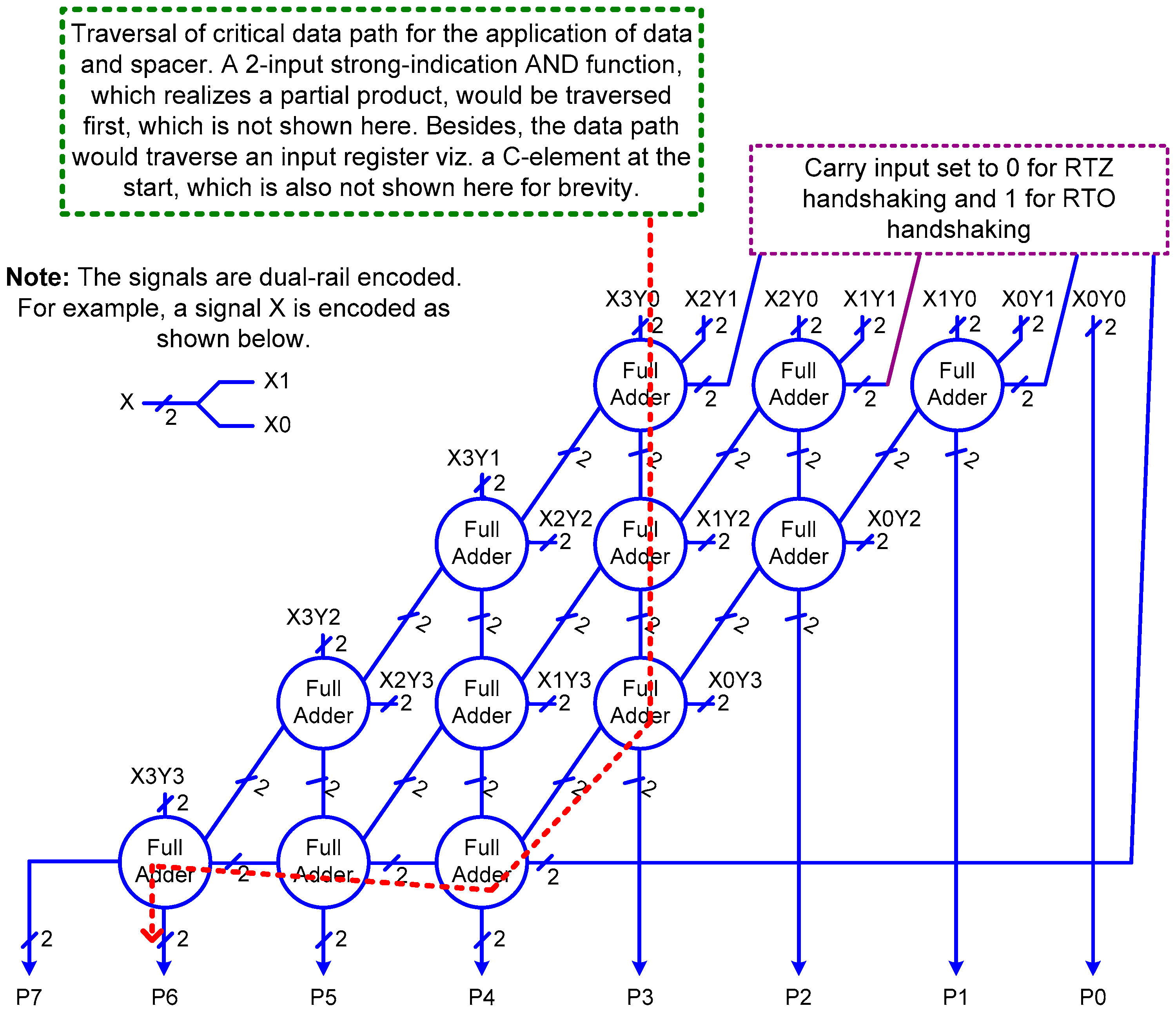
Many QDI array multipliers were implemented based on the 4 × 4 array multiplier structure portrayed by
Figure 3. Here, (X3, X2, X1, X0) and (Y3, Y2, Y1, Y0) represent the single-rail inputs of the multiplier which are dual-rail encoded. (X3, Y3) and (X0, Y0) represent the most significant and the least significant input bit-pairs. P7 to P0 represent the output product bits, with P7 being the most significant product bit and P0 being the least significant product bit. The product bits are also dual-rail encoded. In addition, the partial products and intermediate outputs are dual-rail encoded.
The array multiplier corresponds to the shift-and-add multiplication approach and carry-save addition is performed internally. With respect to
Figure 3, twelve full adders and sixteen 2-input AND functions are used to realize the 4 × 4 array multiplier. Of the twelve full adders, the carry inputs of four full adders are reset, i.e., the carry inputs are set to 0 for RTZ handshaking and they are set to 1 for RTO handshaking. Full adders corresponding to [
30,
31,
32,
33,
34,
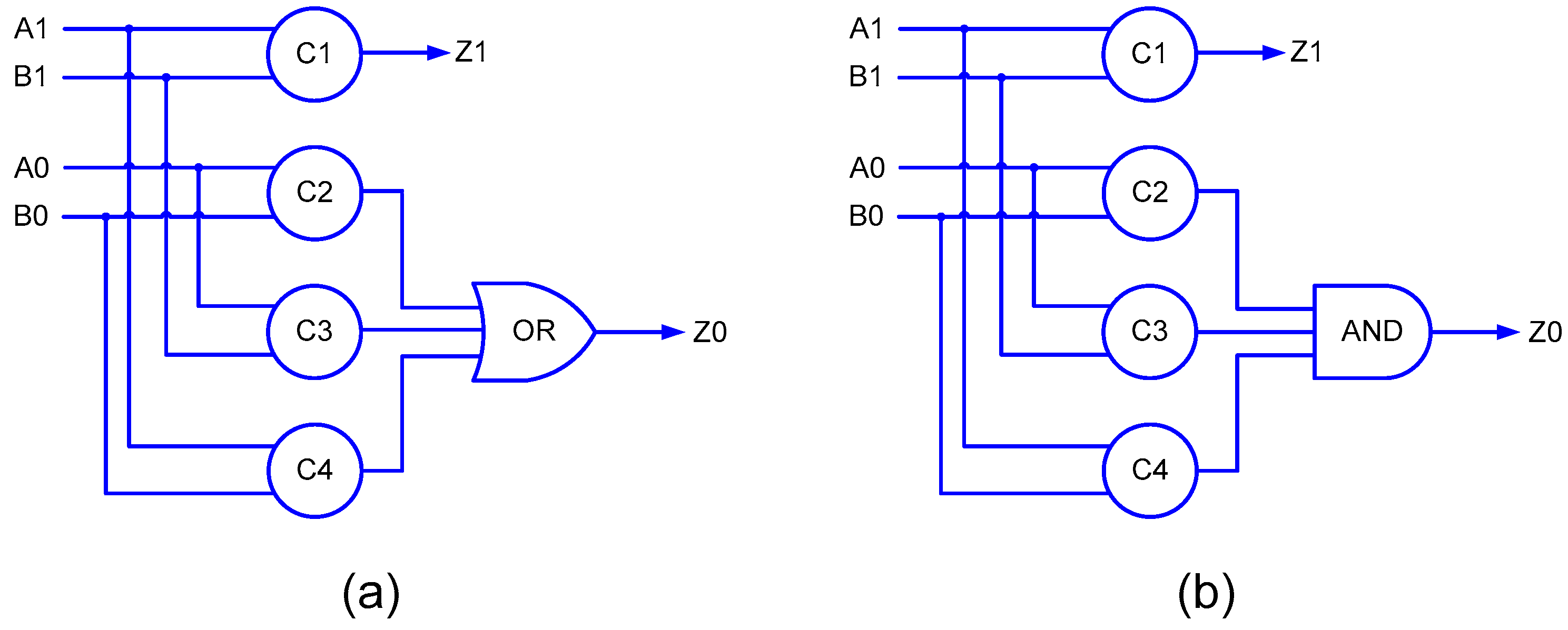
35] have been used to realize the array multipliers. To realize the partial products, a QDI implementation of the 2-input AND function is necessary. In [
3], a strongly indicating implementation of the 2-input AND function, as portrayed by
Figure 4 was used, which corresponds to the delay-insensitive minterm synthesis method [
31].
Figure 4a corresponds to RTZ handshaking and
Figure 4b corresponds to RTO handshaking.
The transformation of an asynchronous circuit that corresponds to RTZ handshaking into one that corresponds to RTO handshaking is subject to certain logic rules, which are discussed along with the proofs in [
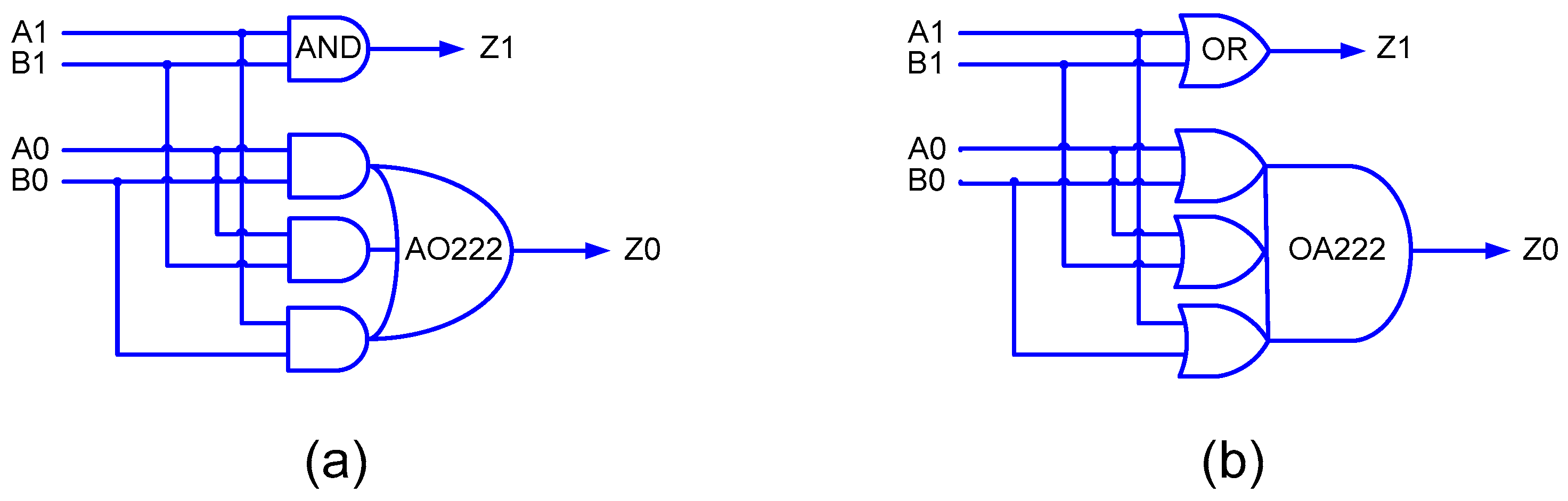
36], and the interested reader is suggested to refer to the same for details. To give a quick idea about the transformation rules, if the gates in an asynchronous circuit which correspond to RTZ/RTO handshaking are replaced by their respective duals, an equivalent asynchronous circuit that corresponds to RTO/RTZ handshaking will result. Nevertheless, it is important to note that C-elements are an exception in this regard and they are retained as such along with their respective inputs. In this work, we propose a new early output implementation of the 2-input AND function, as shown in
Figure 5.
Figure 5a corresponds to RTZ handshaking and
Figure 5b corresponds to RTO handshaking. In
Figure 4 and
Figure 5, (A1, A0) and (B1, B0) represent the dual-rail encoded inputs of the 2-input AND function, and (Z1, Z0) represents the dual-rail encoded primary output.
In
Figure 4, C1, C2, C3 and C4 represent 2-input C-elements. The 2-input C-element was custom-realized by modifying the AO222 gate by introducing feedback as in [
37], which required 12 transistors. Four 2-input C-elements and a 3-input OR/AND gate were used to realize the strong-indication 2-input AND function, which required a total of 56 transistors for a static CMOS implementation. On the other hand, in
Figure 5, one 2-input AND/OR gate and an AO222/OA222 complex gate is used to realize the early output 2-input AND function, requiring a total of only 18 transistors. Hence, the proposed early output 2-input AND function, which is used for generating the partial products, requires 68% fewer transistors than the strongly indicating 2-input AND function. In terms of area, the former requires 57% less silicon than the latter with respect to RTZ handshaking and 56% less silicon than the latter with respect to RTO handshaking based on implementation using a 32/28 nm CMOS technology [
38]. From the critical path delay perspective, based on theoretical calculations involving the typical propagation delays of gates, the early output 2-input AND function exhibits 41 and 48% less delay than the strong-indication 2-input AND function with respect to RTZ handshaking and RTO handshaking, respectively. These observations suggest that the use of the (proposed) early output 2-input AND function could pave the way for reductions in area (and power and energy) and cycle time of the QDI array multiplier.
Besides the reductions in design metrics that are achievable using the early output 2-input AND function, there is another observation to note. In [
3], weak-indication array multipliers were realized using strong-indication/weak-indication full adders of [
30,
31,
32,
33,
34,
35] and the strong-indication 2-input AND function as shown in
Figure 4. Here, because the early output 2-input AND function is used to generate the partial products, the resulting QDI array multipliers are said to correspond to the early output type. To explain this briefly, let us refer to
Figure 5a. Supposing A1 and B1 are set to 1 during a data phase, Z1 will assume 1. In the subsequent RTZ phase, even if A1 assumes 0 before B1, Z1 will become 0. The late reset of B1 (to 0), which may not be acknowledged by the array multiplier, will nevertheless be acknowledged by the completion detector preceding the array multiplier. This is because the isochronic fork assumption is imposed on all the primary inputs and thus no wire orphan would occur. A wire orphan refers to an unacknowledged signal transition on a wire which is eliminated by incorporating the isochronic fork assumption [
21].
It may be noticed from
Figure 3 that the partial products are processed in the array multiplier by a carry-save adder (CSA) which is comprised of strong-indication or weak-indication full adders. The receipt of all the partial products would be acknowledged by the sum outputs of the full adders although the carry outputs of the full adders may or may not fully acknowledge, especially when a weak-indication full adder is used. In addition, the intermediate sum and carry outputs produced by the full adders at a particular logic level would be acknowledged by the sum outputs of the full adders present in the next logic level and hence there does not arise a possibility for the occurrence of gate orphan(s).
4. Implementation Results and Discussion
In total, twenty-eight 4 × 4 QDI array multipliers corresponding to weak-indication and early output timing models were implemented, with fourteen corresponding to RTZ handshaking and the same fourteen corresponding to RTO handshaking using a 32/28 nm CMOS technology [
38].
To conveniently refer to the array multipliers, we use certain legends as given in the second column of
Table 1. In the legends, ‘M’ refers to the multiplier. The prefix ‘Z’ before M1 to M7 implies that the array multipliers correspond to RTZ handshaking, and the prefix ‘O’ before M1 to M7 implies that the array multipliers correspond to RTO handshaking. ‘WI’ refers to weak-indication and ‘EO’ refers to early output in
Table 1—these are mentioned within brackets in the second column.
A typical case process-voltage-temperature (PVT) specification corresponding to a high V
t bulk CMOS process with a supply voltage of 1.05 V and an operating temperature of 25 °C was considered to perform the simulations. About 2000 random input vectors, half of which represents data and the remaining representing the spacer, were supplied to the array multipliers assuming a cycle time of 8 ns with a 50% duty cycle to simulate the multiplier function. A logical equivalence was maintained between the input vectors corresponding to 4-phase RTZ and RTO handshaking. Based on the functional simulations, the switching activity data were captured which were subsequently used to estimate the average (total) power dissipation. Synopsys tools were used to estimate the design metrics viz. cycle time, area, and average (total) power dissipation, and these are given in
Table 1. As mentioned in the previous section, the QDI array multiplier is realized using QDI full adders and 2-input AND functions. Hence, references to the corresponding literature with respect to the full adders used which pertain to different asynchronous logic design methods, are mentioned in the third column of
Table 1. To realize the (weakly) indicating array multipliers corresponding to RTZ and RTO handshaking, the strong-indication 2-input AND function realizations shown in
Figure 4a,b were used. On the other hand, to realize the early output array multipliers corresponding to RTZ and RTO handshaking, the proposed early output 2-input AND function realizations shown in
Figure 5a,b were used.
The cycle time is given by the sum of forward and reverse latencies. The forward latency of a QDI circuit is like the critical path delay of a synchronous circuit which can be directly estimated through static timing analysis. However, estimating the reverse latency of QDI circuits is rather non-trivial since it reflects the time taken to process the spacer. The reverse latency can, however, be estimated based on the timing information corresponding to the gate-level simulations. For the QDI array multipliers mentioned in
Table 1, their forward and reverse latencies are equal since indicating full adders are used, and the critical datapath traversed within the array multiplier to process the data or the spacer is the same, which is highlighted by the red dashed line in
Figure 3.
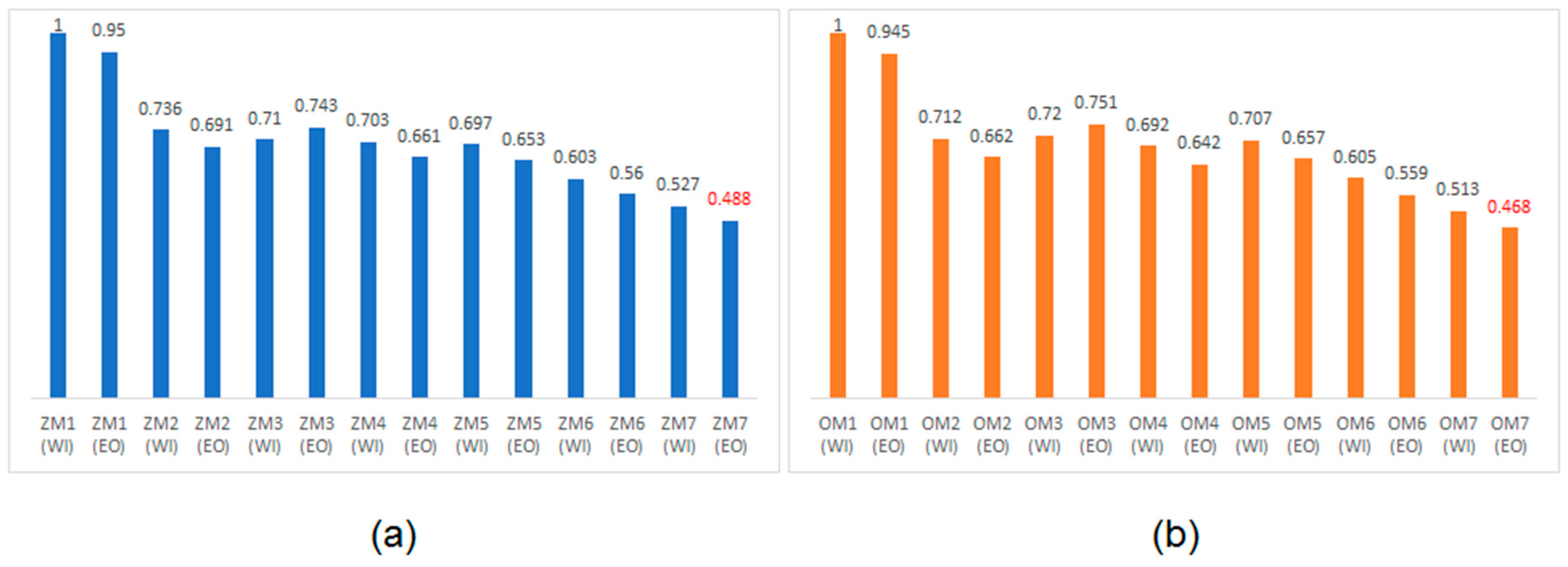
Since power dissipation and cycle time are desirable to be less, PCTP is also desired to be less. The PCTP serves as a qualitative low energy parameter for a QDI circuit and is analogous to the power-delay product of a synchronous circuit. The PCTPs of QDI array multipliers were manually calculated using the power and cycle time values given in
Table 1. To normalize the PCTPs, the highest value among the calculated PCTP values corresponding to a particular handshake protocol was considered as the reference, and this value was used to divide the PCTPs of all the array multipliers corresponding to that handshake protocol. This procedure was followed to normalize the PCTPs of the array multipliers corresponding to RTZ and RTO handshaking, separately. Hence, the minimum value of PCTP is representative of the best QDI array multiplier with respect to RTZ or RTO handshaking. The normalized PCTPs of the QDI array multipliers corresponding to RTZ and RTO handshaking are plotted in
Figure 6a,b, respectively, and the data labels are also shown. In
Figure 6a,b, the red data labels specify the optimum PCTPs.
It is seen from
Table 1 that the average power dissipation of the QDI array multipliers does not vary significantly. This is because all the QDI array multipliers incorporate the monotonic cover constraint (MCC) [
17] in their logic realization. The MCC signifies the activation of one signal path from a primary input to a primary output after the supply of input data. The MCC, when satisfied, ensures the proper indication of rising or falling signal transitions throughout an entire QDI circuit over the entire circuit depth. Generally, in QDI circuits, the signal transitions, whether they are rising or falling, should occur monotonically throughout the entire circuit [
39] from the first logic level up to the last logic level to ensure unambiguous indication. This would be guaranteed if the MCC is incorporated into the logic description and a safe QDI logic decomposition is performed.
The MCC is satisfied by adopting a logic format which is composed of disjoint terms [
40] governing the primary outputs. For example, in a disjoint sum-of-products expression, the logical conjunction of any two products would yield 0 since the product terms are mutually orthogonal. Hence, only one term would be activated in a disjoint logic expression for the application of input data.
A couple of general inferences can be derived from
Table 1: (i) the proposed early output array multipliers achieve considerable reductions in cycle time, area and power dissipation (and also PCTP) compared to the indicating array multipliers [
3], and (ii) the RTO handshaking enables a consistent reduction in all the design metrics (and also PCTP) compared to the RTZ handshaking for the QDI array multipliers.
Referring to
Table 1, it is found that, overall, the proposed early output array multipliers when compared with the indicating array multipliers enable average reductions in cycle time, area, power dissipation and PCTP by 3.4%, 17.7%, 1.3% and 4.7%, respectively, with respect to RTZ handshaking, and average reductions in cycle time, area, power dissipation and PCTP by 4.2%, 17.9%, 1.2% and 5.3%, respectively, with respect to RTO handshaking. Considering only the early output array multipliers, the RTO handshaking enables a 3.7% reduction in cycle time and a 4.1% reduction in PCTP compared to the RTZ handshaking, on average, with no increase in the area.
Referring to
Figure 6, among the various QDI array multipliers, it is noted that ZM7 (EO) and OM7 (EO) report the least PCTP with respect to RTZ and RTO handshaking, respectively. Among the various QDI array multipliers in
Table 1, the proposed early output array multiplier corresponding to RTO handshaking i.e., OM7 (EO) reports the least cycle time and the optimum PCTP compared to the rest. In comparison with its RTZ handshake counterpart, i.e., ZM7 (EO), OM7 (EO) reports a 6.6% reduction in cycle time and a 6.7% reduction in PCTP with no increase in the area.


