Article

A Semi-Floating Gate Memory with Tensile Stress for Enhanced Performance

School of Microelectronics, Fudan University, Shanghai 200433, China
*
Authors to whom correspondence should be addressed.
Electronics 2019, 8(4), 414; https://doi.org/10.3390/electronics8040414
Submission received: 18 March 2019 / Revised: 1 April 2019 / Accepted: 2 April 2019 / Published: 9 April 2019
(This article belongs to the Section Microelectronics)

Abstract

:
With the continuous scaling down of devices, traditional one-transistor one-capacitor dynamic random access memory (1T-1C DRAM) has encountered great challenges originated from the large-volume capacitor and high leakage current. A semi-floating gate transistor has been proposed as a capacitor-less memory with ultrafast speed and silicon-compatible technology. In this work, a U-shaped semi-floating gate memory with strain technology has been demonstrated through TCAD simulation. Ultra-high operation speed on a timescale of 5 ns at low operation voltages (≤ 2.0 V) has been obtained. And the tensile stress induced in its channel region by using contact etch stop layer (Si3N4 capper layer) was found to significantly improve the drain current by 12.07%. Furthermore, this device demonstrated a favorable retention performance with a retention time over 1 s, and its immunity to disturbance from bit-line has also been investigated that could maintain data under the continuous worst writing disturbance operation over 10 ms.

1. Introduction

The large volume capacitor of the one transistor (1T)-one capacitor (1C) DRAM has limited its further applications in advanced memory fields with shrinking cell size [1,2,3]. Various capacitor-less memory devices have thus been proposed to avoid the problems associated with the scaling of a capacitor and achieve high memory density [4,5,6,7,8]. One promising candidate is the semi-floating gate transistor (SFGT) with an embedded tunneling field-effect transistor (TFET) [8,9]. The structure of a semi-floating gate to restore charges and the embedded TFET for charging has enabled a high writing speed with low operation voltage. However, the drain current of the SFGT is relatively small leading to unsatisfactory sensing capabilities due to the tunneling mechanism which is similar to that of traditional TFET devices.
The employment of strain technologies in modern electronic devices to improve mobility and drive current has been developed for decades in advanced complementary metal-oxide-semiconductor (CMOS) transistors [10,11,12,13,14,15]. However, most of these technologies, such as embedded SiGe [10] and embedded Si:C [13], request complex process steps, making them not suitable or transferrable to a wider range of advanced processes. Hence, the tensile-stress contact etch stop layer (CESL) has gained popularity for its simplicity as well as good reliability and has been integrated into the CMOS fabrication process [14,15,16,17,18,19].
Here, we performed a 2D simulation study on a U-shaped channel SFGT memory by using Sentaurus TCAD [20] tool based on the 40 nm technology node. The mechanical stress introduced by tensile Si3N4 capper layer was found to be effective in enhancing the drain current by 12.07%. In addition, the retention and disturbance performance of the U-shaped SFGT memory were systematically studied as well.

2. Simulation and Results

2.1. Device Structure and Operation

The structure and doping contour of the U-shaped SFGT memory with the Si3N4 capper layer are shown in Figure 1a. The channel of the U-shaped floating-gate metal-oxide-semiconductor field-effect transistor (FG-MOSFET) is recessed into the substrate to increase the physical channel length of the MOSFET, which is expected to alleviate the short channel effect and obtain larger Cox to store more charges. A PN junction is formed via a contact window between the p+ doped U-shaped semi-floating gate (SFG) and the n+ doped drain region. The control gate (CG) extended over the PN diode makes it an embedded TFET, which can regulate charges in the SFG. Moreover, to introduce mechanical stress in the channel of the FG-MOSFET, a 100 nm Si3N4 capper layer with intrinsic stress of 1 GPa is deposited over the device.
The simulated transfer characteristic of the U-shaped SFGT memory is presented in Figure 1b. The VD is set to 1.0 V, and the VCG is swept from −2 V to 2 V in dual sweep model. The embedded TFET is turned on at the initial time with VCG of −2 V and positive charges are written into the SFG. Meanwhile, the increase of VCG also contributes to a higher SFG potential to turn on the FG-MOSFET. And the TFET is nearly switched off when the VCG becomes positive. However, the high potential of the SFG still keeps the FG-MOSFET at on state and the drain current almost keeps unchanged. With increasing VCG, the PN junction of the embedded TFET becomes forwardly biased and the charges in the SFG are emptied resulting in a high threshold voltage (Vth). Then, the FG-MOSFET is turned off with a decreasing VCG during back sweeping. As shown in Figure 1b, the threshold voltage has shifted ~3.0 V between state 0 and state 1 by modulating the amount of charges in the SFG through the embedded TFET.
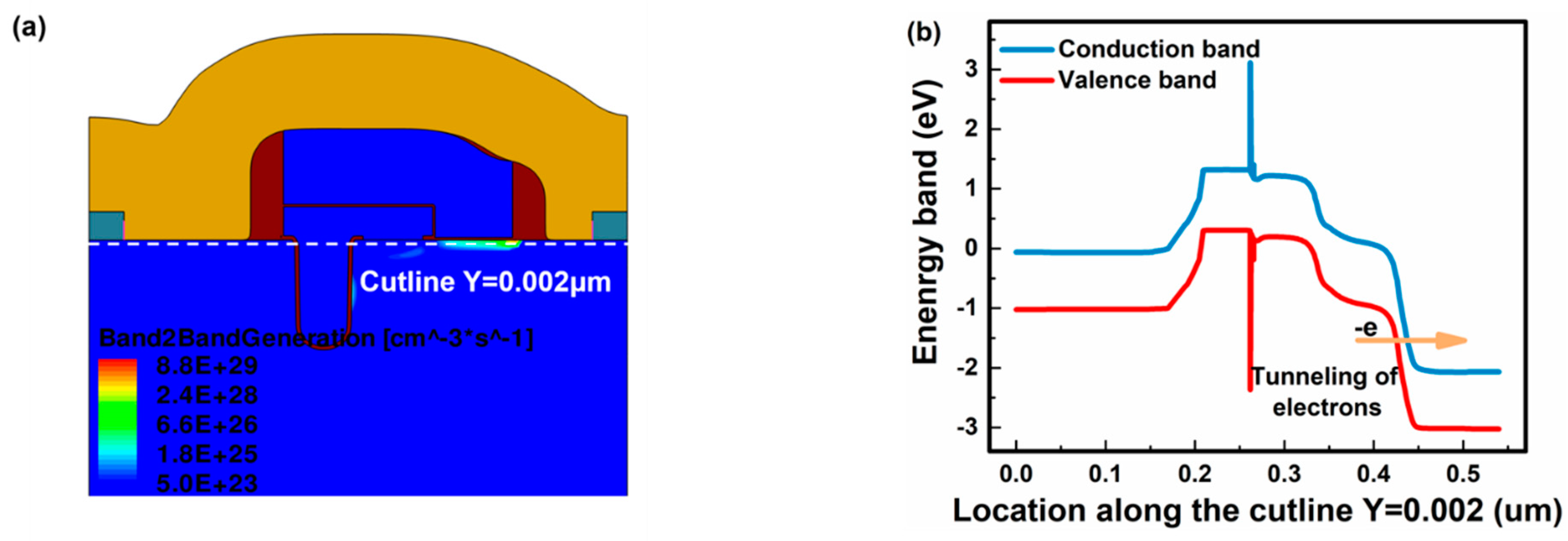
The operation condition of the U-shaped SFGT memory is illustrated in Table 1. During the write-1 operation, the positive bias of 1.4 V for VD lowers the energy band of the drain region while the control gate with a negative bias of −2.0 V inverts the n-doped drain extension region that boosts the energy band. Therefore, band-to-band tunneling (BTBT) occurs at the place where the energy band bends the strongest. The rate contour of the BTBT generation is shown in Figure 2a. The Kane BTBT model [21,22] is used to calculate the band-to-band generation rate, which is expressed as follows:
G BTBT = A BTBT × E 2 E g 1 2 × exp ( B BTBT × E g 3 2 E )
where ABTBT and BBTBT are constants, E is the magnitude of the electric field, and Eg is the band-gap energy. Figure 2b has exhibited the corresponding energy band diagram along the horizontal cutline Y = 0.002 μm below extended control gate. Electrons from the valence band of the n− channel under the extended CG tunnel across the band gap to the conduction band of the n+ drain region, so that current flows from the drain region to the SFG. Then, the increased positive charges which are stored in the SFG cause a lower Vth.
During the write-0 operation with 0.6 V VD and 1.5 V VCG, the electrostatic potential of the SFG is higher than that of the drain region. Therefore, the PN junction of the embedded TFET is forwardly biased and the current flows from the SFG to the drain region. And positive charges in the SFG that are emptied have resulted in a higher value of Vth. Additionally, reading is operated when the embedded TEFT is turned off with 1.4 V VD and 0.7 V VCG. The reading operation is nondestructive because the PN junction of the embedded TFET is reversely biased and the charges in the SFG are retained. The different read-out current between state 1 and state 0 is due to the different Vth of the FG-MOSFET, which depends on charges in the SFG because of capacitive coupling.
By optimizing the writing voltage VCG and writing time of the write-1 operation, the U-shaped SFGT memory can obtain a sufficient sensing window for state 1 and state 0 as well as a high writing speed at low operation voltages. Figure 3a shows the dependence of electrostatic potential change (ΔEP) of the SFG on VCG during write-1 operation. With a writing time of 5 s and the VD of 1.4 V, a lower negative VCG bends the energy band more significantly, resulting in more positive carriers written into the SFG. But when VCG at −2.4 V and −2.8 V, the ΔEP changes a little since excessive charges were written into the SFG that would diffuse out for its concentration gradient distribution. Hence it is better to choose the VCG of −2.0V for write-1 operation. Figure 3b shows the relation between ΔEP of the SFG and the writing time for write-1 operation while keeping VCG at −2.0 V and VD at 1.4 V. Since the BTBT takes place during the entire writing time, a close-to-linear relationship has been observed between ΔEP and writing time. Therefore, to achieve an ultra-high writing speed and an adequate sensing window (~6.8 μA/μm in Figure 4b) at a relatively low operation voltage, −2.0 V and 5 ns are selected as the optimal values for control gate voltage VCG and writing time of the write-1 operation, respectively.

2.2. Effect of the Tensile-Stress CESL

The poly gate of the U-shaped SFGT is stretched laterally as the tensile Si3N4 capper layer are deposited on top of the device. Accordingly, tensive strain is introduced in the U-shaped channel region along the channel direction. In Sentaurus Process simulation, the stress-rebalancing step is conducted to re-establish the stress equilibrium in the structure to calculate the process induced mechanical stress. The effects of stress can be illustrated by employing the deformation potential model, strained effective mass and density of states (DOS) model for strained band gap as well as stress dependent mobility model in Sentaurus Device simulator [20,21]. As shown in Figure 4a of the lateral strain Stress XX distribution, there is compressive strain in the source and drain region while tensive strain exists in the channel region along the channel direction. The average value of lateral Stress XX under the U-shaped channel is 28 MPa. Benefited from the tensive strain, electrons transfer into the lower-energy level conduction band with lower conductivity mass, and the intervalley scattering is also suppressed [11]. Both effects have contributed to a higher electron mobility., which further induces a higher drain current in the device.
Figure 4b shows the simulation results demonstrating the drain current improvement of the U-shaped SFGT by the tensive Si3N4 capper layer. The voltages of the operation sequence are applied according to Table 1. It is found that the read-out current of state 1 for the U-shaped SFGT memory with Si3N4 cap layer has reached up to 6.87 μA/μm which shows a 12.07% increase as compared with that in the conventional structure without the Si3N4 cap layer. Furthermore, the read-out current ratio of state 1 and state 0 is as high as 4.5 × 10⁴ for the U-shaped SFGT memory with the Si3N4 cap layer.

2.3. Retention and Disturbance Performance

The retention performance of SFGT memory has also been systematically explored. As shown in Figure 5a, the retention time of state 0 and state 1 is both over 1 s which means that it is unnecessary to refresh the memory frequently. The simulation is executed as VCG and VD are kept at the standby condition after data ”1” or data “0” has been written. For state 1, the amount of positive charges in the SFG is not sufficient enough to make the SFG potential higher than that in the drain region when the device is operated by VCG ~0 V and VD ~1.0 V. As a result, the PN junction between the SFG and the drain region is reversely biased. But at the same time, positive charges diffuse outside the SFG because of the concentration gradient, leading the degradation in the read-out current of state 1 after a long retention time. On the other side, the PN junction is also reversely biased for the retention situation of state 0 for the higher potential of drain region than the SFG. Thus, the reverse leakage current from the drain region to the SFG makes state 0 approaching state 1 over a long retention time of 1 s. The longer retention time can reduce the power consumption for frequent refresh operation of memory.
Considering the U-shaped SFGT memory array programmed by page, cells connected to columns in the same row are simultaneously operated. Thus, each cell may be subjected to disturbances from the bit-line (VD). The memory cell was first written to data 1 or data 0 and then kept in the hold state with the VCG of 0 V and VD of 1.0 V. When the neighboring cells from different rows but the same column were operated by write-0, write-1, or reading, disturbances occurred that VD was kept in disturbance conditions because of a shared bit-line. The disturbance performance shown in Figure 5b was obtained by simulating a certain disturbance time.
There are six types of disturbances in total on state 1 and state 0 from the bit-line, but they can be simplified to four types for the same VD of write-1 and reading operation. For state 1, the most serious disturbance is the VD-write-0 disturbance with VD of 0.6 V and VCG of 0 V when the PN junction is weakly reversely biased for the relatively higher potential of the SFG with more positive charges. However, state 1 is still weakened after 100 ms of disturbance time since there are diffusion currents flowing from the SFG to the drain region. The other type of disturbance on state 1, that is, the VD-write-1 disturbance with VD ~1.4 V and VCG ~0 V does not degrade state 1. This is because more charges are written into the SFG as the embedded TFET is lightly turned on. Then, the read-out current increases slowly over a long period of time. As for the disturbance on state 0, the PN junction is reversely biased due to the low SFG potential of state 0 during the VD-write-0 disturbance. Hence, the read-out current almost keeps unchanged. When it is disturbed by the VD-write-1 operation, the embedded TFET is also weakly turned on such that charges are written into the SFG slowly. Thus, the read-out current of state 0 increases as the disturbance continues. As shown in Figure 4b, the state of the memory could still be distinguished when suffering from the worst disturbance over 10 ms, which means the SFGT memory is immune to at least 2 × 10⁶ times of the continuous writing disturbance operations.

3. Conclusions

A novel U-shaped SFGT capacitor-less memory utilizing the CESL strain technology has been investigated in this work. It could be programmed with a low operating voltage (≤ 2.0 V) and a short operation time (~5 ns). And the tensive strain in the U-shaped channel region which was introduced by the strained Si3N4 capper layer has improved the read-out current by 12.07%. More importantly, the SFGT memory cell obtained a retention time over 1 s that decreases the refresh rate and dynamic power consumption than the traditional 1T-1C DRAM with refresh time of 64 ms. And the device also exhibited a strong immunity to various disturbance that can maintain logic states over 10 ms even with the presence of continuous and worst writing disturbance operation. Thus, this U-shaped SFGT memory with the Si3N4 capper layer is believed to be a competitive candidate for future ultrafast, high-density and low-power random access memory.

Author Contributions

Writing—Original Draft, Y.Y.; Validation, S.J.; Methodology, B.S.; Writing—Review & Editing, L.C. and H.Z.; Supervision, Q.S.; Funding Acquisition, D.W.Z.

Funding

This research was funded by the NSFC (61522404 and 61704030), 02 State Key Project (2017ZX02315005), Program of Shanghai Subject Chief Scientist (18XD1402800), and the Support Plans for the Youth Top-Notch Talents of China.

Conflicts of Interest

The authors declare no conflict of interest.

References

  1. Mandelman, J.A.; Dennard, R.; Bronner, G.; Divakaruni, J.D.R.; Radens, C. Challenges and future directions for the scaling of dynamic random-access memory (DRAM). IBM J. Res. Dev. 2002, 46, 187–212. [Google Scholar] [CrossRef]
  2. Hong, S. Memory technology trend and future challenges. In Proceedings of the 2010 International Electron Devices Meeting, San Francisco, CA, USA, 6–8 December 2010; pp. 292–295. [Google Scholar]
  3. Park, S.-K. Technology scaling challenge and future prospects of DRAM and NAND Flash memory. In Proceedings of the 2015 IEEE International Memory Workshop (IMW), Monterey, CA, USA, 17–20 May 2015; pp. 1–4. [Google Scholar]
  4. Ranica, R. A capacitor-less DRAM cell on 75 nm gate length 16 nm thin fully depleted SOI device for high density embedded memories. In Proceedings of the 2004 IEEE International Electron Devices Meeting, IEDM Technical Digest, San Francisco, CA, USA, 13–15 December 2004; pp. 277–280. [Google Scholar]
  5. Choi, S.-J.; Han, J.-W.; Moon, D.-I.; Choi, Y.-K. Analysis and evaluation of a BJT-based 1T-DRAM. IEEE Electron Device Lett. 2010, 31, 393–395. [Google Scholar] [CrossRef]
  6. Shino, T.; Kusunoki, N.; Higashi, T.; Ohsawa, T.; Fujita, K.; Hatsuda, K.; Ikumi, N.; Matsuoka, F.; Kajitani, Y.; Fukuda, R.; et al. Floating body RAM technology and its scalability to 32 nm node and beyond. In Proceedings of the 2006 International Electron Devices Meeting, San Francisco, CA, USA, 11–13 December 2006; pp. 1–4. [Google Scholar]
  7. Yoshida, E.; Tanaka, T. A capacitorless 1T-DRAM technology using Gate-Induced Drain-Leakage (GIDL) current for low-power and high-speed embedded memory. IEEE Trans. Electron Devices 2006, 53, 692–697. [Google Scholar] [CrossRef]
  8. Wang, P.-F.; Lin, X.; Liu, L.; Sun, Q.-Q.; Zhou, P.; Liu, X.-Y.; Liu, W.; Gong, Y.; Zhang, D.W. A semi-floating gate transistor for low-voltage ultrafast memory and sensing operation. Science 2013, 341, 640–643. [Google Scholar] [CrossRef] [PubMed]
  9. Lin, X.; Liu, X.Y.; Zhang, C.M.; Liu, L.; Shi, J.S.; Zhang, S.; Wang, W.B.; Bu, W.H.; Wu, J.; Gong, Y.; et al. Investigation of temperature dependence device scalability and modeling of semifloating-gate transistor memory cell. IEEE Trans. Electron Devices 2015, 62, 1177–1183. [Google Scholar] [CrossRef]
  10. Horstmann, M. Integration and optimization of embedded-SiGe compressive and tensile stressed liner films and stress memorization in advanced SOI CMOS technologies. In Proceedings of the 2005 IEEE International Electron Devices Meeting, IEDM Technical Digest, Washington, DC, USA, 5 December 2005; pp. 243–246. [Google Scholar]
  11. Thompson, S.E. A 90-nm logic technology featuring strained-silicon. IEEE Trans. Electron Devices 2004, 51, 1790–1797. [Google Scholar] [CrossRef]
  12. Ghani, T. A 90-nm high volume manufacturing logic technology featuring novel 45-nm gate length strained silicon CMOS transistors. In Proceedings of the IEEE International Electron Devices Meeting 2003, Washington, DC, USA, 8–10 December 2003; pp. 978–980. [Google Scholar]
  13. Chui, K.-J.; Ang, K.-W.; Balasubramanian, N.; Li, M.-F.; Samudra, G.; Yeo, Y.-C. N-MOSFET with silicon–carbon source/drain for enhancement of carrier transport. IEEE Trans. Electron Devices 2007, 54, 249–256. [Google Scholar] [CrossRef]
  14. Pidin, S.; Mori, T.; Nakamura, R.; Saiki, T.; Tanabe, R.; Satoh, S.; Kase, M.; Hashimoto, K.; Sugii, T. MOSFET current drive optimization using silicon nitride capping layer for 65-nm technology node. In Proceedings of the 2004 Symposium on VLSI Technology, Digest of Technical Papers, Honolulu, HI, USA, 15–17 June 2004; pp. 54–55. [Google Scholar]
  15. Lai, C.M.; Fang, Y.K.; Lin, C.T.; Hsu, C.W.; Yeh, W.K. The impacts of high tensile stress CESL and geometry design on device performance and reliability for 90 nm SOl nMOSFETs. Microelectron. Reliab. 2007, 47, 944–952. [Google Scholar] [CrossRef]
  16. DeSalvo, B.; Morin, P.; Pala, M.; Ghibaudo, G. A mobility enhancement strategy for sub-14nm power-efficient FDSOI technologies. In Proceedings of the 2014 IEEE International Electron Devices Meeting, San Francisco, CA, USA, 15–17 December 2014. [Google Scholar]
  17. Giusi, G.; Crupi, F.; Simoen, E.; Eneman, G.; Jurczak, M. Performance and Reliability of Strained-Silicon nMOSFETs With SiN Cap Layer. IEEE Trans. Electron Devices 2007, 54, 78–82. [Google Scholar] [CrossRef]
  18. Lee, K.T.; Kang, C.Y.; Yoo, O.S.; Chadwin, D.; Bersuker, G.; Park, H.K.; Lee, J.M.; Hwang, H.S.; Lee, B.H.; Lee, H.D.; et al. A comparative study of reliability and performance of strain engineering using CESL stressor and mechanical strain. In Proceedings of the 2008 IEEE International Reliability Physics Symposium, Phoenix, AZ, USA, 27 April–1 May 2008. [Google Scholar]
  19. Pang, L.T.; Qian, K.; Spanos, C.J.; Nikolic, B. Measurement and analysis of variability in 45 nm strained-Si CMOS technology. IEEE J. Solid-State Circuits 2009, 44, 2233–2243. [Google Scholar] [CrossRef]
  20. Sentaurus User’s Manual; ver. C-2013.03; Synopsys, Inc.: Mountain View, CA, USA, 2013.
  21. Maiti, T.K.; Maiti, C.K. Hybrid orientation technology and strain engineering for ultra-high speed MOSFETs. Bull. Mater. Sci. 2012, 35, 859–865. [Google Scholar] [CrossRef]
  22. Kane, E.O. Theory of Tunneling. J. Appl. Phys. 1961, 32, 83–91. [Google Scholar] [CrossRef]
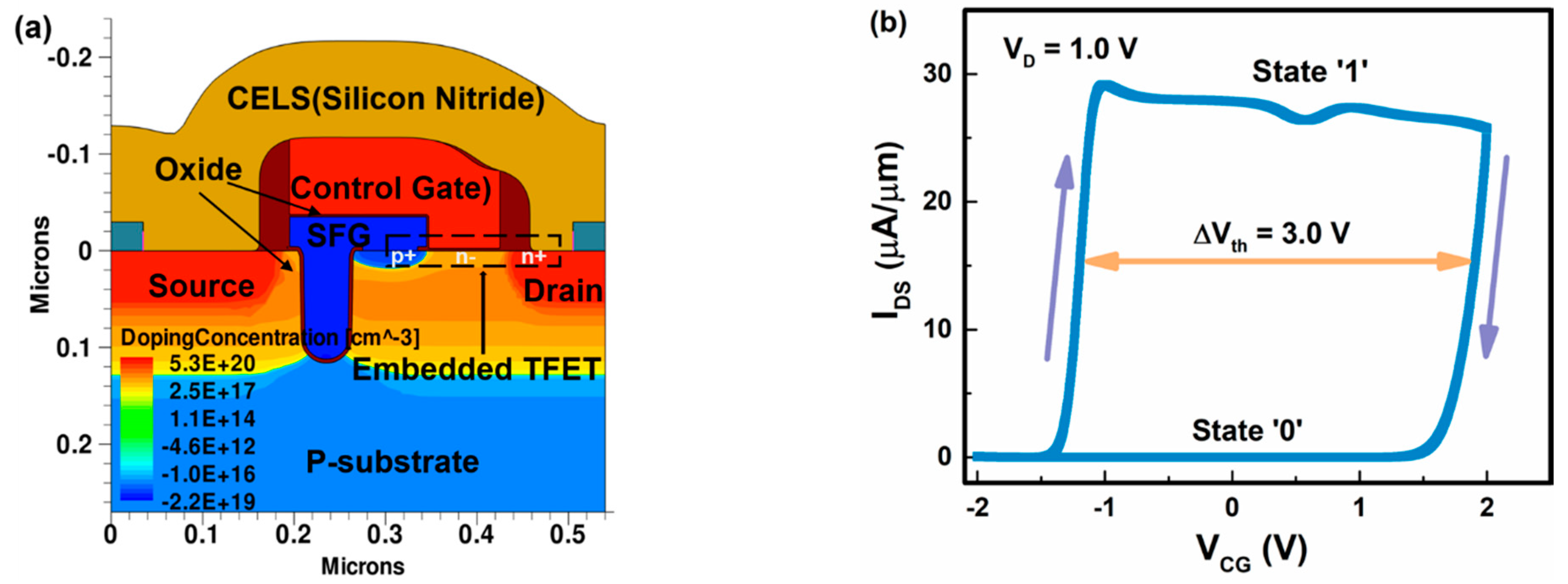
Figure 1. (a) Schematic of the U-shaped semi-floating gate transistor (SFGT) structure with tensile Si3N4 capper layer (CELS) and the doping contour used in the simulation; (b) The simulated transfer curve of the U-shaped SFGT device. The Vth has shifted 3.0 V when the device was switched between state 1 and state 0.
Electronics 08 00414 g001
Figure 2. (a) Contour of the band-to-band tunneling generation rate of the embedded field-effect transistor (TFET) during the write-1 operation; (b) Energy band diagrams along the horizontal cutline Y = 0.002 μm shown in (a). The band-to-band tunneling occurs in the place where the band bending is strongest that electrons tunnel from the valence band of the inverted channel to the conduction band of the n+ drain region.
Electronics 08 00414 g002
Figure 3. (a) The dependence of ΔEP of the semi-floating gate (SFG) on VCG during the write-1 operation; (b) The relation between the ΔEP of the SFG and the writing time for write-1 operation. VCG is −1.4 V and VD is 2 V.
Electronics 08 00414 g003
Figure 4. (a) Contour of stress XX along the channel direction; (b) Simulated drain current enhancement of SFGT memory with the tensive Si3N4 layer during a period of the operation sequence.
Electronics 08 00414 g004
Figure 5. (a) Retention performance of the U-shaped SFGT memory. The retention time is over 1 s; (b) Disturbance performance of the U-shaped SFGT memory. The immunity time to the worst disturbance mechanism can be up to 10 ms.
Electronics 08 00414 g005
Table 1. The operation condition of the U-shaped (semi-floating gate transistor) SFGT memory.
Write-1Write-0ReadStandby
VCG (V)−2.01.50.70
VD (V)1.40.61.41.0
Time (ns)5558