An Alternative Carrier-Based Implementation of Space Vector Modulation to Eliminate Common Mode Voltage in a Multilevel Matrix Converter


Abstract
:1. Introduction
2. Multilevel Matrix Converter
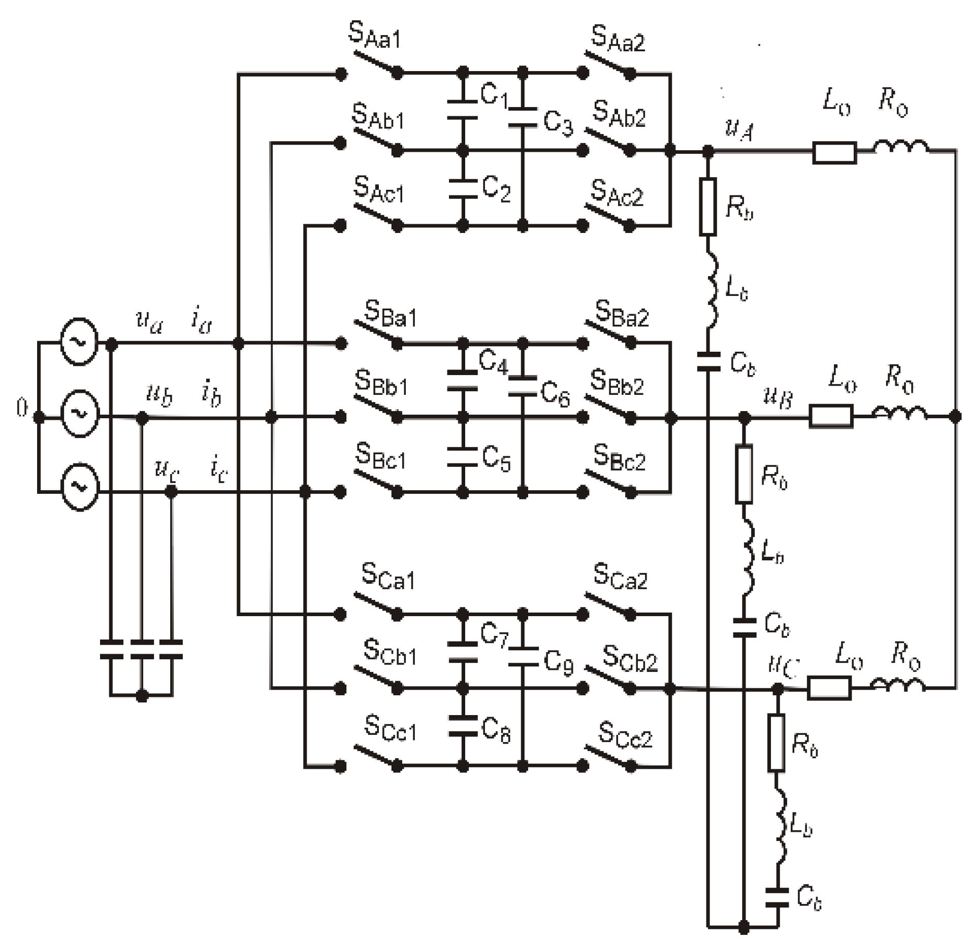
2.1. Topology of MMC
2.2. Admissible Switch Configurations of MMC
2.3. Output Voltage Space Vectors in MMC
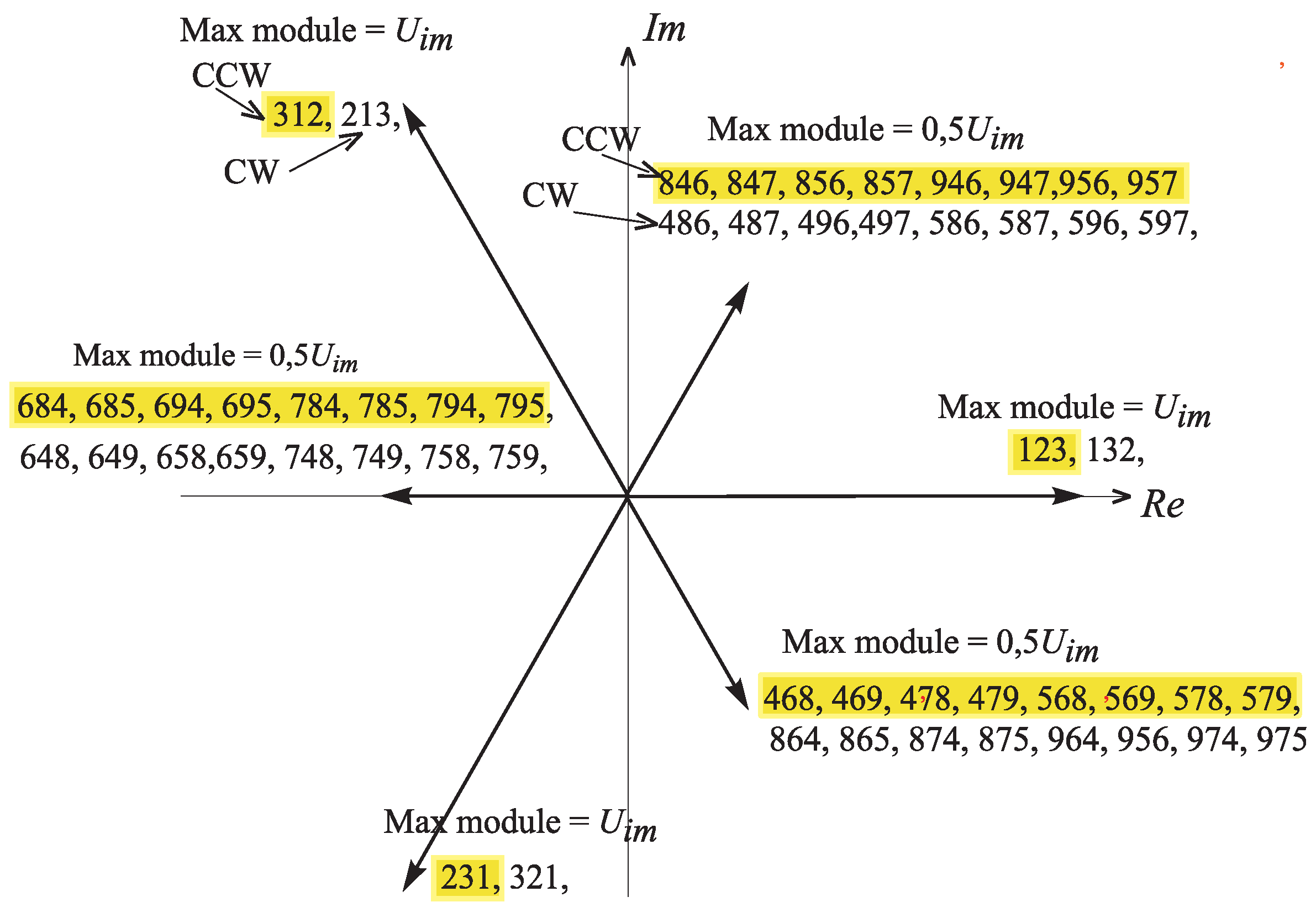
- 27 zero space vectors, where the output voltages in each phase are the same;
- 360 active space vectors, where two of the output voltages have the same values; and
- 342 rotating space vectors.
2.4. Output Voltage Space Vectors Reducing CMV in MMC
- Rotating voltage space vectors, with a constant module equal to the amplitude of the input voltage Uim. These vectors correspond to switch configurations, where three output voltages are synthesized by the use of three full-amplitude supplying voltages. Six vectors belonging to this group create two sets, consisting of three rotating space vectors shifted by 120º. One set rotates in a positive direction (CCW vectors) along a complex plane and the next set rotates in a negative one (CW vectors). Two of these vectors are represented by Equations (6) and (7), as well as the relation (6)—for CCW vectors and (7)—for CW vectors. The digits in the label of the voltage vector name should be interpreted as follows: the first digit defines the configuration of the switches in the output phase A, the second and third digits, the output phase B and C, appropriately. The application of the rotating space vectors belonging to this group in the modulation of switch duty cycles results in a zero value of CMV (8).where:
- Rotating voltage space vectors, with a constant module equal to half of the input phase voltage amplitude that corresponds to 48 configurations with a connection of three output phases to three different half-amplitude voltage supplies. Half of these vectors complete 8 sets of three vectors rotating in a positive direction (CCW vectors) and half of them form 8 sets of vectors rotating in a negative one (CW vectors). Two of these vectors are assigned as (9) (CCW vectors) and (10) (CW vectors). The application of the rotating space vectors belonging to this group in the modulation of switch duty cycles also results in a zero value of CMV (11).
- Rotating voltage space vectors, with a constant module equal to half of the input phase voltage amplitude, which corresponds to 72 configurations, with a connection of two output phases to two different half-amplitude voltage supplies and a third output phase connected to the full-amplitude voltage supply. Two examples are shown: CCW vector, as Equation (12) and CW vector, as Equation (13). The application in the modulation of switch duty cycles the rotating space vectors, belonging to the group being discussed, results in a value of CMV (14) that is not zero.
- Rotating voltage space vectors, with a changeable module, that correspond to 72 configurations, with a connection of two output phases to two different full-amplitude voltage supplies and a third output phase connected to a half-amplitude voltage supply. The Equation (15) is an example of the vectors belonging to this group. The application of the rotating space vectors, belonging to this group, in the modulation of switch duty cycles, results in a value of CMV (16) that is not zero.
- Rotating voltage space vectors, with a changeable module, that correspond to 144 configurations, with a connection of two output phases to two different half-amplitude voltage supplies and a third output phase connected to a full-amplitude voltage supply. The Equation (17) is an example of the vectors belonging to this group. The application of the rotating space vectors, belonging to this group, in the modulation of switch duty cycles, results in a value of CMV (18) that is not zero.
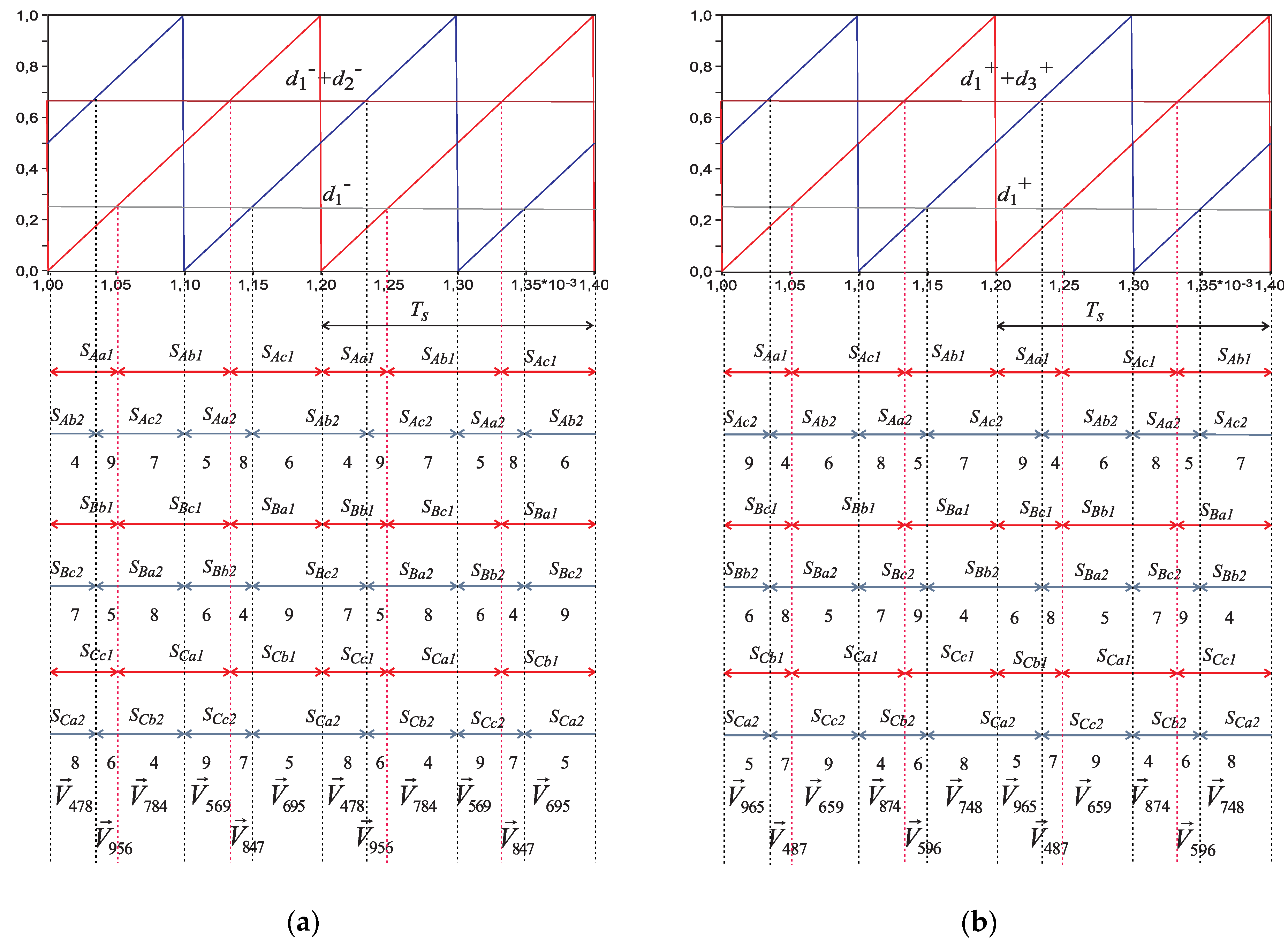
3. Proposed modulation method
Method of the Output Voltage Synthesis
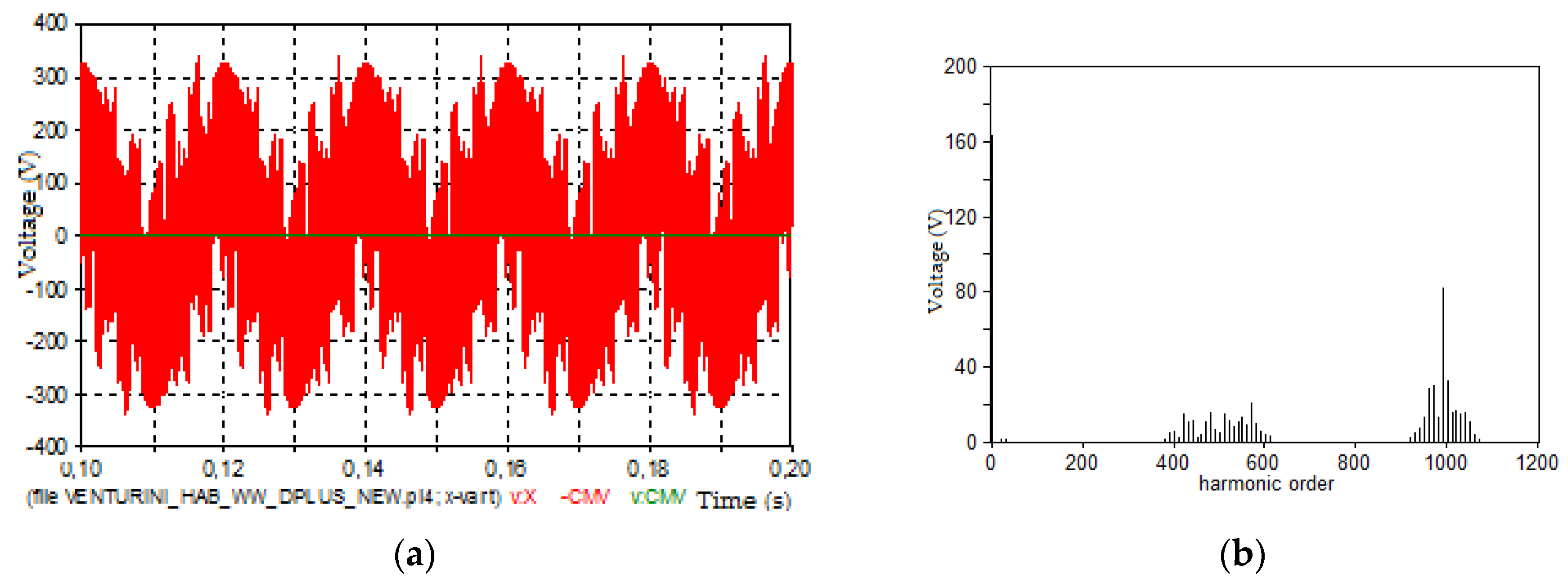
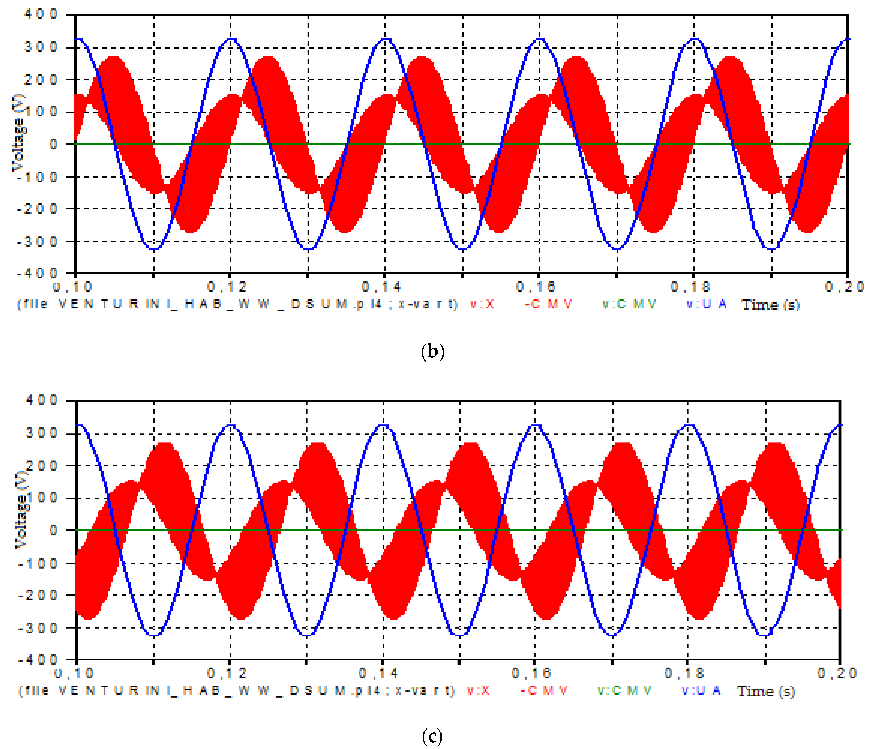
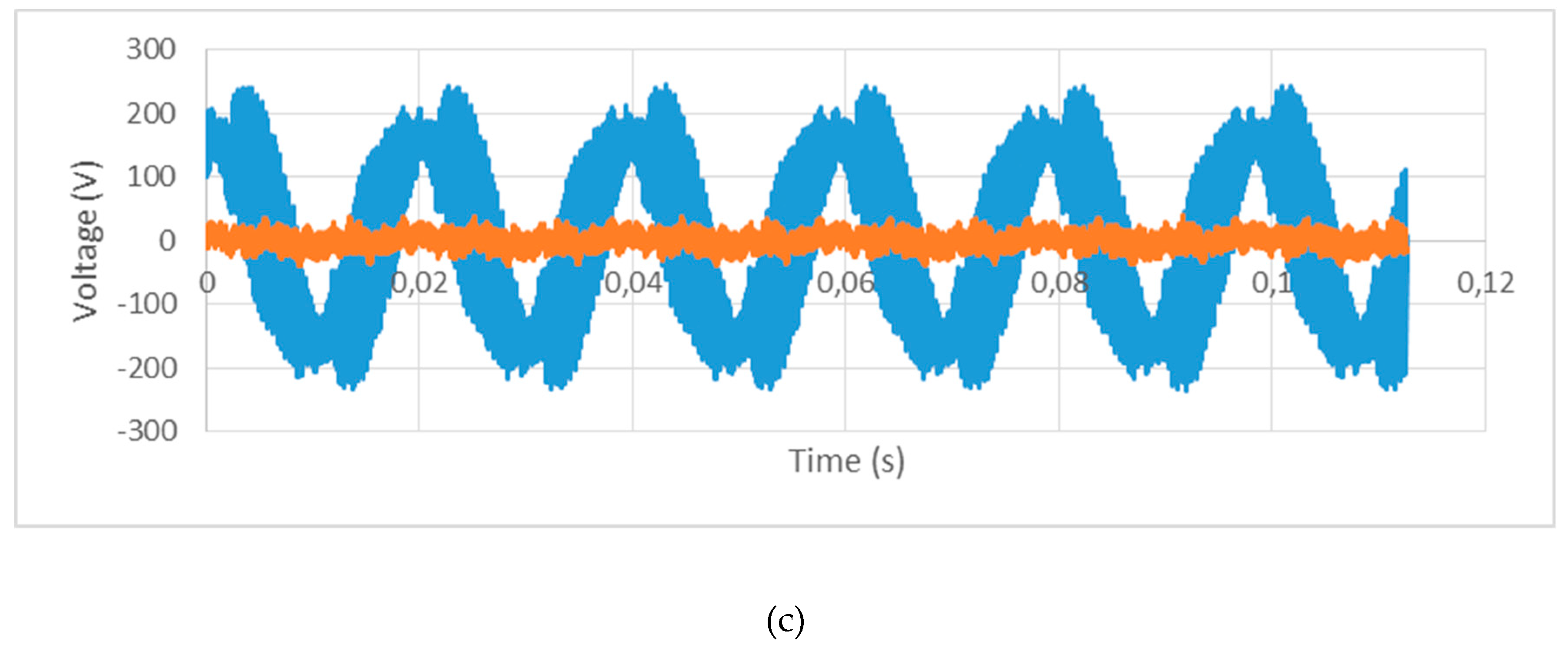
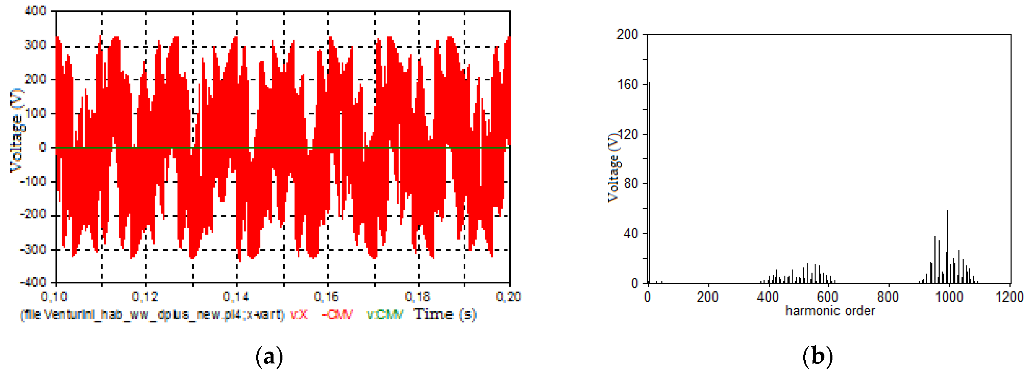
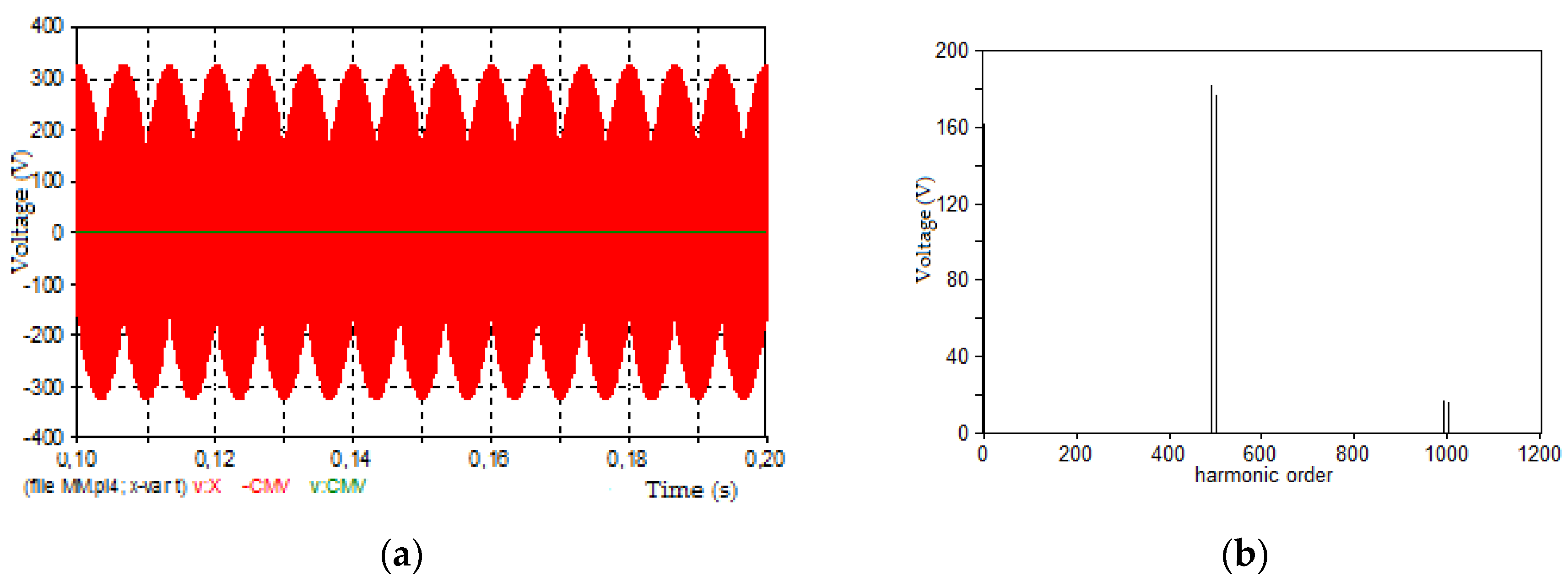
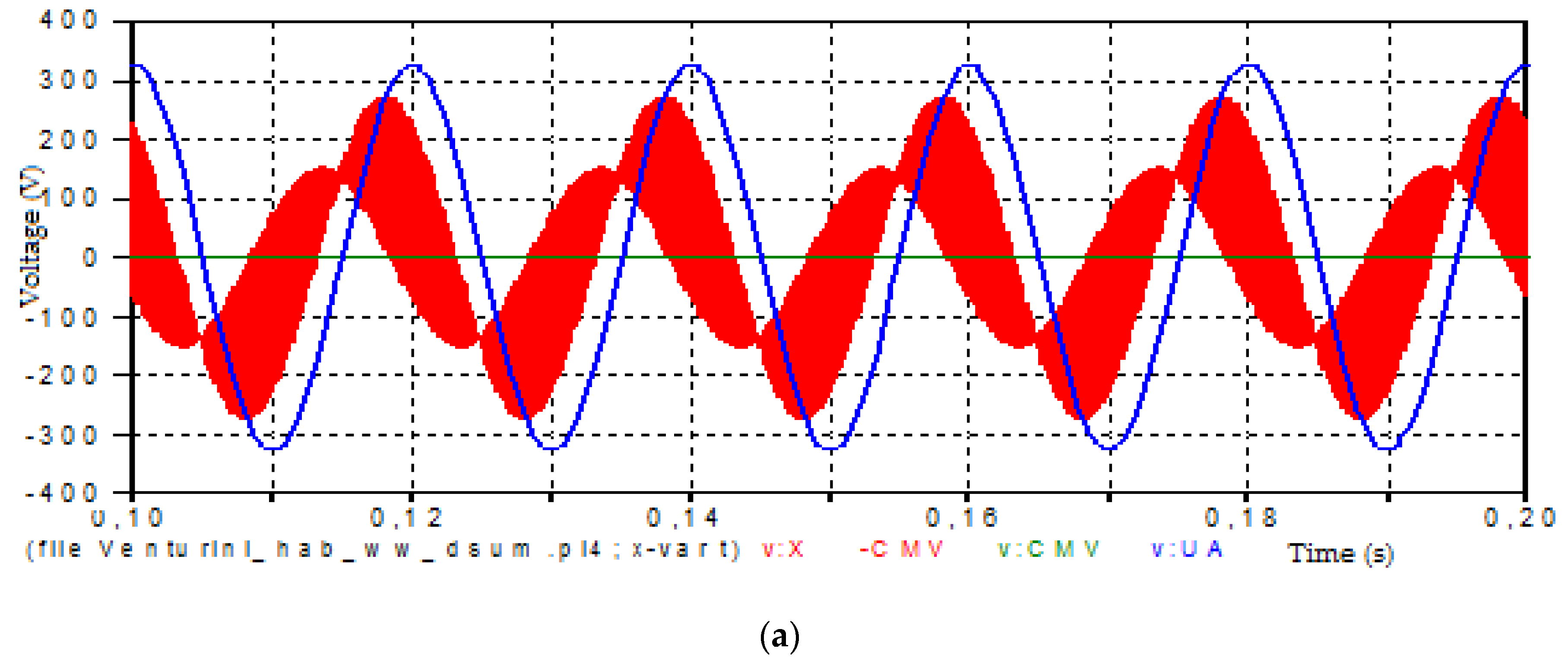
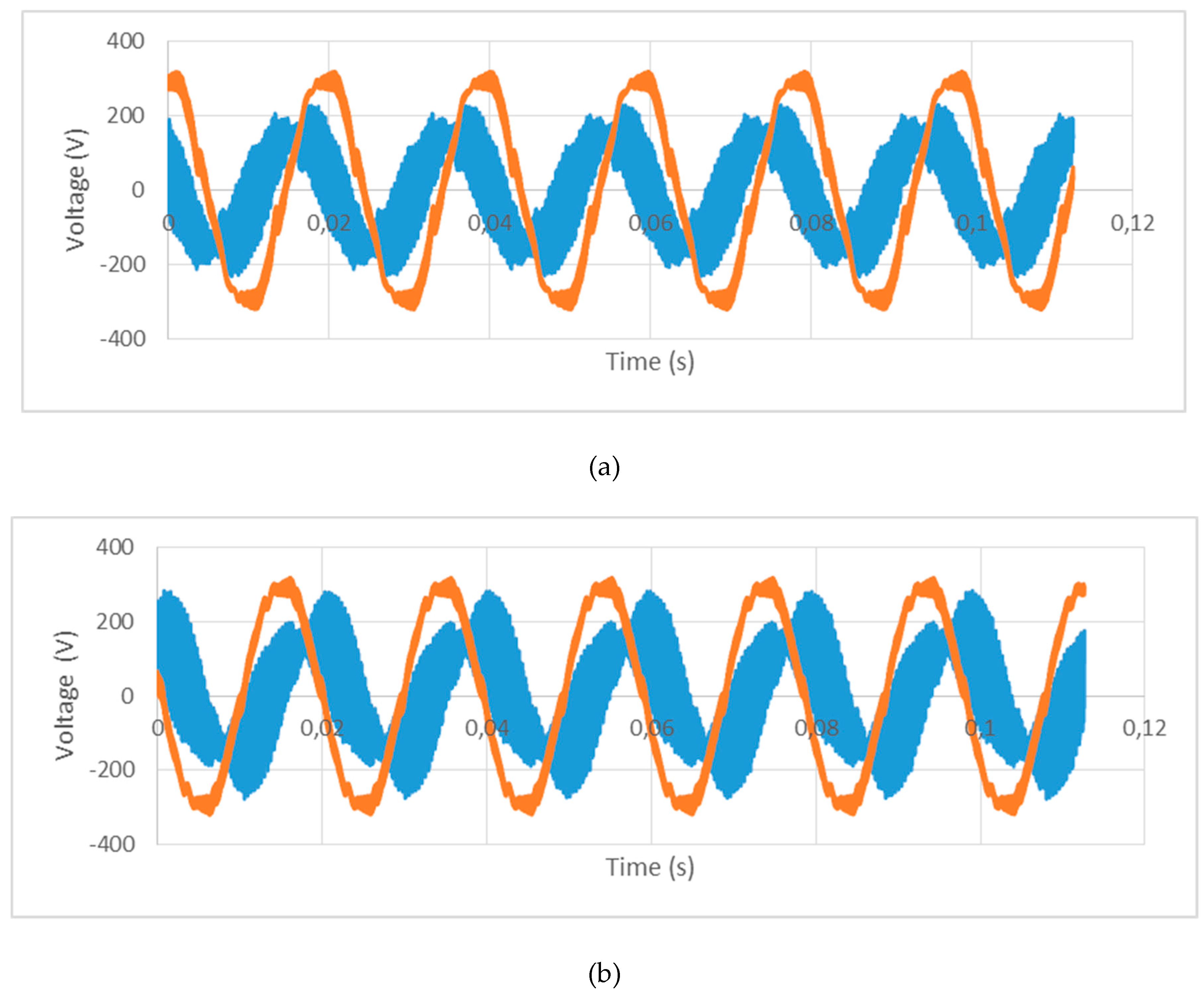
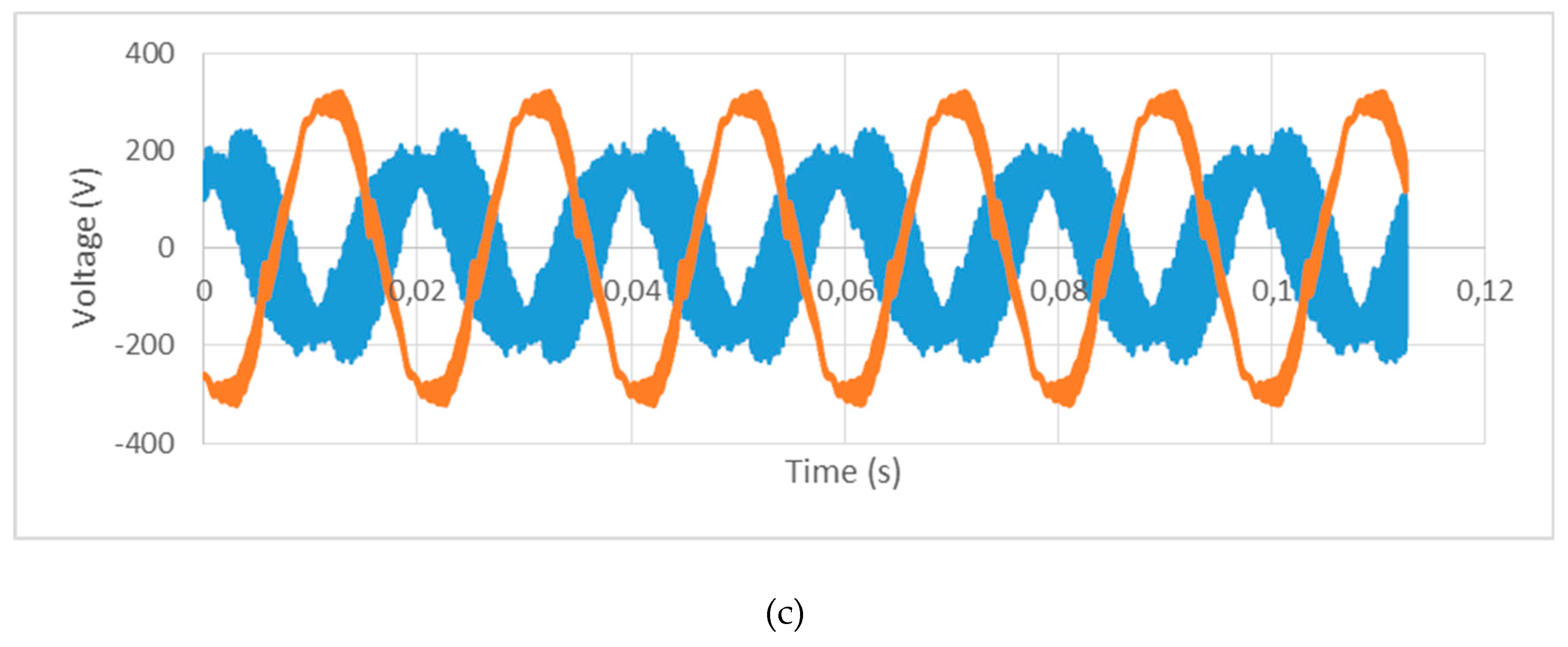
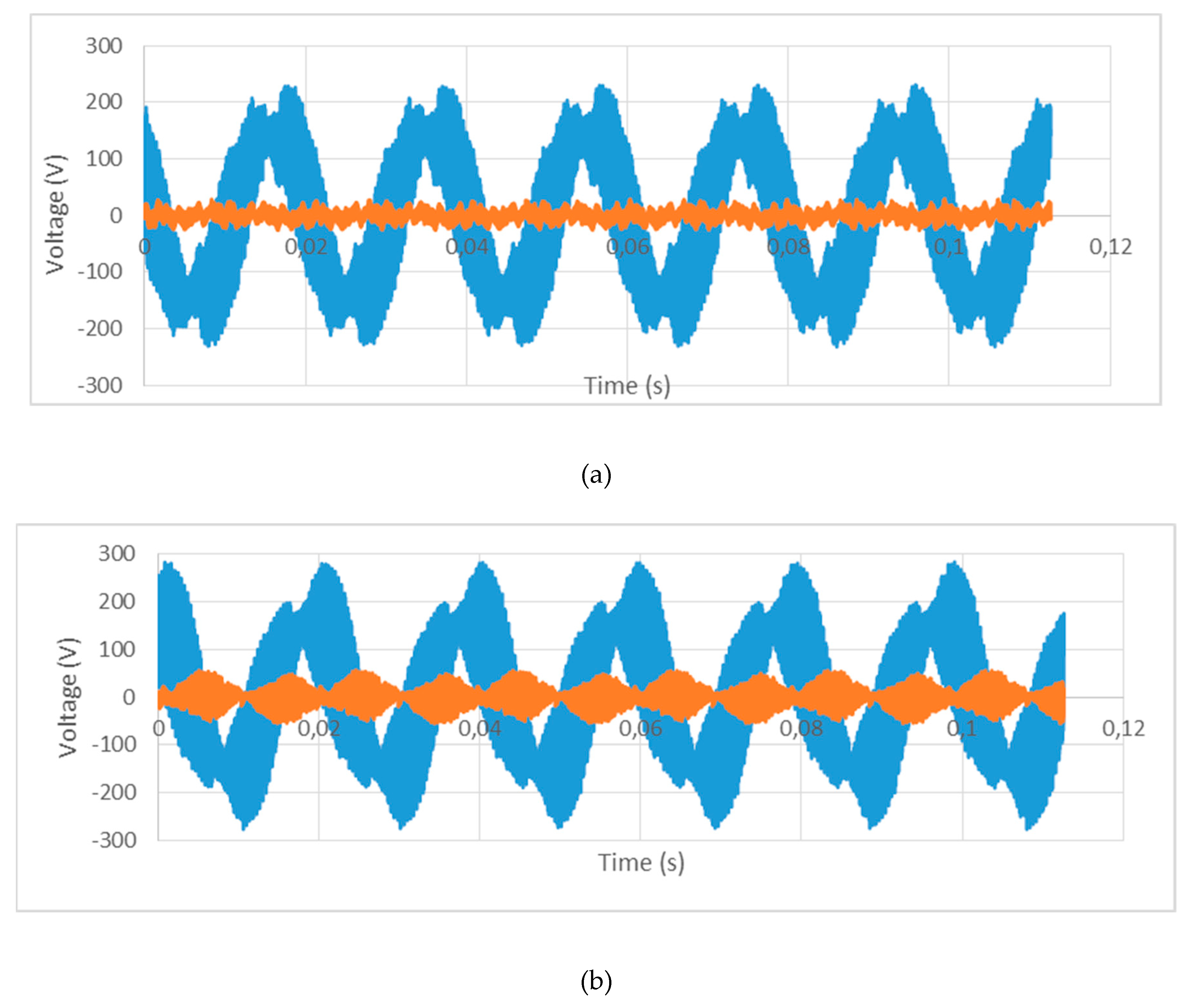
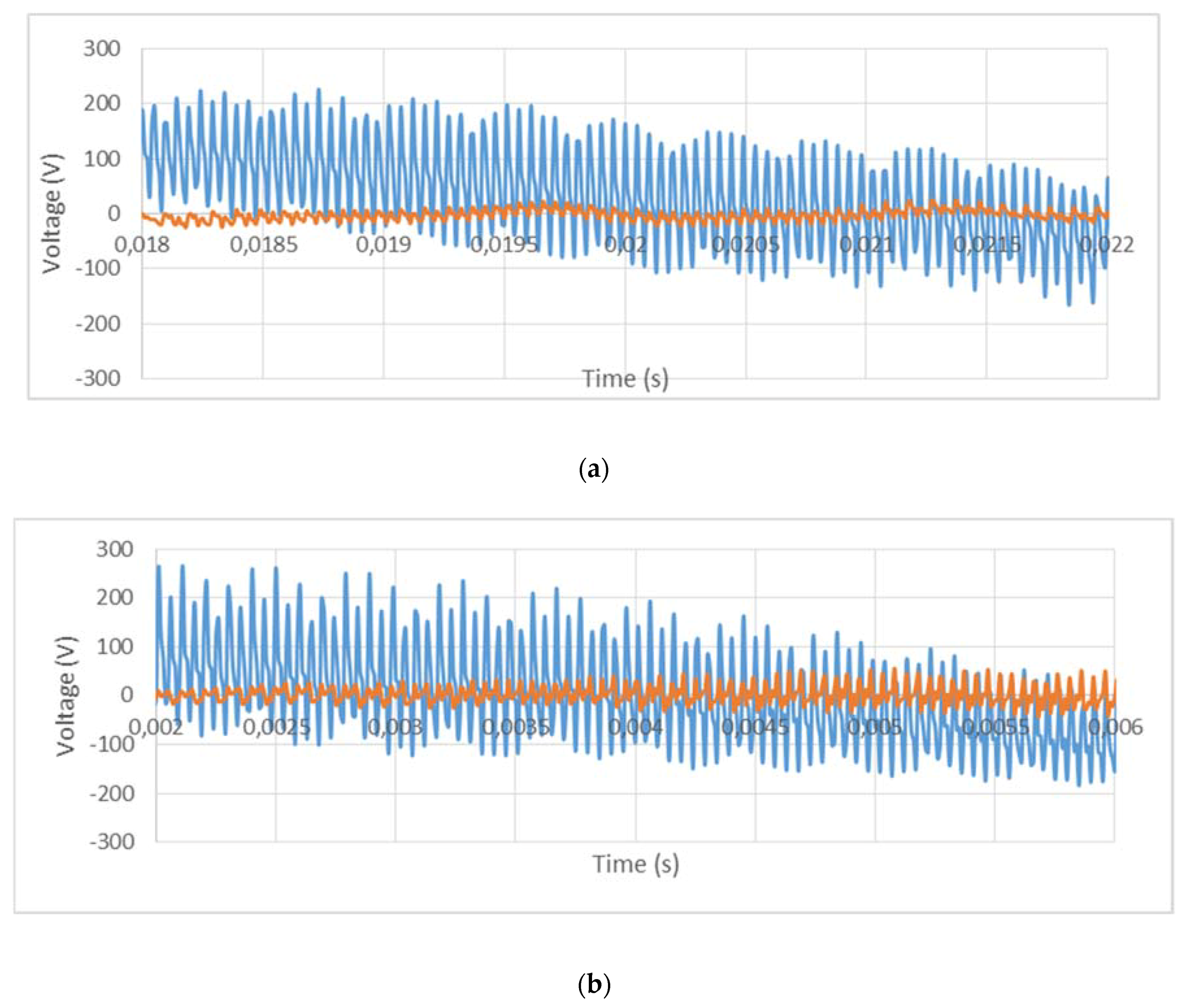
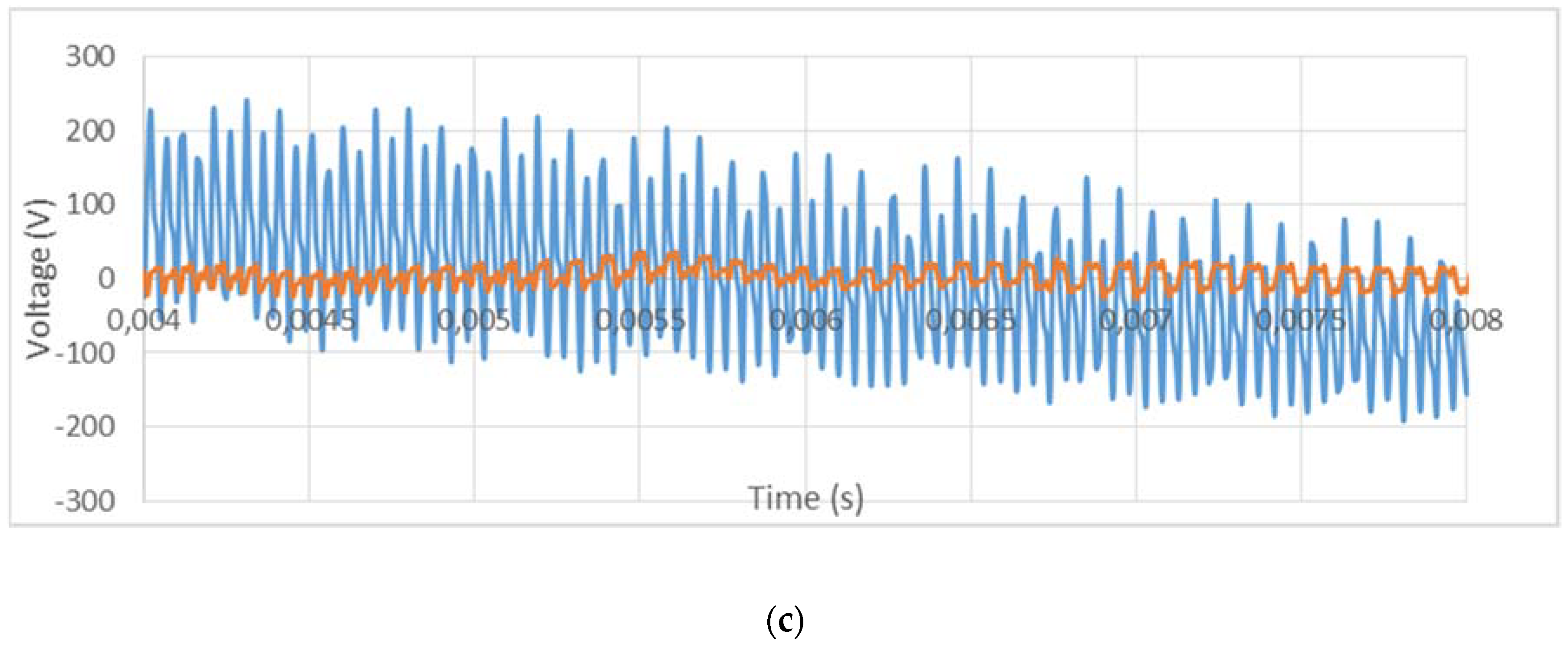
4. Simulation and Experiment
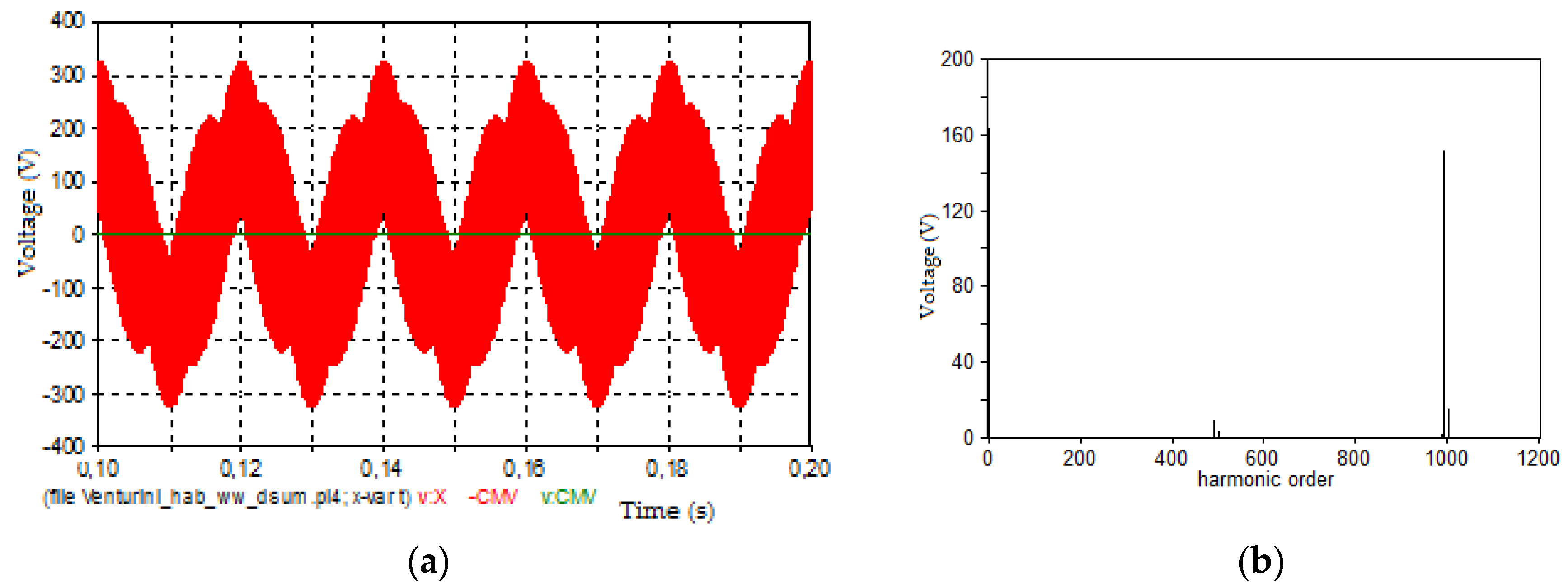
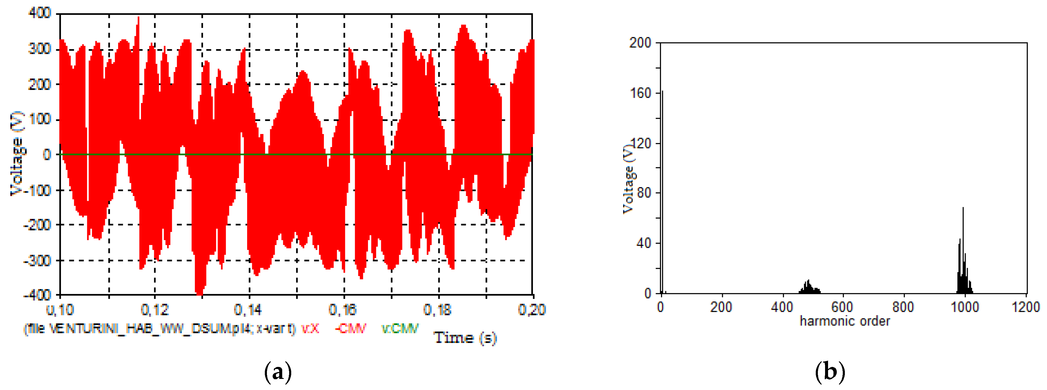
4.1. Simulation
4.2. Experiment
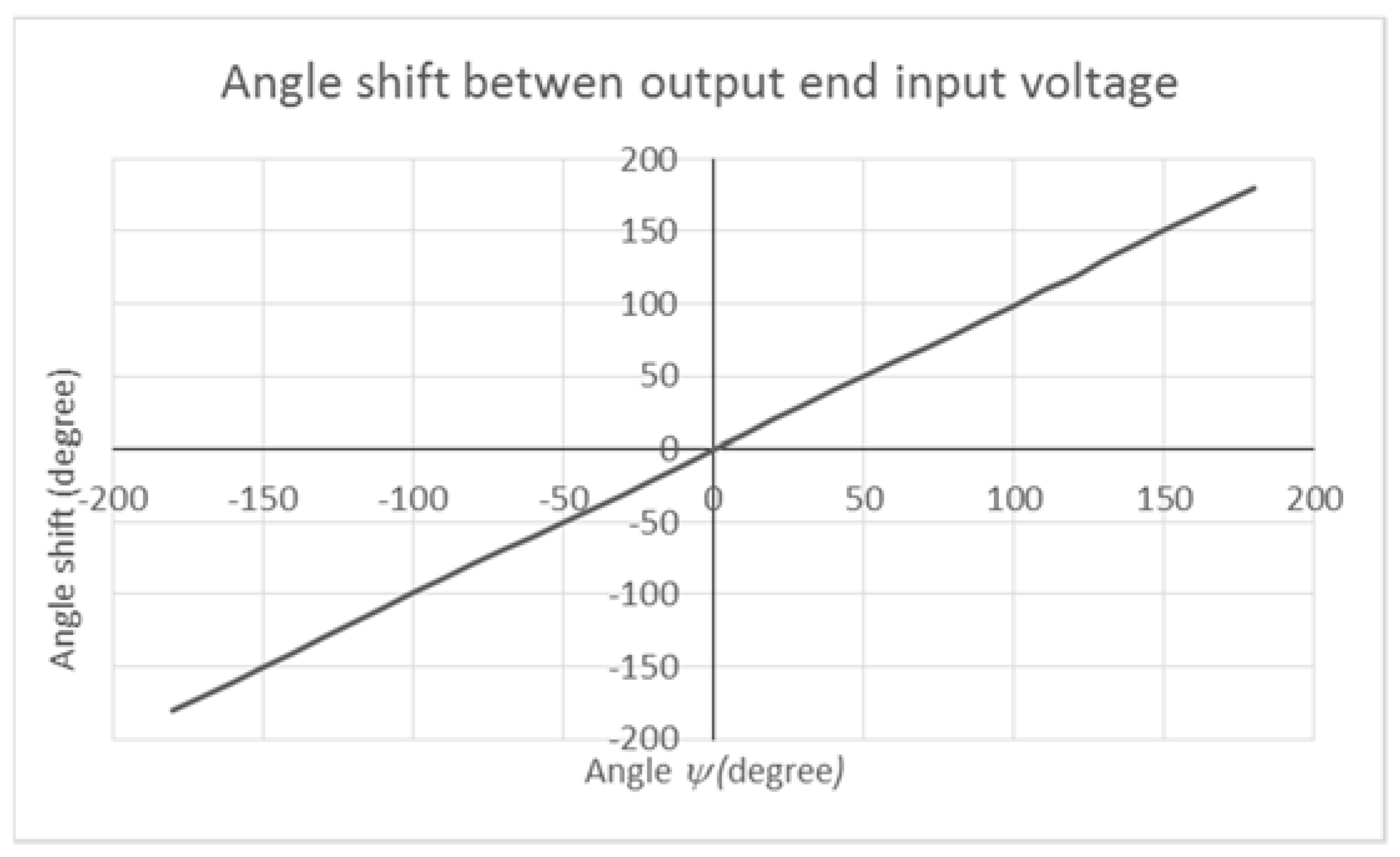
5. Discussion
Funding
Conflicts of Interest
Abbreviations
| AC | Alternating Current |
| CCW rotating space vector | Counter Clockwise rotating space vector |
| CMV | Common mode Voltage |
| CW | Clockwise rotating space vector |
| DC | Direct Current |
| EMTP-ATP | Electromagnetic Transients Program—with version ATP |
| FACTS | Flexible AC Transmission System |
| FFT | Fast Fourier Transformation |
| MC | Matrix Converter |
| MMC | Multilevel Matrix Converter |
| PWM | Pulse Width Modulation |
| SVM | Space Vector Modulation |
| VTR | Voltage Transfer Ratio |
References
- Shi, Y.; Yang, X.; He, Q.; Wang, Z. Research on Novel Capacitor Clamped Multilevel Matrix Converter. IEEE Trans. Power Electron. 2005, 20, 1055–1065. [Google Scholar] [CrossRef]
- Rząsa, J. Multilevel Matrix Converter Controlled with use of Venturini Method. Przegląd Elektrotechniczny Rok 2007, Nr 2, 57–64. (In Polish) [Google Scholar]
- Rząsa, J. Capacitor Clamped Multilevel Matrix Converter Controlled with Venturini Method. In Proceedings of the EPE-PEMC, Poznań, Poland, 1–3 September 2008. [Google Scholar]
- Rząsa, J. Switch Current Harmonic Distortion in Classic and Capacitor-Clamped Multilevel Matrix Converters. In Proceedings of the 35th Annual Conference of the IEEE Industrial Electronics Society IECON’09, Porto, Portugal, 3–5 November 2009. [Google Scholar]
- Lie, X.; Clare, J.C.; Wheeler, P.W.; Empringham, L. Space Vector Modulation for a Capacitor Clamped Multi-level Matrix Converter. In Proceedings of the EPE-PEMC 2008 13th International Power Electronics and Motion Conference, Poznań, Poland, 1–3 September 2008. [Google Scholar]
- Lie, X.; Clare, J.C.; Wheeler, P.W.; Empringham, L. Capacitor Clamped Multi-Level Matrix Converter: Space Vector Modulation and Capacitor Balance. In Proceedings of the 2008 34th Annual Conference of IEEE Industrial Electronics, Orlando, FL, USA, 10–13 November 2008. [Google Scholar]
- Lie, X.; Yongdong, L.; Kui, W.; Clare, J.C.; Wheeler, P.W. Research on the Amplitude Coefficient for Multilevel Matrix Converter Space Vector Modulation. IEEE Trans. Power Electron. 2012, 27, 3544–3556. [Google Scholar] [CrossRef]
- Lie, X.; Clare, J.C.; Wheeler, P.W.; Empringham, L.; Yongdong, L. Capacitor Clamped Multilevel Matrix Converter Space Vector Modulation. IEEE Trans. Ind. Electron. 2012, 59, 105–115. [Google Scholar] [CrossRef]
- Espina, J.; Ortega, C.; de Lillo, L.; Empringham, L.; Balcells, J.; Arias, A. Reduction of Output Common Mode Voltage Using a Novel SVM Implementation in Matrix Converters for Improved Motor Lifetime. IEEE Trans. Ind. Electron. 2014, 61, 5903–5911. [Google Scholar] [CrossRef]
- Espina, J.; Arias, A.; Balcells, J.; Ortega, C. Common mode output waveforms reduction for Matrix Converters drives. In Proceedings of the 2009 35th Annual Conference of IEEE Industrial Electronics, Porto, Portugal, 3–5 November 2009; pp. 4499–4504. [Google Scholar] [CrossRef]
- Guan, Q.; Wheeler, P.; Guan, Q.; Yang, P. Common-mode voltage reduction for matrix converters using all valid switch states. IEEE Trans. Power Electron. 2016, 31, 8247–8259. [Google Scholar] [CrossRef]
- Padhee, V.; Sahoo, A.K.; Mohan, N. Modulation technique for common mode voltage reduction in a matrix converter drive operating with high voltage transfer ratio. In Proceedings of the 2016 IEEE Applied Power Electronics Conference and Exposition (APEC), Long Beach, CA, USA, 20–24 March 2016; pp. 1982–1988. [Google Scholar] [CrossRef]
- Rzasa, J. Control of a matrix converter with reduction of a common mode voltage. In Proceedings of the IEEE Compatibility in Power Electronics, Gdynia, Poland, 6 January 2005. [Google Scholar]
- Nguyen, H.; Lee, H. A Modulation Scheme for Matrix Converters with Perfect Zero Common-Mode Voltage. IEEE Trans. Power Electron. 2016, 31, 5411–5422. [Google Scholar] [CrossRef]
- Mohapatra, K.K.; Ned, M. Open-End Winding Induction Motor Driven with Matrix Converter for Common-Mode Elimination. In Proceedings of the Power Electronics, Drives and Energy Systems, New Delhi, India, 12–15 December 2006. [Google Scholar]
- Gupta, R.K.; Mohapatra, K.K.; Somani, A.; Mohan, N. Direct-Matrix-Converter-Based Drive for a Three-Phase Open-End-Winding AC Machine with Advanced Features. IEEE Trans. Ind. Electron. 2010, 57, 4032–4042. [Google Scholar] [CrossRef]
- Tewari, S.; Mohan, N. Matrix Converter Based Open-End Winding Drives with Common-Mode Elimination: Topologies, Analysis, and Comparison. IEEE Trans. Power Electron. 2018, 33, 8578–8595. [Google Scholar] [CrossRef]
- Rząsa, J. Research on Dual Matrix Cnverter Feeding an Open-End-Winding Load Controlled with the Use of Rotating Space Vectors. Part I. In Proceedings of the 39th Annual Conference of the IEEE Industrial Electronics Society IECON 2013, Vienna, Austria, 10–13 November 2013. [Google Scholar]
- Rząsa, J.; Garus, G. Research on Dual Matrix Converter Feeding an Open-End-Winding Load Controlled with the Use of Rotating Space Vectors. Part II. In Proceedings of the 39th Annual Conference of the IEEE Industrial Electronics Society IECON 2013, Vienna, Austria, 10–13 November 2013. [Google Scholar]
- Baranwal, R.; Basu, K.; Mohan, N. An alternative carrier based implementation of Space Vector PWM for dual matrix converter drive with common mode voltage elimination. In Proceedings of the IECON 2014—40th Annual Conference of the IEEE Industrial Electronics Society, Dallas, TX, USA, 29 October–1 November 2014; pp. 1208–1213. [Google Scholar] [CrossRef]
- Jianglei, Q.; Lie, X.; Wang, L.; Lin, Q.; Yongdong, L. The modulation of common mode voltage suppression for a three-level matrix converter. In Proceedings of the 2016 IEEE International Conference on Aircraft Utility Systems (AUS), Beijing, China, 10–12 October 2016; pp. 533–538. [Google Scholar] [CrossRef]
- Jianglei, Q.; Lie, X.; Lina, W.; Yannian, H. Research on the modulation and control of multilevel matrix converter. J. Eng. 2018, 2018, 614–621. [Google Scholar] [CrossRef]
- Monteiro, J.; Silva, J.F.; Pinto, S.G.; Palma, J. Matrix Converter-Based Unified Power-Flow Controllers: Advanced Direct Power Control Method. IEEE Trans. Power Deliv. 2011, 26, 420–430. [Google Scholar] [CrossRef]
- Meynard, H.; Foch, T.A.; Thomas, P.; Courault, J.; Jakob, R.; Nahrstaedt, M. Multicell Converters: Basic Concepts and Industry Applications. IEEE Trans. Ind. Electron. 2002, 49, 978–987. [Google Scholar] [CrossRef]
- Meynard, T.A.; Fadel, M.; Aouda, N. Modeling of Multilevel Converters. IEEE Trans. Power Electron. 1997, 44, 356–364. [Google Scholar] [CrossRef]
- Pirog, S.; Stala, R. Selection of parameters for a balancing circuit of dc–dc and ac–ac multicell converters. In Proceedings of the 2005 European Conference on Power Electronics and Applications, Dresden, Germany, 11–14 September 2005; p. 910. [Google Scholar]
- Stala, R.; Mondzik, A. A study of the balancing process in multicell ac/ac converter. Przegląd Elektrotechniczny 2009, nr 7, 168–172. [Google Scholar]


| Switch State (‘on’: 1, ‘off’: 0) | Instantaneous Value of Voltage in Output Phase A | ||||||
|---|---|---|---|---|---|---|---|
| Configuration | SAa1 | SAa2 | SAb1 | SAb2 | SAc1 | SAc2 | |
| 1 | 1 | 1 | 0 | 0 | 0 | 0 | ua |
| 2 | 0 | 0 | 1 | 1 | 0 | 0 | ub |
| 3 | 0 | 0 | 0 | 0 | 1 | 1 | uc |
| 4 | 1 | 0 | 0 | 1 | 0 | 0 | (ua+ub)/2 |
| 5 | 0 | 1 | 1 | 0 | 0 | 0 | (ua+ub)/2 |
| 6 | 0 | 0 | 0 | 1 | 1 | 0 | (ub + uc)/2 |
| 7 | 0 | 0 | 1 | 0 | 0 | 1 | (ub + uc)/2 |
| 8 | 0 | 1 | 0 | 0 | 1 | 0 | (ua + uc)/2 |
| 9 | 1 | 0 | 0 | 0 | 0 | 1 | (ua + uc)/2 |
| Parameter Name | Parameter Value |
|---|---|
| clamp capacitors C1–C9 | 1.1 µF |
| balancing circuit Cb; Lb; Rb | 1 µF; 2.6 mH; 65 Ω |
| input frequency f | 50 Hz |
| RMS value of input phase voltage | 220 V |
| carrier frequency | 5 kHz |
© 2019 by the author. Licensee MDPI, Basel, Switzerland. This article is an open access article distributed under the terms and conditions of the Creative Commons Attribution (CC BY) license (http://creativecommons.org/licenses/by/4.0/).
Share and Cite
Rząsa, J. An Alternative Carrier-Based Implementation of Space Vector Modulation to Eliminate Common Mode Voltage in a Multilevel Matrix Converter. Electronics 2019, 8, 190. https://doi.org/10.3390/electronics8020190
Rząsa J. An Alternative Carrier-Based Implementation of Space Vector Modulation to Eliminate Common Mode Voltage in a Multilevel Matrix Converter. Electronics. 2019; 8(2):190. https://doi.org/10.3390/electronics8020190
Chicago/Turabian StyleRząsa, Janina. 2019. "An Alternative Carrier-Based Implementation of Space Vector Modulation to Eliminate Common Mode Voltage in a Multilevel Matrix Converter" Electronics 8, no. 2: 190. https://doi.org/10.3390/electronics8020190
APA StyleRząsa, J. (2019). An Alternative Carrier-Based Implementation of Space Vector Modulation to Eliminate Common Mode Voltage in a Multilevel Matrix Converter. Electronics, 8(2), 190. https://doi.org/10.3390/electronics8020190