Article

Development of a Hardware Simulator for Reliable Design of Modular Multilevel Converters Based on Junction-Temperature of IGBT Modules

Department of Electrical and Computer Engineering, Ajou University, 206, World cup-row, Yeongtong-gu, Suwon 16499, Korea
*
Author to whom correspondence should be addressed.
Electronics 2019, 8(10), 1127; https://doi.org/10.3390/electronics8101127
Submission received: 18 July 2019 / Revised: 23 September 2019 / Accepted: 1 October 2019 / Published: 7 October 2019
(This article belongs to the Section Power Electronics)

Abstract

:
This paper presents the development of a hardware simulator based on the junction-temperature of insulated-gate bipolar transistor (IGBT) modules in modular multilevel converters (MMCs). The MMC consists of various power-electronics components, and the IGBT is the main factor determining the lifetime of the MMC. The failure of IGBTs is mostly due to the junction-temperature swing; thus, the thermal profile of the IGBT should be established to predict the lifetime. The thermal behavior depends on the current flowing to the IGBT, and the load-current profile is related to the application. To establish the thermal profile of the IGBT, the proposed hardware simulator generates various shapes of output currents while the junction temperature is measured. Additionally, a controller design is presented for simulation of the arm current, which includes a direct current component as well as an alternative current component with a fundamental frequency. The validity and performance of the proposed hardware simulator and its control methods are analyzed according to various experimental results.

1. Introduction

Modular multilevel converters (MMCs) have been proven to be suitable for high-power conversion systems, such as high- and medium-voltage direct current (HVDC and MVDC, respectively) transmission systems [1,2,3,4]. The MMC has many advantages, such as low voltage stress in the switching device, a small amount of electromagnetic interference noise, and high output quality (close to an ideal sinusoidal output waveform) [5,6]. To improve the performance and efficiency of the MMC, numerous methods have been employed such as capacitor-voltage balancing control [7,8], modulation schemes [9,10], fault tolerance [11], thermal modeling [12], and lifetime-prediction modeling [13]. HVDC and MVDC systems using MMCs operate in harsh environments, because they are exposed to the outside; and operating the MMCs for a long time increases the probability of failure. Additionally, because the MMC is applied to high-power transmission and distribution systems, considerable financial costs per hour are incurred during restoration when the system is shut down. Therefore, the reliability of the MMC with regard to the lifetime, maintenance cost, and robustness is becoming a crucial issue.
The lifetime of a power-electronics system is determined by the characteristics of the system components such as the capacitor, gate driver, insulated-gate bipolar transistor (IGBT), etc. [14,15]. Of these, the IGBT is the main component that affects the lifetime of the entire system. The current flowing to the IGBTs determines the temperature variation, and the failure of the IGBTs depends on the thermal behavior [16,17,18,19,20]. The junction-temperature swing leads to repetitive thermomechanical stress in the IGBT module, which accumulates as fatigue on the device [15,21,22,23,24]. Therefore, the analysis of the thermal behaviors via the current flowing to the IGBT module is essential for the lifetime prediction. To predict the lifetime, it is necessary to estimate the junction temperature through mathematical thermal models.
In order to verify the feasibility of the thermal model, the simulator is required. Various simulators have been developed [24,25,26,27,28,29]. The simulators can operate close to the converter systems applied to real applications such as inductive loads and motors. In a conventional converter system such as a two- or three-level converter, which are used in a variety of applications, the current flowing to the IGBT module is composed of an alternative current (AC) component. Thus, most simulators are mainly applied to investigate the thermal behavior of the IGBT module according to the AC component. For the MMCs, the shape of current flowing to the IGBT is different from the typical inverter system. In contrast to the conventional converter, the arm current is composed of a direct-current (DC) component as well as an AC component [12,22]. Owing to the DC offset, the current flowing to each IGBT chip and diode in the IGBT module has a different shape and duration. This results in different thermal characteristics even though identical switching devices are used for the MMCs. Therefore, it is necessary to construct a simulator to analyze the thermal characteristics of the switching device depending on the arm current.
This paper proposes a hardware simulator for thermal profile analysis of the IGBT modules in the MMC. The proposed configuration can simulate the arm current of the MMC by controlling the DC and AC components independently, unlike conventional simulators, which are used to only simulate the AC component. The proposed simulator can also control the amplitude, the frequency of the simulated current and the power factor. Through the simulated current, the proposed hardware simulator can be employed to verify the thermal model applied to real MMC. The experimental results confirmed the validity and feasibility of the proposed simulator and its control method.

2. Reliability of the IGBT Module

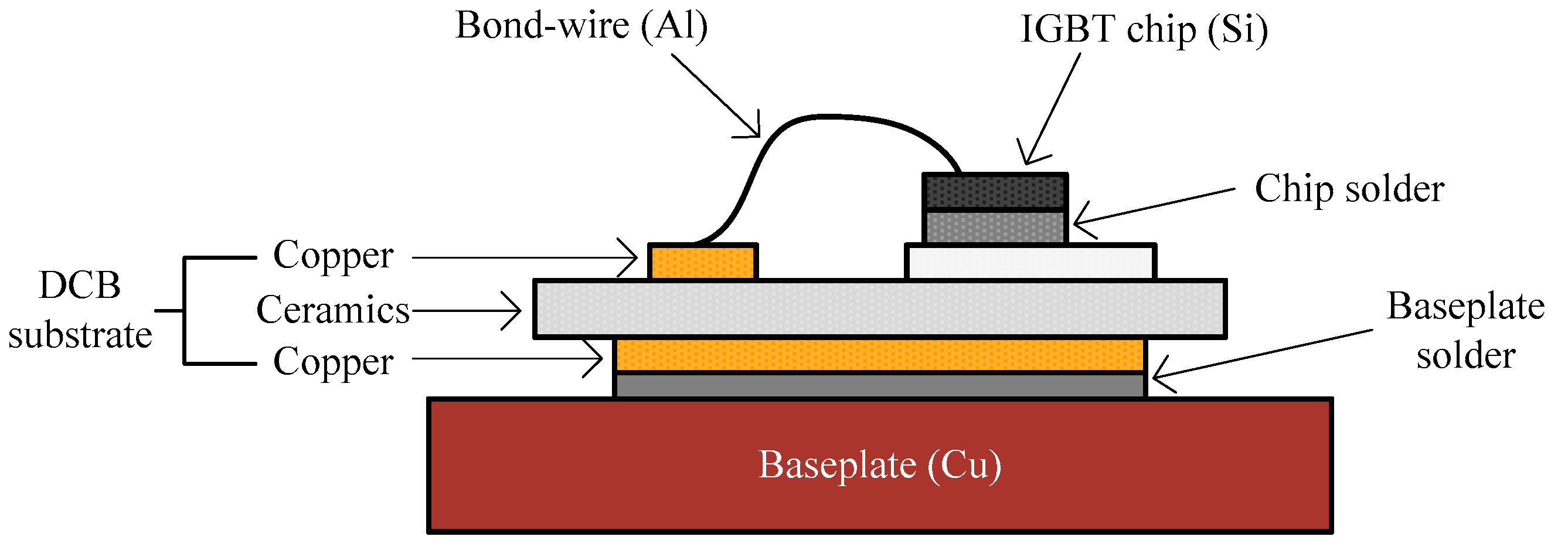
2.1. Cause of Failure in Standard IGBT Modules

Figure 1 shows the configuration of a standard IGBT module. The baseplate and IGBT chip are connected to the direct bond copper (DCB) substrate via soldering, and a bond wire is used to connect the emitter of the IGBT chip and the substrate [21]. When the current flows through the IGBT module, power losses occur, such as switching loss and conduction loss, and the power losses generate heat in the module. The periodical power loss or load variation causes a temperature variation in the IGBT module [15]. The repeated temperature variation in the IGBT module leads to thermomechanical stress and causes the liftoff or cracking of the bond wire, the reconstruction of the Al surface metallization, or solder-joint fatigue.
The failure of bond wires distorts the current flowing to the IGBT module and accelerates the bond-wire liftoff and the cracking of the remaining bond wires [22]. These failures lead to open-circuit failure or catastrophic failures of switching devices such as thermal runaway and semiconductor-chip destruction. The reconstruction of the Al surface metallization increases the resistance of the metal sheet owing to the rough metallization, non-uniform current distribution, and weakness of the connection between the metallization layer and bond wire [23]. Additionally, the temperature variation leads to solder-joint fatigue [21,23]. There are two solder joints in the standard IGBT module: between the IGBT chip and the DCB substrate and between the DCB substrate and the baseplate. Owing to the changes in the coefficient of thermal expansion caused by the temperature variation, thermomechanical stresses are applied to the solder joints, thus degrading the solder interface, e.g., causing cracks and delamination. Table 1 presents various failure mechanisms of the IGBT module. T and ∆T are the main causes of failure [15,22,23].

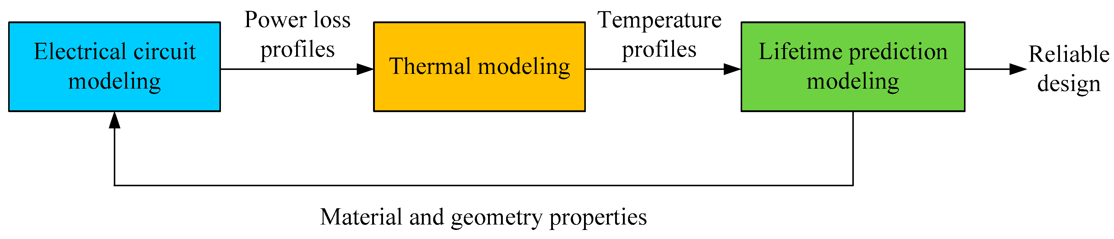
2.2. Process of Lifetime Prediction for the IGBT Module

Figure 2 shows the process of lifetime prediction for the IGBT module [21]. The characteristics of the current flowing to the IGBT module and the its thermal behavior depend on the application. Therefore, electrical-circuit modeling is needed to analyze the thermal characteristics of the IGBT module according to the application. Through electrical-circuit modeling, power loss profiles can be obtained based on load variations and the current flowing to the IGBT module. The thermal models of Cauer and Forster are well known and they are generally based on the junction temperature estimation [15,21]. The temperature profiles are established by substituting the power loss profiles into the thermal model. Based on the temperature profiles of the specific application, the lifetime of the IGBT module in the power converter can be estimated. The number of thermal cycles to failure can be determined by the temperature profiles and the thermal cycles determine the lifetime of the IGBT module [13,21]. The modeling of the lifetime prediction can be classified as empirical modeling and physics-based modeling. Empirical lifetime modeling is based on a large database of the junction temperature, which can be obtained via long-term experiments. The parameters related to the number of cycles to failure can also be obtained using the database of the junction temperature. Physics-based lifetime modeling utilizes the detailed physical and geometric characteristics of the IGBT modules. To determine the number of cycles to failure, the physical characteristics of the materials in the IGBT should be parameterized. Here, the thermal profiles are used for the parameterization. The lifetime-prediction model is used to improve the reliability of the IGBT modules and is applied to the design process for a reliable power-conversion system.
The proposed simulator can be employed to verify the thermal model applied to IGBT modules of real MMCs. In order to demonstrate the thermal model, it is necessary to compare the measured temperature with the estimated temperature obtained by thermal models such as the Cauer or Forster model. A verified thermal model can be applied under operating conditions in the actual MMC and thermal profiles can be obtained through the verified thermal model.

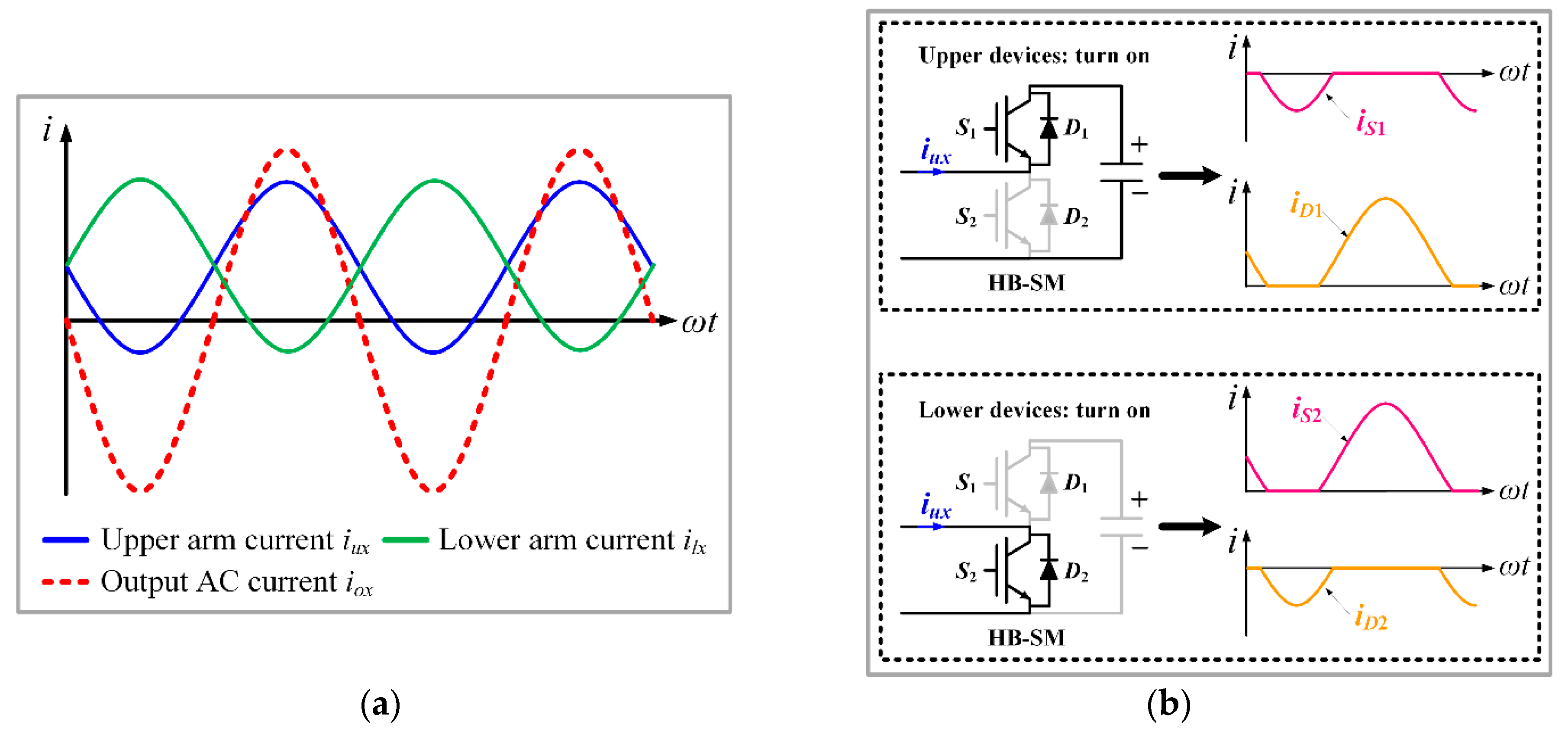
3. Modeling of Arm Current in MMC

Figure 3 shows the basic configuration of the three-phase MMC where VDC, IDC represent the DC-bus voltage and DC input current, and iux and ilx represent the upper- and lower-arm currents of x-phase (x = a, b, c), respectively. Each leg of the MMC is composed of two arms, and each arm consists of cascaded sub-modules (SMs) and an arm inductor Larm. Among the various candidates for the SM configuration, a half-bridge submodule (HB-SM) is most commonly applied because of its high efficiency and low cost. The phase current iox and the circulating current icc can be derived as iox = iuxilx and icc = (iux + ilx)/2, respectively. Thus, iux and ilx are expressed as follows:
i u x = i c c + i o x 2
i l x = i c c i o x 2
In the steady state, icc includes the DC component and the second-order harmonic, as follows:
i c c = I 2 f sin ( 2 ω o t + φ ) + I D C 3
where I2f represents the peak amplitude of the circulating current, ωo represents the fundamental frequency, and φ represents the initial phase angle of iox. If the second-order harmonic is relatively small or has negligible effects by elimination of the circulating current, then the arm currents iux and ilx can be derived as follows by substituting (3) into (4) and (5).
i u x = 1 3 I DC + 1 2 I AC sin ( ω o t + φ )
i l x =   1 3 I DC 1 2 I AC sin ( ω o t + φ )
where IAC represents the peak amplitude of the phase current. Figure 4a shows the upper-arm current iux and the lower-arm current ilx. The arm currents have the half-amplitude of IAC and a DC component. Therefore, the current wave is not located in the center vertically, indicating that the conducting current and power losses of the switching devices are not identically distributed.
The upper-arm current iux flowing to the switching devices in the HB-SM is shown in Figure 4b. In an SM, there are two IGBTs and two parallel diodes (labeled as S1, S2 and D1, D2, respectively). A different current flows to each switching device according to the direction of iux. If the upper switching devices are turned on and the lower switching devices are turned off, iux flows to D1 when its direction is positive and to S1 when its direction is negative. In contrast, if the lower switching devices are turned on and the upper switching devices are turned off, iux flows through S2 when its direction is positive and through D2 when its direction is negative. Because iux is composed of a DC component as well as an AC component, as shown in Figure 4a, the currents flowing to the switching devices do not have the shape of a half-sinusoidal waveform, and the duration of conduction differs. These characteristics indicate that the thermal behaviors of the switching devices in an HB-SM are different.

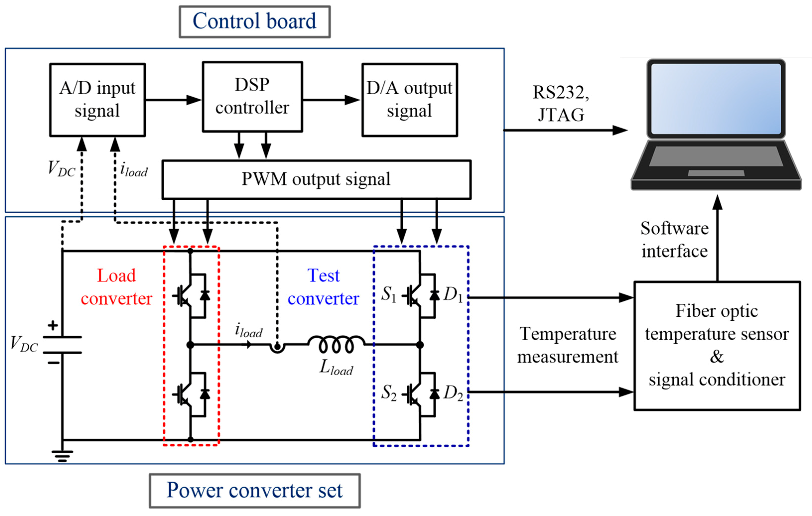
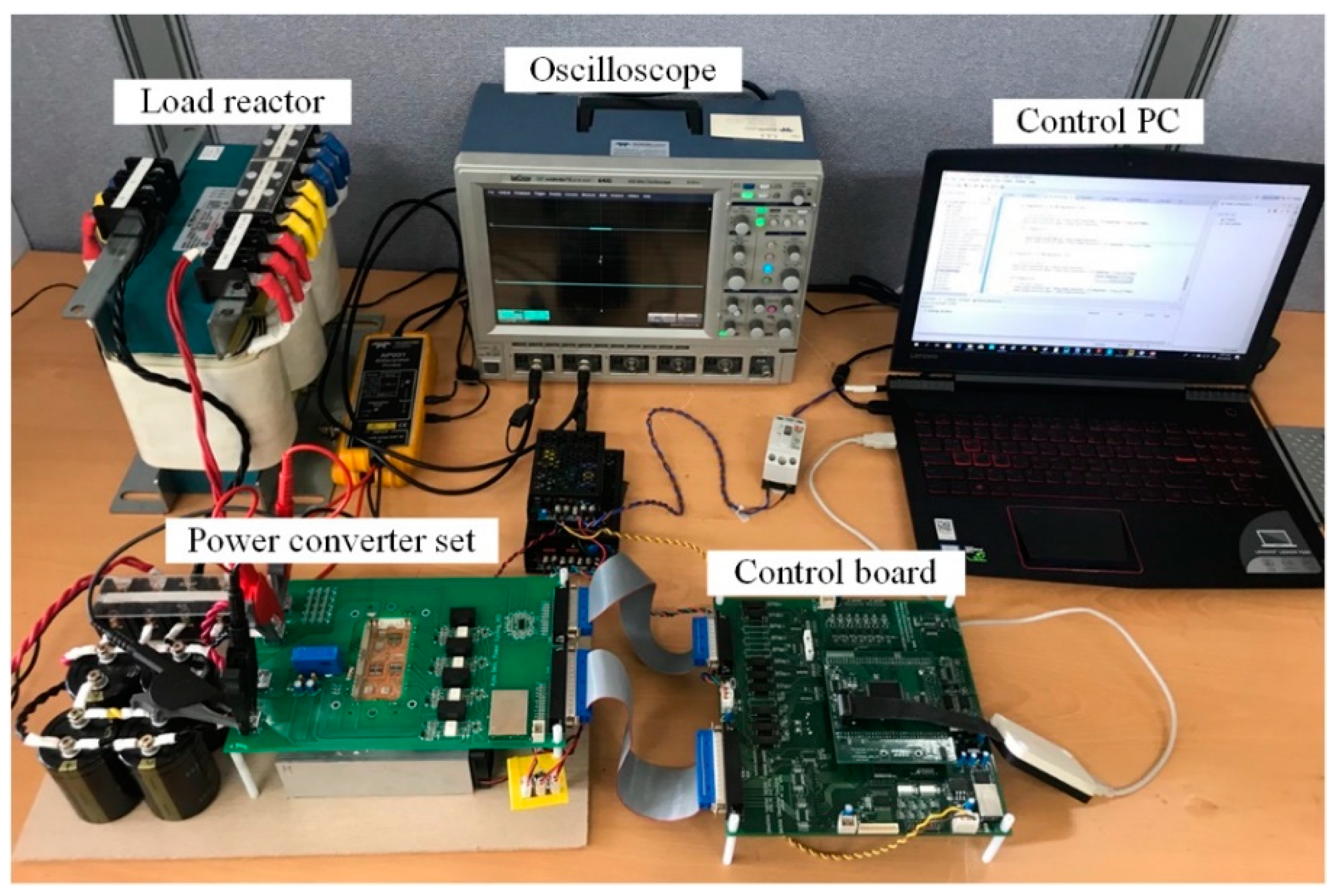
4. Design of Hardware Simulator

The temperature measurement is necessary to verify the accuracy and validity of the estimated temperature behavior obtained by the designed thermal model. Therefore, it is necessary to build a hardware simulator that can simultaneously simulate the load current and measure the temperature. This section provides details of the design of the proposed hardware simulator.
The configuration of the proposed simulator is shown in Figure 5. It consists of two half-bridge converters, a control board, a load reactor and temperature sensors. After removing gel inside the IGBT module, the temperature of the IGBT junction can be acquired by special instrumentation such as an IR camera or a fiber-optic sensor because insulation between the sensor and the power circuit is important for safe measurement. It is possible to effectively implement a temperature measuring experimental setup by using a fiber-optic sensor, which costs less than an IR camera.

4.1. Power-Converter Set

The power-converter set is composed of Lload, a DC-link capacitor, a test converter, and a load converter. Lload is connected between the output terminals of the test converter and load. Lload is utilized as a current path between the two converters. The test converter represents the target HB-SM of the MMC. The thermal characteristics of the IGBT in the test converter were analyzed under various load-current conditions. The load converter was configured with HB and generates the load current, which flows into the test converter through the load reactor. The generated load current can be controlled to have the same characteristics as the arm current in an actual MMC. Therefore, the load converter has the ability to control the amplitude, frequency, and power factor of iload. To design the two converters, F4-50R12KS4 from Infineon (1200 V/50 A) was used, because the package included two divided half-bridge legs. F4-50R12KS4 is composed of four IGBT chips and four diode chips. Figure 6a shows the F4-50R12KS4 module. The silicone gel inside the module was removed via a chemical process. The removal of the silicone gel is necessary to accurately measure the temperature using the fiber-optic temperature sensor. In order to operate F4-50R12KS4, the gate drivers named ACPL-332J from AVAGO were employed. ACPL-332J can produce output voltages of −9 V and 15 V. The power converter set can be applied to other semiconductor modules such as silicone carbide (SiC) and gallium nitride (GaN) because the output voltages of ACPL-332J are sufficient to operate these semiconductor modules. Figure 6b shows the designed power-converter board, on which F4-50R12KS4 was mounted. The board had a hall to expose the inside of the IGBT module. The power-converter board was connected to the control board for receiving the pulse-width modulation (PWM) signals and sending the measured parameters, such as the voltage, current, and temperature. The voltage and current were measured by sensors, and a negative-temperature coefficient thermistor provided the average temperature of the IGBT module. An aluminum heat sink and a fan named KA 9238HA2 were employed as the cooling system of the IGBT module in this study. The size of each were 120 × 150 × 50 and 92 × 92 × 38 mm, respectively. The cooling system was designed to keep the case temperature of F4-50R12K24 under 40 °C.

4.2. Load Reactor

One of the advantages of the MMC is that it is possible to implement a high output equivalent switching frequency feq from a low switching frequency fsw of each SM. Therefore, low total harmonic distortion (THD) of iox can be obtained, and the volume of the filter reactor can be reduced. The equivalent switching frequency feq is determined according to the modulation scheme and the number of SMs, N. Equations (6) and (7) indicate the equivalent switching frequency of the output voltage for two types of modulation methods: N + 1 and 2N + 1 phase-shifted PWM, respectively.
f e q ( N + 1 ) = N f s w
f e q ( 2 N + 1 ) = 2 N f s w
In practical applications of MMCs such as the HVDC and MVDC systems, each arm is composed of numerous SMs. Therefore, a high equivalent switching frequency can be obtained even though the device switching frequency is low. However, because the proposed simulator considers only one SM, the equivalent switching frequency is equal to the switching frequency of the test converter and the load converter. Therefore, the switching frequency should be selected with a high-speed frequency to realize the low THD of the load current, similar to that of actual MMCs. The load reactor is also designed to achieve a low THD of the load current with the selected switching frequency. For the proposed hardware simulator, the switching frequency was set as 10 kHz for both converters and the inductance of the load reactor was designed as 2 mH to achieve 2% of THD. The load reactor is composed of the copper coil and has the following specifications: a rating current of 40 A, and size of 195 × 300 × 230 mm. It is rather large because this reactor consists of three reactors, which are set as 1, 2 and 3 mH, respectively.

4.3. Control Board

To control the proposed hardware simulator, the control board employs a digital signal processor (DSP; TMS320F28335, Texas Instruments) and other peripheral circuits. TMS320F28335 is a high-performance controller with 150-MHz clocks, 12 ports for the PWM output, 16 channels for the analog-to-digital converter (ADC), etc. The DSP is interfaced with a personal computer through JTAG serial communication. The proposed hardware simulator requires four ports of PWM to drive the test converter and load converter. Additionally, three ADC ports are needed to receive information regarding the DC-link voltage, load current, and temperature of the IGBT module.

4.4. Fiber-Optic Temperature Sensor

Figure 7a shows the fiber-optic temperature sensor, which is mounted to the junction of the IGBT chip. The junction temperature can be measured through direct contact between the tip of the fiber-optic sensor and the switching devices of the IGBT module. To reduce the influence of the thermal coupling, the temperature of the switching devices was measured close to it and the silicone gel that covers the IGBT chip and diode was removed. The signal conditioner analyzes the received analog data from the tip regarding the junction-temperature swing, as shown in Figure 7b. The temperature-swing curves were checked using a software interface. As shown in Figure 7b, light is injected from the signal conditioner to the GaAs crystal at the end of the optical cable. The GaAs crystal absorbs the light with wavelengths below the bandgap spectral position and reflects the light with wavelengths above the bandgap to the signal conditioner. The light reflected to the signal conditioner is transferred to the optical spectrum analyzer to obtain the temperature information. In this study, the fiber-optic sensor OTG-F from Opsens Co. was employed; it has a sampling time of 5 ms, an accuracy of ±0.3 °C, and a resolution of 0.05 °C. The measurement range is from −40 to 250 °C. Due to sampling time restrictions of the optic fiber sensor, the thermal behavior of the IGBT module should be investigated with low fundamental frequency of the current. If the fundamental frequency is 50 Hz, just four samples of the temperature can be obtained. Therefore, the hardware simulator should perform the control ability for various fundamental frequencies and amplitude. The control strategy of the proposed hardware simulator is described in the following section.

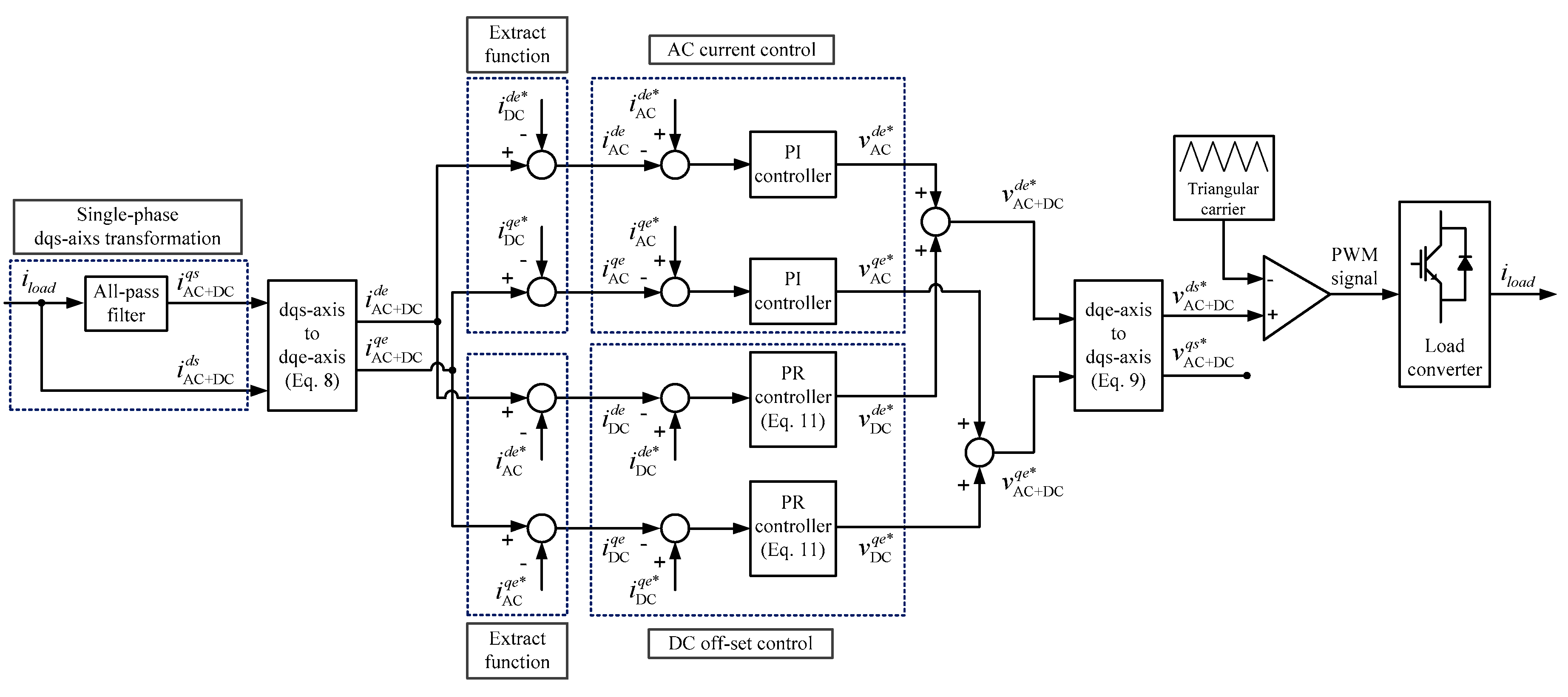
5. Design of Arm Current Controller

In MMCs, the arm current flowing to the SMs includes a DC component, as indicated by (4) and (5). This is a distinctive characteristic of the arm current generated by MMCs compared with to other power converters. Because the DC component causes different thermal behavior in IGBTs compared with other topologies, the simulator should provide the ability to control the AC and DC components for simulating the arm current of actual MMC systems. As mentioned previously, the fiber-optic sensor provides a 5 ms sampling time. It is necessary that the simulator generates the output current with a low fundamental frequency to obtain as many temperature samples as possible during a fundamental period. This paper proposes control strategies for various load-current conditions.
Figure 8 shows a block diagram of the proposed current controller for the hardware simulator. The load current iload is composed of an AC component and a DC component. It is converted into the current on the synchronous reference frame (dqe-axis), which rotates with the fundamental frequency. The transformation matrix from stational reference frame (dqs-axis) to dqe-axis can be expressed as Equation (8).
[ i AC + DC d e i AC + DC q e ] = [ cos ( ω t ) sin ( ω t ) sin ( ω t ) cos ( ω t ) ] [ i AC + DC d s i AC + DC q s ]
where i A C + D C d e and i A C + D C q e represent de-axis and qe-axis currents; i A C + D C d s and i A C + D C q s represent ds-axis and qs-axis currents, respectively; and ω represents the fundamental frequency of iload. The transformed AC component, i A C d q e , and DC component, i D C d q e , have physical DC and AC values, respectively. To extract i A C d q e and i D C d q e from the transformed current i A C + D C d q e individually, the reference values of the DC and AC components ( i A C d q e * and i D C d q e * ) are subtracted from i A C + D C d q e , respectively. The extracted AC component i A C d q e is compared with its reference value i A C d q e * and the error between them is controlled to be zero using a proportional-integral (PI) controller. The extracted DC component current i D C d q e is controlled using a proportional-resonant (PR) controller.
The sum of each controller output on the dqe-axis ( v A C + D C d e * and v A C + D C q e * ) transforms the dqs-axis value ( v A C + D C d s * and v A C + D C q s * ). Equation (9) indicates the transformation matrix from dqe-axis to dqs-axis.
[ v AC + DC d s * v AC + DC q s * ] = [ cos ( ω t ) sin ( ω t ) sin ( ω t ) cos ( ω t ) ] [ v AC + DC d e * v AC + DC q e * ]
v A C + D C q s * becomes the voltage reference of the load converter compared with the triangular carrier, which is applied to a gating signal to the switching devices of the load converter. Finally, the dqe-axis current i A C + D C d q e , which is composed of the DC and AC components, is generated on the load reactor. Each controller is described in detail below.

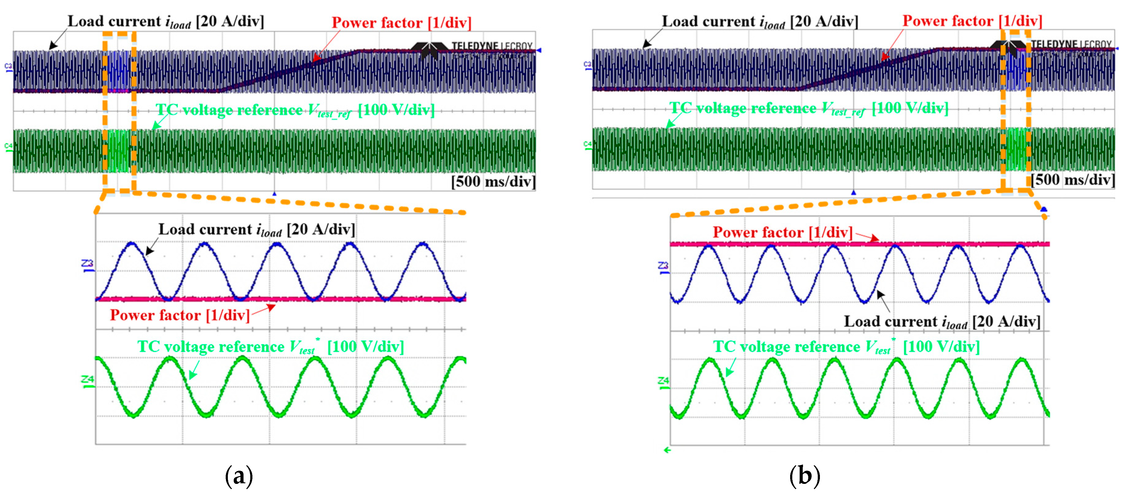
5.1. Control of AC Component

The current control for the AC component is based on the PI controller for simulating various conditions, such as the amplitude, frequency, and power factor. Because the steady-state error of the PI controller can be controlled to zero when the input variable is the DC value, the AC component should be expressed as a physical DC value on the dqe-axis. To transform the AC component into the value on the dqe-axis, the single-phase AC component should be expressed as dqs-axis components. Therefore, a virtual qs-axis current is required, and the fundamental AC component is set as the ds-axis current, i A C d s . The virtual qs-axis current, i A C q s , is a 90° delayed signal compared with i A C d s and can be obtained by using the all-pass filter, as shown in Figure 8. The dqs-axis currents are transformed into dqe-axis currents i A C d e and i A C q e . As mentioned previously, the arm current includes the DC component; thus, the AC component should be extracted for obtaining stable control results of the PI controller. By subtracting the reference value of the DC component i D C d q e * from i A C + D C d q e , the AC component on the dqe-axis i A C d q e can be obtained. The error between i A C d q e * and i A C d q e becomes the input for the PI controller. The gains of the PI controller are designed by modeling the voltage equation of RL-load. Because the load of the proposed simulator consists of only the reactor, the parameter R is considered to be a very small value: approximately 0.2 Ω. The output of the PI controller v A C d q e * is applied to the load reactor after it is converted into the dqs-axis variable and it generates the AC component of the load current. The de-axis current and qe-axis current represent the reactive and active currents, respectively. Therefore, the power factor of the output power can be easily adjusted by controlling the de- and qe-axis currents independently. Additionally, the fundamental frequency of the load current can be selected as an arbitrary value. By adjusting the fundamental frequency of the load current, the thermal behavior can be investigated, even if the sampling of the temperature sensor is slow.

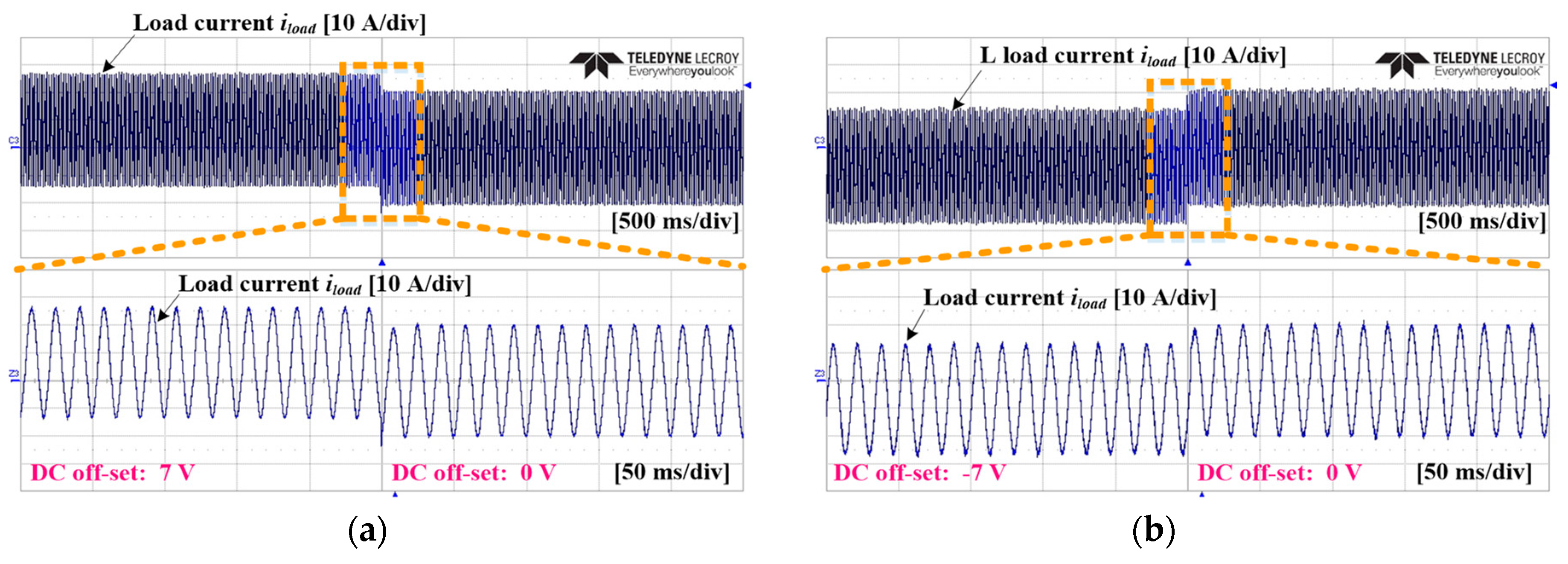
5.2. Control of DC Offset

As mentioned previously, the DC offset of the load current on the dqe-axis forms a physical AC value. To control the DC component, the PR controller was employed, because it is suitable for controlling physical AC values [30]. Equations (10) and (11) give the gains of the ideal PR controller (GI(s)) and the non-ideal controller (GNI(s)), respectively.
G I ( s ) = K P + 2 K R s s 2 + ω 2
G N I ( s ) = K P + 2 K R ω c s s 2 + 2 ω c s + ω 2
Here, KP represents the proportional gain, KR represents the resonance-frequency gain, ωc represents the cutoff frequency, and ω represents the resonance frequency of the current control system with the PR controller. The ideal PR controller provides a very high gain and narrow frequency bandwidth at the selected frequency. Therefore, it might cause stability problems. In comparison, the non-ideal PR controller exhibits a low gain. However, it is adequate for reducing the steady-state error sufficiently and ensuring stability owing to the wide bandwidth at the selected frequency. The control strategy for the DC offset involves the same sequence as the AC component control strategy.

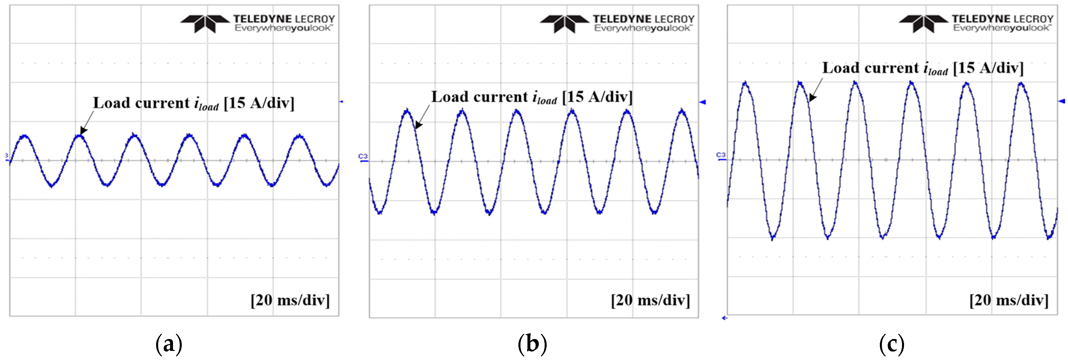
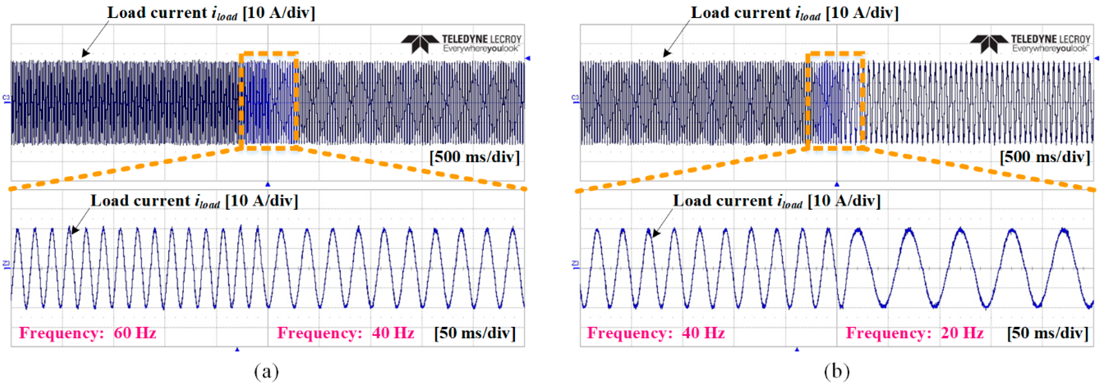
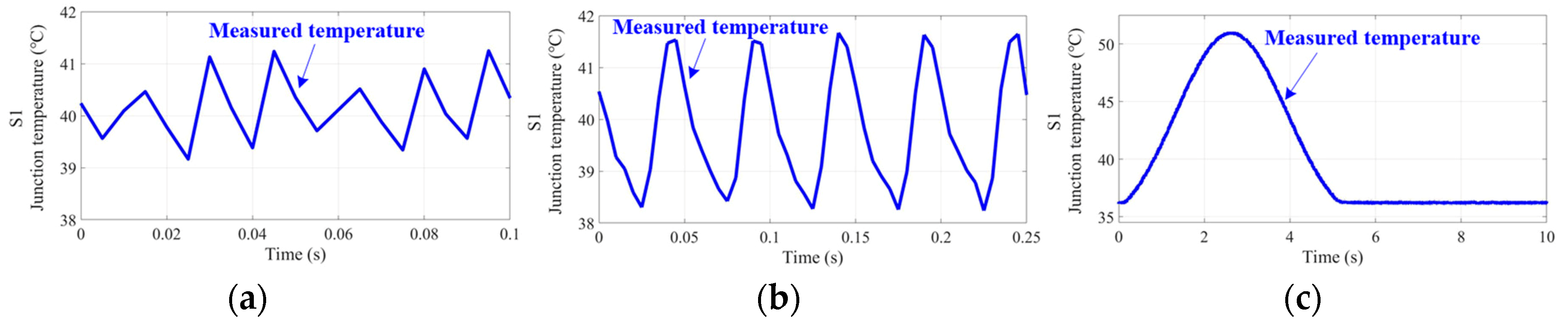
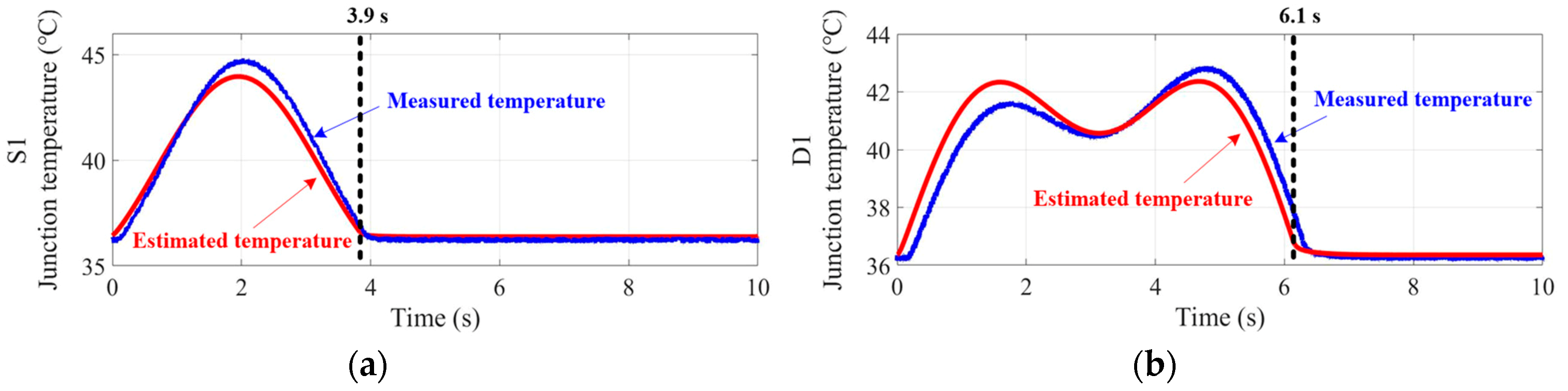
6. Experimental Results

Experiments were performed to validate the proposed hardware simulator and its control strategy. Additionally, the simulation of Foster thermal model was built up on MATLAB to verify the thermal model by comparing the results of temperature measurement. Figure 9 shows the configuration of the proposed hardware simulator. It is composed of a control board, a power-converter board, and a load reactor. The parameters of the experiment and simulation are presented in Table 2.
Figure 10 shows the experimental results for the amplitude control. The amplitude of the load current was controlled as 10, 20, and 30 A, as shown in Figure 10a–c, respectively. Figure 11 shows the frequency-control ability. The fundamental frequency of the load current changed immediately from the given reference value (from 60 to 40 Hz in Figure 11a and from 40 to 20 Hz in Figure 11b). The amplitude and frequency of the load current are important factors for the analysis of the thermal behavior in the IGBT module, as these components directly influence the junction-temperature swing. The desired amplitude and frequency of the load current depend on the load profile of the MMC for the specific application.
Figure 12 shows the experimental results for the DC-offset control. In Figure 12a, the DC offset of the load current is controlled from 7 to 0 A. In Figure 12b, the DC offset is controlled from –7 to 0 A. It was possible to completely simulate the arm current flowing to the SMs of the actual MMC by controlling the AC and DC components independently. Figure 13 shows the results for the power-factor control, which was investigated with variations in the power factor from −1 to 1. The power factor was controlled effectively with the waveforms of the voltage reference and load current and the phase delay between them. The load current flows through the IGBT chip and diode in the test converter, so the thermal characteristics can be analyzed by conducting load current through the IGBT module.
Figure 14 shows the measured temperature of S1 by using the fiber-optic temperature sensor. The fundamental frequency of the load current was controlled at 60, 20 and 0.1 Hz, as shown in Figure 14a–c, respectively. Due to the response time restriction of the temperature sensor, the thermal analysis was difficult at 60 Hz and 20 Hz, as shown in Figure 14a,b. In Figure 14c, the curve of the temperature variation is obvious and close to linearization compared to Figure 14a,b.
Figure 15 shows the temperature of S1 and D1 measured by the optic temperature sensor compared with the estimated temperature. In this case, the load current is only composed of the AC component. The AC load current is controlled by the amplitude of 20 A and frequency of 0.1 Hz. The estimated temperature is obtained by using the Forster thermal model. For estimating temperature, information about the thermal impedance provided on the datasheet and power losses from the IGBT module is required [7,15]. In Figure 15a, the peak values of the measured and estimated temperature are 50.5 °C and 49 °C, respectively. In Figure 15b, the peak values of the measured and estimated temperature are 40 °C and 40.3 °C, respectively. The difference between the estimated and measured temperature is less than 2 °C. Even though the cooling system and thermal coupling between the test and load converters in the same module affect the temperature measurement, these effects are not reflected in the estimated temperature. Therefore, the cooling system and thermal coupling in the IGBT module are very small in the measured temperature compared to the estimated temperature. If the current amplitude is increased close to the rating of the IGBT module and the switching frequency is increased to 60 Hz, the effect of the thermal coupling will increase. This has an adverse influence on the validity of the thermal model. However, the load current with low frequency and low amplitude was used in the test converter in the experiments, thus, the influence of thermal coupling was very small and can be ignored.
Figure 16 shows the measured and estimated temperature when the load current includes AC and DC components, like the arm current of an MMC. The AC component is controlled with an amplitude of 20 A and a frequency of 0.1 Hz. The DC offset is injected with the value of 7 A. The difference between the estimated and measured peak temperatures of S1 and D1 is similar to the results in Figure 15. However, the duration of temperature variation is not a half-period of the fundamental frequency because the load current includes the DC component as well as the AC component, as shown Figure 4.
The proposed simulator has different operating conditions compared to an actual MMC, such as the switching frequency at 10 kHz and fundamental frequency of the load current at 0.1 Hz. However, the temperature measurement performed by the proposed simulator was for the verification of the thermal model applied to the MMC. It is possible to verify the feasibility of the thermal model by comparing the measured temperature with the estimated temperature obtained by the thermal model under the same conditions. In this paper, the validity of the thermal model was verified through the experimental results, as shown in Figure 15; Figure 16.

7. Conclusions

This paper presents a hardware simulator for obtaining thermal profiles based on junction-temperature measurement of IGBT modules in MMCs. The proposed simulator is able to generate a load current that is equal to the arm current of the actual MMC by controlling the AC and DC components independently. It also has the ability to control the amplitude, the frequency of the current and the power factor. The thermal model was applied to a real MMC and was verified through a comparison of the measured temperature and the estimated temperature. Additionally, the proposed simulator has low power consumption because its load is composed of a pure reactor, and the power delivered through the reactor is circulated in the circuit. The validity and effectiveness of the proposed hardware simulator and its control strategy were verified by performing various experiments.

Author Contributions

K.-B.L. provided guidance and supervision. S.-M.K. conceived the idea of this paper and performed the simulation. S.-R.J. implemented the main research, performed the experiment, wrote the paper and revised the manuscript as well. All authors have equally contributed to the simulation analysis, experiment and result discussions.

Funding

This work was supported by the Korea Institute of Energy Technology Evaluation and Planning (KETEP) and the Ministry of Trade, Industry & Energy (MOTIE) of the Republic of Korea (No. 20171210201100) and the KEPCO Research Institute under the project entitled by “Design of analysis model and optimal voltage for MVDC distribution system (R17DA10).

Conflicts of Interest

The authors declare no conflict of interest.

References

  1. Lee, K.B.; Lee, J.S. Reliability Improvement Technology for Power Converters; Springer: Singapore, 2017; ISBN 978-981-10-4991-0. [Google Scholar]
  2. Dong, P.; Lyu, J.; Cai, X. Modeling, analysis, and enhanced control of modular multilevel converters with asymmetric arm impedance for HVDC applications. J. Power Electron. 2018, 18, 1683–1696. [Google Scholar]
  3. Hu, P.; Chen, H.; Chen, L.; Zhu, X.; Wang, X. Advanced small-signal model of multi-terminal modular multilevel converters for power systems based on dynamic phasors. J. Power Electron. 2018, 18, 467–481. [Google Scholar]
  4. Kim, S.-H.; Kim, J.-S.; Kim, R.-Y.; Cho, J.-T.; Kim, S.-W. VPI-based control strategy for a transformerless MMC-HVDC system under unbalanced grid conditions. J. Electr. Eng. Technol. 2018, 13, 2319–2328. [Google Scholar]
  5. Hu, P.; Liang, Y.; Du, Y.; Bi, R.; Rao, C.; Han, Y. Development and testing of a 10 kV 1.5 kA mobile DC de-icer based on modular multilevel converter with STATCOM function. J. Power Electron. 2018, 18, 456–466. [Google Scholar]
  6. Quach, N.-T.; Chae, S.H.; Ahn, J.H.; Kim, E.-H. Harmonic analysis of a modular multilevel converter using double fourier series. J. Electr. Eng. Technol. 2018, 13, 298–306. [Google Scholar]
  7. Meshram, P.M.; Borghate, V.B. A simplified nearest level control (NLC) voltage balancing method for modular multilevel converter (MMC). IEEE Trans. Power Electron. 2015, 30, 450–462. [Google Scholar] [CrossRef]
  8. Perez, M.A.; Bernet, S.; Rodriguez, J.; Kouro, S.; Lizana, R. Circuit topologies, modelling, control schemes and applications of modular multilevel converters. IEEE Trans. Power Electron. 2015, 30, 4–17. [Google Scholar] [CrossRef]
  9. Kim, S.M.; Jeong, M.G.; Kim, J.; Lee, K.B. Hybrid modulation scheme for switching loss reduction in a modular multilevel high-voltage direct current converter. IEEE Trans. Power Electron. 2019, 34, 3178–3191. [Google Scholar] [CrossRef]
  10. Kim, S.M.; Lee, J.S.; Lee, K.B. A novel modulation method for half-Bridge based modular multilevel converter under submodule failure with reduced switching frequency. In Proceedings of the Applied Power Electronics Conference and Exposition, Anaheim, CA, USA, 17–21 March 2019; pp. 620–624. [Google Scholar]
  11. Abdelsalam, M.; Marei, M.I.; Diab, H.Y.; Tennakoon, S.B. A Fault tolerant control technique for hybrid modular multi-level converters with fault detection capability. J. Power Electron. 2018, 18, 558–572. [Google Scholar]
  12. Zhang, Y.; Wang, H.; Wang, Z.; Yang, Y.; Blaabjerg, F. Simplified thermal modeling for IGBT modules with periodic power loss profiles in modular multilevel converters. IEEE Trans. Ind. Electron. 2019, 66, 2323–2332. [Google Scholar] [CrossRef]
  13. Im, W.S.; Kim, J.S.; Kim, J.M.; Lee, D.C.; Lee, K.B. Diagnosis methods for IGBT open switch fault applied to 3-phase AC/DC PWM converter. J. Power Electron. 2012, 12, 120–127. [Google Scholar] [CrossRef]
  14. Liu, H.; Ma, K.; Qin, Z.; Loh, P.C.; Blaabjerg, F. Lifetime estimation of MMC for offshore wind power HVDC application. IEEE J. Emerg. Sel. Top. Power Electron. 2016, 4, 504–511. [Google Scholar] [CrossRef]
  15. Choi, U.M.; Blaabjerg, F.; Lee, K.B. Study and handling methods of power IGBT module failures in power electronics converter systems. IEEE Trans. Power Electron. 2015, 30, 2517–2533. [Google Scholar] [CrossRef]
  16. Haleem, N.M.; Rajapakse, A.D.; Gole, A.M. Improved circuit model for simulating IGBT switching transients in VSCs. J. Power Electron. 2018, 18, 1901–1911. [Google Scholar]
  17. Ji, B.; Song, X.; Sciberras, E.; Cao, W.; Hu, Y.; Pickert, V. Multi objective design optimization of IGBT power modules considering power cycling and thermal cycling. IEEE Trans. Power Electron. 2015, 30, 2493–2504. [Google Scholar] [CrossRef]
  18. Andresen, M.; Liserre, M.; Buticchi, G. Review of active thermal and lifetime control techniques for power electronic modules. In Proceedings of the 16th European Conference on Power Electronics and Applications, Lappeenranta, Finland, 26–28 August 2014; pp. 1–10. [Google Scholar]
  19. Li, H.; Hu, Y.; Liu, S.; Li, Y.; Liao, X.; Liu, Z. An improved thermal network model of the IGBT module for wind power converters considering the effects of base-plate solder fatigue. IEEE Trans. Device Mater. Reliab. 2016, 16, 570–575. [Google Scholar] [CrossRef]
  20. Wang, Z.; Qiao, W. A physics-based improved cauer-type thermal equivalent circuit for IGBT modules. IEEE Trans. Power Electron. 2016, 31, 6781–6786. [Google Scholar] [CrossRef]
  21. Chung, H.S.H.; Wang, H.; Blaabjerg, F.; Pecht, M. Reliability of Power Electronic Converter Systems; Institution of Engineering and Technology: London, UK, 2016; ISBN 978-1-84919-901-8. [Google Scholar]
  22. Kim, S.M.; Lee, K.B. Control method of power cycling test setup for submodule reliability investigation of modular multilevel converters. In Proceedings of the ICEE 2018 Conference, Seoul, Korea, 24–28 June 2018. [Google Scholar]
  23. Choi, U.M.; Blaabjerg, F.; Jorgensen, S. Power Cycling Test Methods for Reliability Assessment of Power Device Modules in Respect to Temperature Stress. IEEE Trans. Power Electron. 2018, 33, 2531–2551. [Google Scholar] [CrossRef]
  24. Smet, V.; Forest, F.; Huselstein, J.J.; Rashed, A.; Richardeau, F. Evaluation of Vce monitoring as a real-time method to estimate aging of bond wire-IGBR modules stressed by power cycling. IEEE Trans. Ind. Electron. 2013, 60, 2760–2770. [Google Scholar] [CrossRef]
  25. Smet, V.; Forest, F.; Huselstein, J.J.; Rashed, A.; Richardeau, F.; Khatir, Z.; Lefebvre, S.; Berkani, M. Ageing and failure modes of IGBT modules in hightemperature cycling. IEEE Trans. Ind. Electron. 2011, 58, 4931–4941. [Google Scholar] [CrossRef]
  26. De Vega, A.R.; Ghimirel, P.; Pedersen, K.B.; Trintisl, I.; Beczckowski, S.; Munk-Nielsen1, S.; Rannestad, B.; Thogersen, P. Test setup for accelerated test of high power IGBT modules with online monitoring of Vce and Vf voltage during converter operation. In Proceedings of the 2014 International Power Electronics Conference, Hiroshima, Japan, 18–21 May 2014; pp. 2547–2553. [Google Scholar]
  27. Trintis, I.; Ghimire, P.; Munk-Nielsen, S.; Rannestad, B. On-state voltage drop based power limit detection of IGBT inverters. In Proceedings of the 2015 17th European Conference on Power Electronics and Applications, Geneva, Switzerland, 8–10 September 2015; pp. 1–9. [Google Scholar]
  28. Ghimire, P.; de Vega, A.R.; Beczkowski, S.; Rannestad, B.; Munk-Nielsen, S.; Thogersen, P.B. An online Vce measurement and temperature estimation method for high power IGBT module in normal PWM operation. In Proceedings of the 2014 International Power Electronics Conference, Hiroshima, Japan, 18–21 May 2014; pp. 2850–2855. [Google Scholar]
  29. Denk, M.; Bakran, M. Junction temperature measurement during inverter operation using a TJ-IGBT-driver. In Proceedings of the PCIM Europe 2015, Nuremberg, Germany, 19–20 May 2015; pp. 1–8. [Google Scholar]
  30. Jeong, H.G.; Kim, G.S.; Lee, K.B. Second-order harmonic reduction technique for photovoltaic power conditioning systems using a proportional-resonant controller. Energies 2013, 6, 79–96. [Google Scholar] [CrossRef]
Figure 1. Configuration of the standard insulated-gate bipolar transistor (IGBT) module [17].
Electronics 08 01127 g001
Figure 2. Process of lifetime prediction for the IGBT module.
Electronics 08 01127 g002
Figure 3. Configuration of the three-phase modular multilevel converter (MMC).
Electronics 08 01127 g003
Figure 4. Arm current and upper-arm current flowing through the devices: (a) upper, lower, and phase currents; (b) upper-arm current flowing through the devices in the half-bridge submodule (HB-SM).
Electronics 08 01127 g004
Figure 5. Configuration of the proposed hardware simulator.
Electronics 08 01127 g005
Figure 6. Decapsulated IGBT module (F4-50R12KS4): (a) F4-50R12KS4 with silicone gel removed; (b) power converter board with F4-50R12KS4 mounted.
Electronics 08 01127 g006
Figure 7. Measurement of the fiber-optic temperature sensor: (a) fiber-optic sensor mounted on the IGBT module; (b) temperature measurement principle of the OTG-F sensor.
Electronics 08 01127 g007
Figure 8. Block diagram of the proposed current control.
Electronics 08 01127 g008
Figure 9. Configuration of the experiment hardware.
Electronics 08 01127 g009
Figure 10. Experimental results for the amplitude control. (a) Amplitude: 10 A; (b) Amplitude: 20 A; (c) Amplitude: 30 A.
Electronics 08 01127 g010
Figure 11. Experimental results for the frequency control. (a) Frequency: 60 Hz → 40 Hz; (b) Frequency: 40 Hz → 20 Hz.
Electronics 08 01127 g011
Figure 12. Experimental results for the DC-offset control. (a) DC offset: 7 A → 0 A; (b) DC offset: −7 A → 0 A.
Electronics 08 01127 g012
Figure 13. Experimental results for the power-factor control. (a) Power factor: −1; (b) Power factor: 1.
Electronics 08 01127 g013
Figure 14. Measured temperature results of S1 according to the fundamental frequency of the load current. (a) Frequency: 60 Hz; (b) Frequency: 20 Hz; (c) Frequency: 0.1 Hz.
Electronics 08 01127 g014
Figure 15. Measured and simulated temperature results by the load current (frequency = 0.1 Hz, amplitude = 20 A and DC offset = 0). (a) Junction temperature of S1; (b) Junction temperature of D1.
Electronics 08 01127 g015
Figure 16. Measured and simulated temperature results by the load current (frequency = 0.1 Hz, amplitude = 20 A and DC offset = 7 A). (a) Junction temperature of S1; (b) Junction temperature of D1.
Electronics 08 01127 g016
Table 1. Failure mechanism of the IGBT module [23].
Failure MechanismFailure SiteFailure ModeMain Cause
Bond-wire fatigueBond wiresOpen circuitT, T
MetallizationIGBT and diodeOpen circuitT, T
Solder fatigueSolder jointsOpen circuitT, T
Gate-oxide failureIGBT oxideClosed circuitT, V, E
Burnout failureIGBT and diodeClosed circuitT, E, overvoltage
T: temperature swing; T: temperature; E: electric field.
Table 2. Circuit parameters for the experiments and simulation.
ParametersValueUnit
DC-link voltage300V
Load reactor2mH
DC-link capacitance500μF
Test converter voltage reference100Vpeak
Carrier frequency10kHz
Sampling time100μs

